

Page 1

GL816 -
Genesys Logic, Inc.
USB 2.0 Flash Card Reader Controller
Specification 1.2
September 20, 2002
Genesys Logic, Inc.
10F, No.11, Ln.155, Peishen Rd., Shenkeng, Taipei, Taiwan
Tel: 886-2-2664-6655 Fax: 886-2-2664-5757
http://www.genesyslogic.com
Page 2

GL816 – USB 2.0 Flash Card Reader Controller
Contents
1. General Description.........................................................................................3
2. Features............................................................................................................4
3. Function Block.................................................................................................6
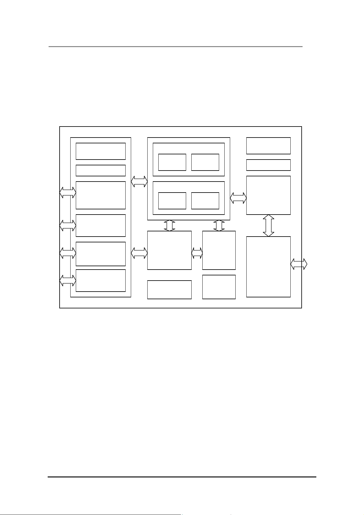
3.1 Block Diagram..............................................................................................6
3.2 Functional Overview.....................................................................................7
4. Pinning Information.........................................................................................9
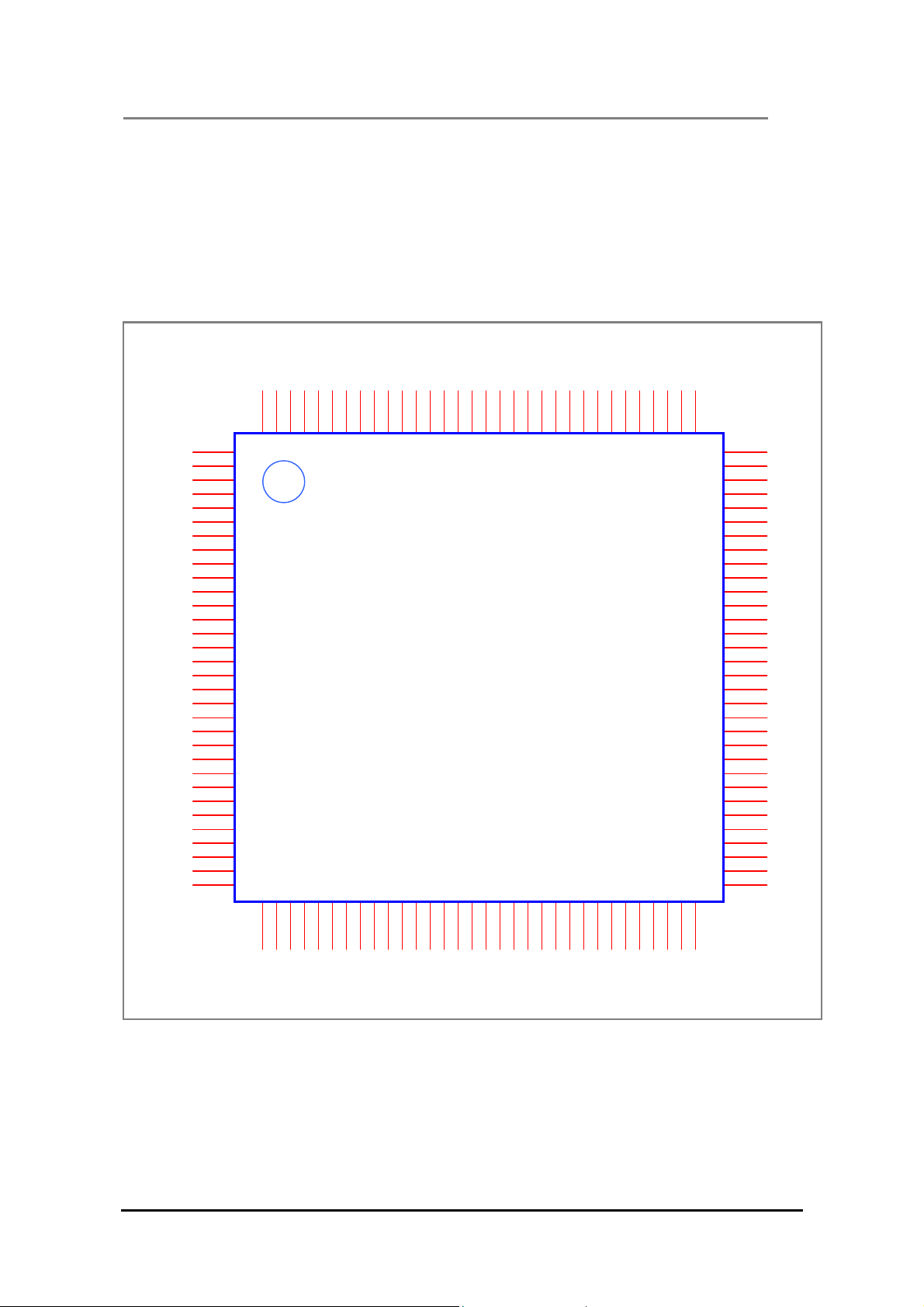
4.1 Pin Assignment.............................................................................................9
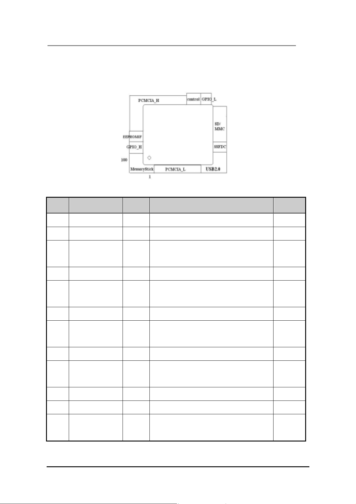
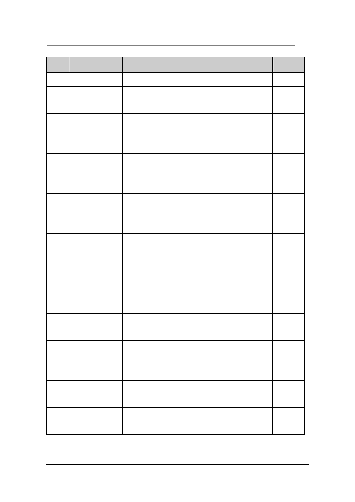
4.2 Pin Description ...........................................................................................10
5. Electrical Characteristics..............................................................................16
5.1 Recommended Operation Conditions.........................................................16
5.2 DC Characteristics......................................................................................16
5.3 AC Electrical Characteristics ......................................................................16
6. Package Information......................................................................................21
7. Revision History.............................................................................................22
©2000-2001 Genesys Logic Inc.—All rights reserved. Page 2
Page 3

GL816 – USB 2.0 Flash Card Reader Controller
1. General Description
The GL816 is a highly integrated, flexible application USB 2.0 Multi-Interface
Flash Card Reader controller. It supports USB 2.0 high-speed transmission to
PCMCIA, CompactFlash
TM
(SD), Multi Media Card
TM
(CF), Micro Drive, SmartMedia
TM
(MMC), and MemoryStick
chip. Besides the flash card interface controller each, the GL816 integrates
Genesys Logic own design USB 2.0 high-speed UTMI (USB 2.0 Transceiver
Macrocell Interface) transceiver. As a single chip solution for USB 2.0 multi flash
card reader, the GL816 complies with Universal Serial Bus specification rev. 2.0,
USB Storage Class specification ver.1.0, and flash card interface specification
each.
TM
(SM), Secure Digital
TM
(MS) interface on one
The GL816 can support different kinds of multi-interface combinations. For the
best performance consideration, the GL816 integrates high efficiency card
interface hardware engine for data transfer, and the 48MHz feature-enhanced
8051 micro-controller. The GL816 also supports firmware upgrade via USB
interface, and external flash read/ write for firmware upgrade and other
applications. With the advanced mobile consideration in the IA application, the
GL816 can support Inter-Media transfer, it means that the data transfer between
different cards doesn’t need the support of USB host in PC system.
The GL816 equips dedicated power control pins for different cards and power /
busy indication. And the pin assignment design fits to card sockets to provide
easier PCB layout. With 8 additional GPIOs, and firmware controllable CD, CE
pins, the GL816 can be programmed to fit your various design in USB 2.0 high
speed multi-interface flash card reader applications.
©2000-2001 Genesys Logic Inc.—All rights reserved. Page 3
Page 4

GL816 – USB 2.0 Flash Card Reader Controller
2. Features
Supports PCMCIA, CompactFlash
(MS), Secure Digital
TM
(SD) and Multi Media Card
TM
(CF), SmartMedia
TM
Complies with 480Mbps Universal Serial Bus specification rev. 2.0.
Complies with USB Storage Class specification rev. 1.0. (Bulk only protocol).
Operating System supported: Win XP/ 2000/ Me/ 98/ 98SE; Mac OS 9.x/ X.
Supports 1 device address and up to 10 endpoints: Control (0)/ Bulk Read (1)/ Bulk
Write (2)/ Interrupt (3), and 3 optional Bulk Read/ Write endpoints pair.
Integrated USB 2.0 Transceiver Macrocell Interface (UTMI) transceiver and Serial
Interface Engine (SIE).
Integrated 8051 micro-controller with enhanced feature:
- Supports 48MHz clock rate.
TM
(SM), MemoryStick
TM
(MMC) interface on one chip.
- 12 clocks per instruction cycle.
- Embedded 24KB Mask ROM and 2KB+256B SRAM.
- Supports external 64KB ROM/ Flash for design flexibility.
Supports firmware upgrade via USB interface.
Supports external flash read/ write for firmware upgrade and other applications.
Supports serial EEPROM 93C86 interface for the flexibility of vendor or firmware
parameters, EEPROM size up to 2KB.
High efficiency card interface hardware engine for data transfer.
Shared pins between PCMCIA and SmartMedia
TM
interface.
PCMCIA interface:
- Supports address up to 16 bits, with fix and incremental mode.
- Supports 8 / 16 bit data mode and different timing.
- Supports WAIT# detection.
- Supports multi signal level (3.3 / 5V).
- Other control signals like CD1#, CD2#, CE1#, CE2# … etc.
SmartMedia
TM
interface:
- Supports address up to 4 bytes, 8 bit data width and different speed.
- Supports different page size, and automatic append redundant area data (8/16
bytes).
- Hardware ECC generation and verification.
- Supports firmware correct page ECC error capability.
- Supports automatic page copy (source page read + destination page write).
©2000-2001 Genesys Logic Inc.—All rights reserved. Page 4
Page 5

GL816 – USB 2.0 Flash Card Reader Controller
MemoryStick
TM
interface
- Complies with MemoryStick interface specification.
- Supports hardware BS/SDIO/SCLK signals.
- Supports INS signal.
- Supports automatic CRC16 generation and verification.
- Supports hardware CMD timeout detection.
- Supports different clock rate up to 24 MHz.
Secure Digital
TM
/ Multi Media CardTM interface
- Complies with Secure Digital / MMC interface specification.
- Supports both SD / MMC mode access: CLK/CMD/DAT0/DAT1/DAT2/DAT3.
- Command transmit and response receive can be enabled separately.
- Automatic CRC7 generation for command and CRC7 verification for response on
CMD.
- Supports automatic CRC16 generation and verification on DAT3-0.
- In addition to full packet transaction, optional single byte/ bit operation on both
CMD and DAT line/ lines.
- Data processing in block or byte.
- Supports different clock rate from 375 KHz to 24 MHz
.
Dedicated power control pins for different cards and power / busy indication.
Build-in power-on reset (POR) and low-voltage detector (LVD).
3.3 Volt operation.
Pin assignment fits to card sockets to provide easier PCB layout.
Supports 8 additional GPIOs and firmware controllable CD, CE pins.
Available in 128-pin LQFP package.
©2000-2001 Genesys Logic Inc.—All rights reserved. Page 5
Page 6
GL816 – USB 2.0 Flash Card Reader Controller
3. Function Block
3.1 Block Diagram
MHE
MHE Control
MCFIFO
PCMCIA
TXFIFO
DA T A A DATA B
RXFIFO
EP0 FIFO
EP3 FIFO
SIE
MIF
MemoryStick
MIF
SD/ MMC
MIF
DA T A A DATA B
USB register
+ FIFO
Control
8051
Core
UTM
SmartMedia
MIF
Mask ROM
SRAM
©2000-2001 Genesys Logic Inc.—All rights reserved. Page 6
Page 7

GL816 – USB 2.0 Flash Card Reader Controller
3.2 Functional Overview
3.2.1 UTM
The USB 2.0 Transceiver Macrocell, it’s the analog circuitry that handles the low
level USB protocol and signaling, and shifts the clock domain of the data from the
USB 2.0 rate to one that is compatible with the general logic.
3.2.2 SIE
The Serial Interface Engine, which contains the USB PID and address recognition
logic, and other sequencing and state machine logic to handle USB packets and
transactions.
3.2.3 EP0 FIFO
It is composed of TX0FIFO and RX0FIFO, with 64-byte FIFO each, and it is used for
endpoint 0 data transfer.
3.2.4 EP3 FIFO
It’s an 8-byte FIFO for endpoint 3.
3.2.5 Bulk FIFO
It is composed of TXFIFO and RXFIFO for data transmission and receiving
respectively, also with different modes support:
3.2.5.1 TXFIFO:
1. To ensure the continuous data transmission, TXFIFO includes 512 bytes
DATA-A FIFO, 512 bytes DATA-B FIFO, and two 16 bytes corresponding
redundant areas. All can be directly accessed by 8051 µC.
2. Normally SIE popes data, MHE pushes data for DATA A/B FIFOs, and
redundant area is pushed by MHE when SmartMedia MIF is enabled and
popped by uC.
3. Supports uC single byte access for SmartMedia ECC error correction.
4. At transmit mode SIE won’t transmit data filled in TXFIFO before uC complete
the data integrity checking.
3.2.5.2 RXFIFO:
1. To ensure the continuous data transmission, RXFIFO includes 512 bytes
DATA-A FIFO, 512 bytes DATA-B FIFO, and 16 bytes single redundant area. All
can be directly accessed by 8051 µC.
©2000-2001 Genesys Logic Inc.—All rights reserved. Page 7
Page 8

GL816 – USB 2.0 Flash Card Reader Controller
2. Normally MHE popes data, SIE pushes data for DATA A/B FIFOs, and
redundant area is pushed by uC and popped by MHE when SmartMedia MIF is
enabled.
3.2.5.3 Buffer Mode:
1. Buffer mode is enabled by firmware and is used to copy data block from source
to destination in same card for SmartMedia or MemoryStick applications.
2. Under Buffer mode, firmware can enable MIF to read source data block to
TXFIFO, check the data integrity, then enable MIF to write data in TXFIFO to
destination data block space on memory card.
3. For SmartMedia application, the redundant data write to destination data block
space is from redundant area of RXFIFO.
3.2.6 MHE (Media Hardware Engine)
The Media Hardware Engine contains 4 MIF (Media Interface), MHE control and
MCFIFO.
3.2.6.1 MIF (Media Interface):
There are PCMCIA MIF, SmartMedia MIF, MemoryStick MIF, and Secure Digital/
Multi Media Card MIF in MHE.
3.2.6.2 MCFIFO (Media Control FIFO):
It’s a 64-byte FIFO that shared by MemoryStick and SD/ MMC MIF. In MemoryStick
application, the MCFIFO is used for register read and write function; In SD/ MMC
application, it is used for command and response.
3.2.6.3 SMAFIFO (SmartMedia
TM
Address FIFO)
It’s a 4-byte FIFO for SmartMedia address only.
©2000-2001 Genesys Logic Inc.—All rights reserved. Page 8
Page 9
K
A
A
A
A3 A
A
A
A8 A
A
A
64
GL816 – USB 2.0 Flash Card Reader Controller
4. Pinning Information
4.1 Pin Assignment
INS
SCLK
PCCD1#
D11
D12
PGND1
D13
D14
PCCE1#
D15
A10
PCCE2#
OE#
PCVS1#
PVIO1
A11
IOR#/ RE#
IOW#/ WR#
RPU
AVDD1
VPF
VPH
VMF
VMH
AGND1
RREF
SDIO
BS
NVMD7
NVMD6
NVMD5
NVMD4
DVDD3
GPIO7
NVMD3
NVMD2
NVMD1
NVMD0
DO
DI
SK
CS
NVMWE#
NVMOE#
1
128
127
126
125
124
AGND2
123
RB#
SMCE#
SMWPD#
2
D3
3
4
D4
5
6
D5
7
8
D6
9
10
11
D7
12
13
14
15
16
17
18
19
20
21
22
A9
23
24
25
26
27
28
29
30
31
32
33343536373839404142434445464748495051525354555657585960616263
XI
XO
AVDD2
122
SMCD#
121
119
118
117
116
120
115
GL816
128 LQFP
NVMA15
NVMA11
NVMA14
NVMA13
NVMA12
NVMA10
DAT2
111
114
113
112
CL
CMD
DAT3
13 A14
DGND3
DGND2
110
109
108
107
DAT1
DAT0
NVMA9
NVMA8
16 A15 A12 A7
WE#
IREQ#
106
105
104
103
102
101
NVMA^
NVMA7
NVMA5
NVMA4
NVMA3
NVMA2
CD#
GPIO6
100
PWR33C
6
GPIO5
999897
DVDD1
DVDD2
96
95
94
93
92
91
90
89
88
87
86
85
84
83
82
81
80
79
78
77
76
75
74
73
72
71
70
69
68
67
66
65
PCVS2#
5
PCRST
4
WAIT#
2/ SMWP#
REG#
PVIO2
1/ ALE
0/ CLE
D0
D8
D1
D9
D2
D10
PCCD2#
PGND2
DGND1
BSYIND
PWRIND
EXTRST#
PWR33CB
GPIO4
GPIO3
NVMCS#
NVMA0
NVMA1
GPIO2
GPIO1
WPD#
©2000-2001 Genesys Logic Inc.—All rights reserved. Page 9
Page 10
GL816 – USB 2.0 Flash Card Reader Controller
4.2 Pin Description
GL816
Pin# Name I/O Description Note
1 INS B/I MemoryStick INS pu
2 SCLK O MemoryStick SCLK
PCMCIA data 3 /
3 D3 B
SmartMedia data 3
4 PCCD1# B/I PCMCIA CD1# pu
PCMCIA data 4 /
5 D4 B
SmartMedia data 4
6 D11 B PCMCIA data 11
PCMCIA data 5 /
7 D5 B
SmartMedia data 5
8 D12 B PCMCIA data 12
PCMCIA data 6 /
9 D6 B
SmartMedia data 6
10 PGND1 P Pad GND #1
11 D13 B PCMCIA data 13
PCMCIA data 7 /
12 D7 B
SmartMedia data 7
©2000-2001 Genesys Logic Inc.—All rights reserved. Page 10
Page 11
GL816 – USB 2.0 Flash Card Reader Controller
Pin# Name I/O Description Note
13 D14 B PCMCIA data 14
14 PCCE1# B/O PCMCIA CE1# pu
15 D15 B PCMCIA data 15
16 A10 O PCMCIA address 10
17 PCCE2# B/O PCMCIA CE2# pu
18 OE# O PCMCIA OE#
PCMCIA VS1#
19 PCVS1# B/I
ATAPI DMARQ
20 PVIO1 P Power (5 / 3.3V) for pin 3-24
21 A11 O PCMCIA address 11
PCMCIA IOR# /
22 IOR# / RE# O
SmartMedia RE#
23 A9 O PCMCIA address 9
PCMCIA IOW# /
24 IOW# / WR# O
SmartMedia WR#
25 RPU A USB resistor pull up
26 AVDD1 P Analog VDD #1
27 VPF B FS D+
28 VPH B HS D+
29 VMF B FS D-
30 VMH B HS D-
31 AGND1 P Analog GND #1
32 RREF A Reference resistor
33 AVDD2 P Analog VDD #2
34 XI I Crystal input
35 XO B Crystal input
36 AGND2 P Analog GND #2
©2000-2001 Genesys Logic Inc.—All rights reserved. Page 11
Page 12
GL816 – USB 2.0 Flash Card Reader Controller
Pin# Name I/O Description Note
37 RB# B/I SmartMedia RDY/BSY# pu
38 SMCE# B/O SmartMedia CE# pu
39 SMWPD# B/I SmartMedia Write Protect Detect pu
40 SMCD# B/I SmartMedia CD# pu
41 NVMA15 O Ext. flash address 15
42 NVMA14 O Ext. flash address 14
43 NVMA13 O Ext. flash address 13
44 NVMA12 O Ext. flash address 12
45 NVMA11 O Ext. flash address 11
46 NVMA10 O Ext. flash address 10
47 DAT2 B/SO SD DAT2 pu
48 DAT3 B/SO SD DAT3 pu
49 CMD B/SO SD/MMC CMD pu
50 CLK O SD/MMC CLK
51 DAT1 B/SO SD DAT1 pu
52 DAT0 B/SO SD/MMC DAT0 pu
53 NVMA9 O Ext. flash address 9
54 NVMA8 O Ext. flash address 8
55 NVMA7 O Ext. flash address 7
56 NVMA6 O Ext. flash address 6
57 NVMA5 O Ext. flash address 5
58 NVMA4 O Ext. flash address 4
59 NVMA3 O Ext. flash address 3
60 NVMA2 O Ext. flash address 2
61 CD# B/I SD/MMC CD# pu
62 PWR33CA O PCMCIA 3.3V power control pd
63 DVDD1 P Digital VDD #1
©2000-2001 Genesys Logic Inc.—All rights reserved. Page 12
Page 13
GL816 – USB 2.0 Flash Card Reader Controller
Pin# Name I/O Description Note
64 DVDD2 P Digital VDD #2
65 WPD# B/I SD/MMC Write Protect Detect pu
66 GPIO1 B GPIO1 odpu
67 GPIO2 B GPIO2 odpu
68 NVMA1 O Ext. flash address 1
69 NVMA0 O Ext. flash address 0
70 NVMCS# O Ext. flash CS# pu
71 GPIO3 B GPIO3 odpu
72 GPIO4 B GPIO4 odpu
73 PWR33CB O Card 3.3V power control pd
74 EXTRST# I External reset pu
75 PWRIND O Power indicator pd
76 BSYIND O Busy indicator pd
77 DGND1 P Digital GND #1 pu
78 PGND2 P Pad GND #2
79 PCCD2# B/I PCMCIA CD2#
80 D10 B PCMCIA data 10
PCMCIA data 2 /
81 D2 B
SmartMedia data 2
82 D9 B PCMCIA data 9
PCMCIA data 1 /
83 D1 B
SmartMedia data 1
84 D8 B PCMCIA data 8
PCMCIA data 0 /
85 D0 B
SmartMedia data 0
PCMCIA address 0 /
86 A0 / CLE O
SmartMedia CLE
©2000-2001 Genesys Logic Inc.—All rights reserved. Page 13
Page 14
GL816 – USB 2.0 Flash Card Reader Controller
Pin# Name I/O Description Note
PCMCIA address 1 /
87 A1 / ALE O
SmartMedia ALE
88 PVIO2 P Power (3.3 / 5V) for pin 79-108
89 REG# B/O PCMCIA REG# pu
PCMCIA address 2 /
90 A2 / SMWP# O
SmartMedia WP#
91 A3 O PCMCIA address 3
92 WAIT# I/SO PCMCIA WAIT# pu
93 A4 O PCMCIA address 4
94 PCRST B PCMCIA RESET pd
95 A5 O PCMCIA address 5
96 PCVS2# B/I PCMCIA VS2# pu
97 A6 O PCMCIA address 6
98 GPIO5 B GPIO5 odpu
99 GPIO6 B GPIO6 odpu
100 A7 O PCMCIA address 7
PCMCIA address 12 /
101 A12 O
ATAPI DMACK#
102 A15 O PCMCIA address 15
103 A16 O PCMCIA address 16
104 IREQ# B/I PCMCIA IREQ# pu
105 WE# O PCMCIA WE#
106 A14 O PCMCIA address 14 / MCS0#
107 A13 O PCMCIA address 13 / MCS1#
108 A8 O PCMCIA address 8
109 DGND2 P Digital GND #2
110 DGND3 P Digital GND #3
©2000-2001 Genesys Logic Inc.—All rights reserved. Page 14
Page 15
GL816 – USB 2.0 Flash Card Reader Controller
Pin# Name I/O Description Note
111 NVMOE# O Ext. flash OE#
112 NVMWE# O Ext. flash WE#
113 CS O 93C86 CS
114 SK O 93C86 Clock
115 DI O 93C86 Data in
116 DO I/SO 93C86 Data out pd
117 NVMD0 B Ext. flash Data 0 pd
118 NVMD1 B Ext. flash Data 1 pd
119 NVMD2 B Ext. flash Data 2 pd
120 NVMD3 B Ext. flash Data 3 pd
121 GPIO7 B GPIO7 odpu
122 DVDD3 P Digital VDD #3
123 NVMD4 B Ext. flash Data 4 pd
124 NVMD5 B Ext. flash Data 5 pd
125 NVMD6 B Ext. flash Data 6 pd
126 NVMD7 B Ext. flash Data 7 pd
127 BS O MemoryStick BS
128 SDIO B MemoryStick SDIO pd
Notation:
Description
Note
O Output
I Input
B Bi-directional
B/I Bi-directional, default input
B/O Bi-directional, default output
P Power
A Analog
SO Automatic output low when suspend
pu Internal pull up
pd Internal pull down
odpu Open drain with internal pull up
©2000-2001 Genesys Logic Inc.—All rights reserved. Page 15
Page 16
GL816 – USB 2.0 Flash Card Reader Controller
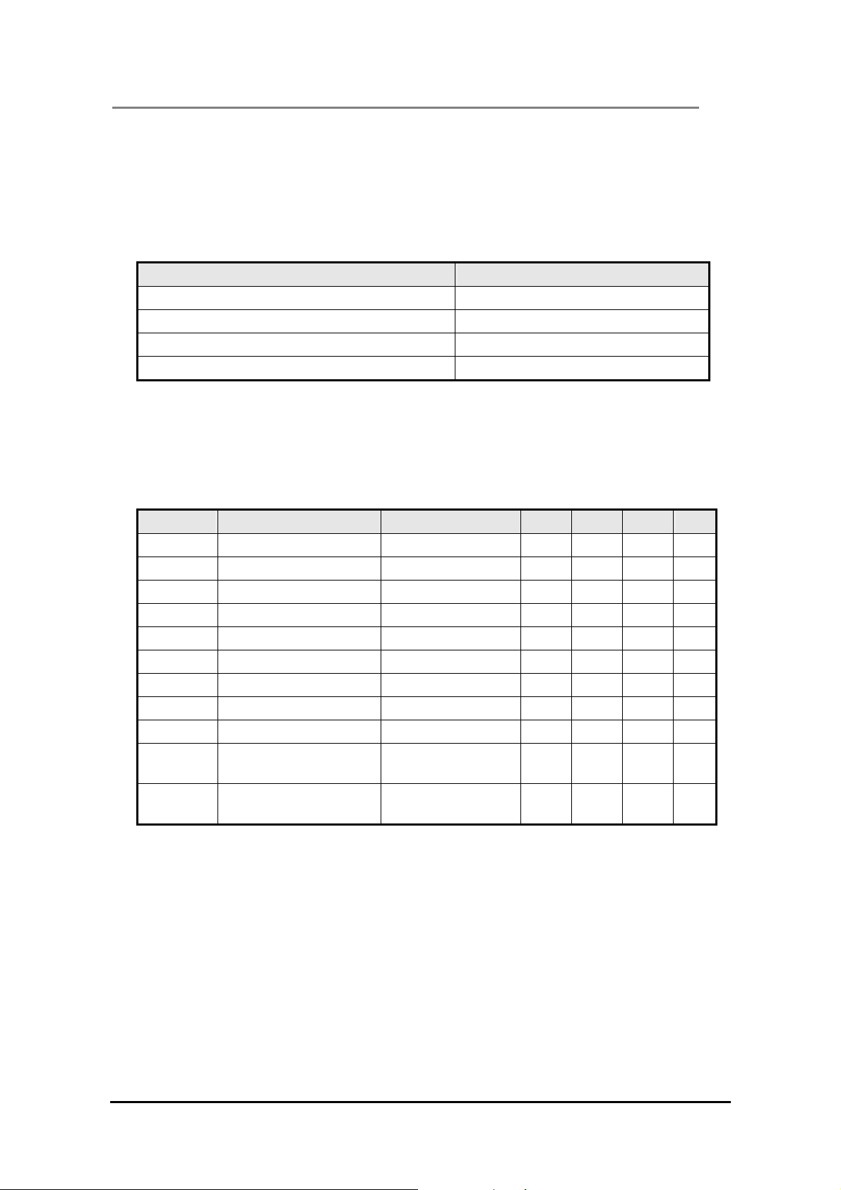
5. Electrical Characteristics
5.1 Recommended Operation Conditions
Item Value
TA (Ambient Temperature under bias) 0°C to 70°C
Supply Voltage +3.0V to +3.6V
Ground Voltage 0V
F
12 MHz ± 100ppm
OSC
5.2 DC Characteristics
Parameter Description Condition Min. Typ. Max. Unit
VCC Supply Voltage 3.0 3.6 V
VIH Input High Voltage 2.6 5 V
VIL Input Low Voltage 0.0 0.7 V
II Input Leakage current 0 < VIN < VCC µA
VOH Output High Voltage 3.0 V
VOL Output Low Voltage 0.2 V
IOH Output Current High mA
IOL Output Current Low mA
CIN Input Pin Capacitance 2.0 pF
I
Suspend current
SUSP
ICC Supply current
1.5K external
pull-up included
Connect to USB
with 8051 operating
µA
mA
5.3 AC Electrical Characteristics
5.3.1 UTMI Transceiver
The GL816 is fully compatible with Universal Serial Bus specification rev. 2.0 and
USB 2.0 Transceiver Macercell Interface (UTMI) specification rev. 1.01. Please
refer to the specifications for more information.
©2000-2001 Genesys Logic Inc.—All rights reserved. Page 16
Page 17
GL816 – USB 2.0 Flash Card Reader Controller
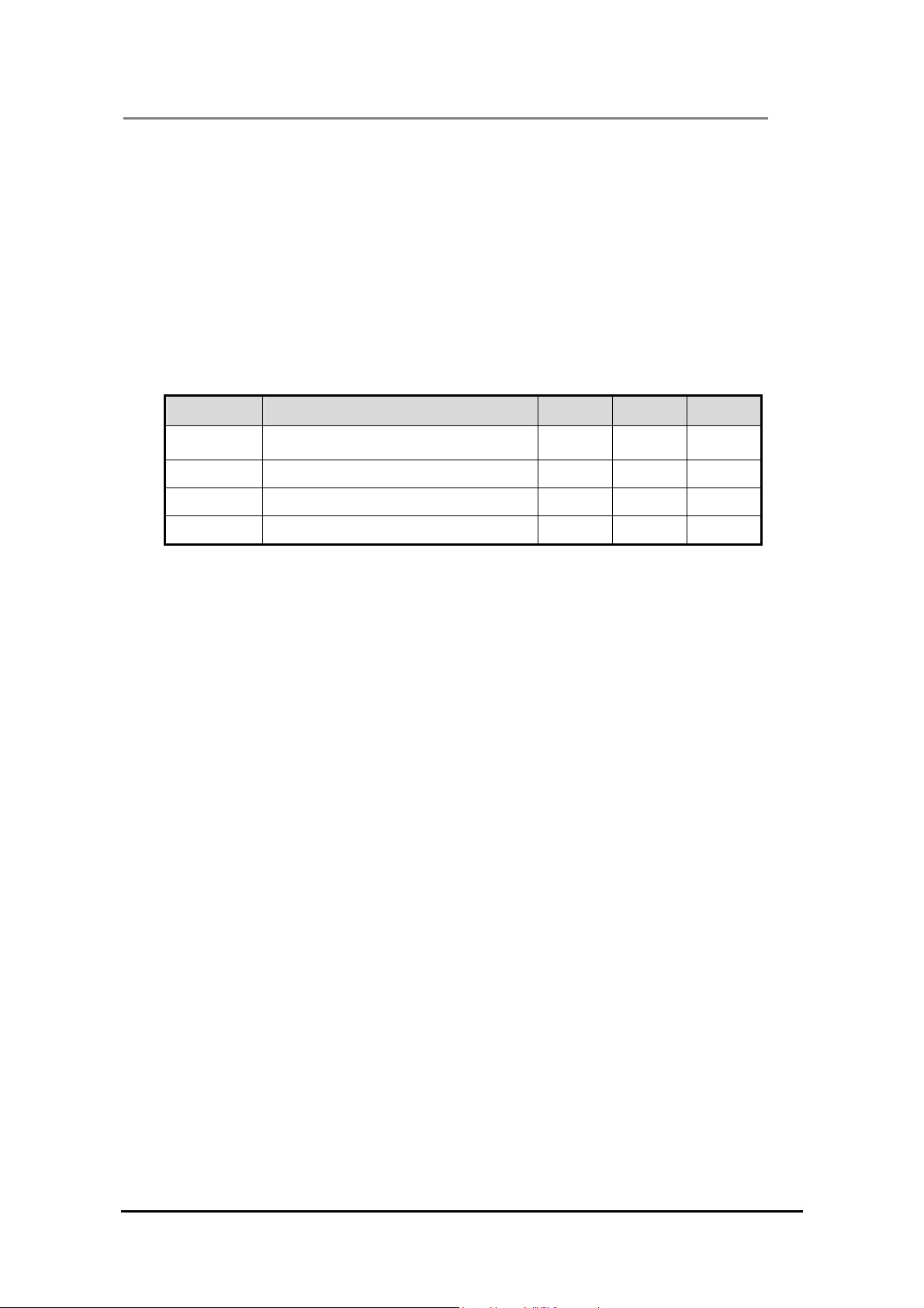
5.3.2 External Flash
NVMA[0..15]
\\\\\;\\\\\\\\\\\\\\@’\\\\\
dddddxdddddddddddddddxddddd
Twc
NVMOE# lllllrhhhhhhhhhhhhhhhflllll
\\\\\;\\\@;\\\\\@’\\\;\\@’\
Tow Tww Tra
NVMWE# hhhhhhhhhhfllllllrhhhhhhhhh
NVMD[0..7] dddddxddddxddddddddddxdddxd
Parameter Description Min Typ Max
TWC Write data cycle time 102.5
TWW Write pulse width 41.6
TOW OE# to WE# time 38.6
T
RA
5.3.3 PCMCIA
Read
Read Access time
90
Unit: ns
A[0..16] dxddddddddddddddddddddddddd
\\\\\\\\\\\\\;\\\@;\\@’\\\\
Tds Tdh
OE# / IOR# hhhhhhhfllllllllllrhhhhhhfl
\\\\\\\;\\\\\\\\\\\\\\\\@’\
Tdc
D[0..15] zzzzzzzzzzzzznddddddddozzzz
Write
A[0..16]
\\\\;\\@;\\\\\\\\@;\\@’\\\\
dxddddddddddddddddddddddddd
Tdp Tdd
Tpw
WE# / IOW# hhhhhhhhflllllllllrhhhhhhfl
\\\\\\\;\\\\\\\\\\\\\\\\@’\
Tdc
D[0..15] zzzzndddddddddddddddddozzzz
©2000-2001 Genesys Logic Inc.—All rights reserved. Page 17
Page 18
GL816 – USB 2.0 Flash Card Reader Controller
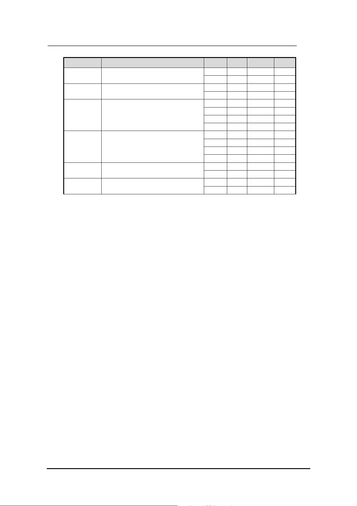
Parameter Description Mode Min Typ Max
Tds Data setup time (read)
Tdh Data hold time (read)
Tdc Access cycle time (read / write)
Tpw Control pulse width (read / write)
Tdp Data pre-output time (write)
Tdd Data delay time (write)
0, 1 88.3
2, 3 38.3
0, 1 2
2, 3 2
0 666.4
1 416.5
2 222.1
3 166.5
0 333.2
1 166.6
2 133.2
3 66.6
0, 1 26.6
2, 3 1.6
0, 1 41.6
2, 3 16.6
Unit: ns
5.3.4 SmartMedia
Read
\\\\\;\\\\\\\\\\\\\@;\\\\\@’
Tcr
Trw
RE# hhhhhfllllllrhhhhhhhfllllllr
\\\\\\\\;\\@;\@’\\\\\\\\\\\\
Tds Tdh
D[0..7] zzzzzzzznddddddozzzzzzzznddd
Write
CLE
\;\\\@’\\\\\\\\\\\\\;\\\\@’\
lrhhhhflllllllllllllllllllll
Tcw
Twc
ALE lllllllllrhhhhhhhfllllllllll
Tww
\\\\\\\\\\\\\\\\\\\\;\@’\\\\
WE# hhhhhhhhhhhhhhhhhhhhfllrhhfl
Tcd Tai
Tad
Tdw Tdw
Tdp
Tdd
\;@;@’\\\;@’;@;@’\\\\;@;@’\\
D[0..7] zzzndozzzzndozndozzzzndddozn
©2000-2001 Genesys Logic Inc.—All rights reserved. Page 18
Page 19
GL816 – USB 2.0 Flash Card Reader Controller
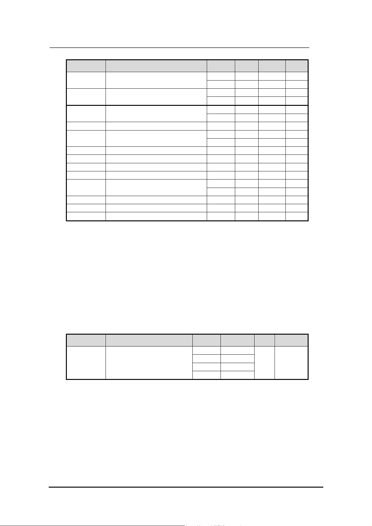
Parameter Description Mode Min Typ Max
Tcw CLE active width
Twc Write data cycle time
Tww Write pulse width
Tcd CLE-to-command delay 33.3
Tdw Data width
Tad ALE-to-address delay 33.3
Tai Address data interval time 33.3
Tdp Data pre-output delay 33.3
Tdd Data delay time 33.3
Tcr Read data cycle time
Trw Read pulse width 100
Tds Data setup time 40
Tdh Data hold time 2
Normal 165
Slow 198
Normal 100
Slow 166
Normal 66
Slow 100
Normal 67
Slow 100
Normal 133.3
Slow 166.6
Unit: ns
5.3.5 MemoryStick
BS llrhhhhhhhhhhhhhhhfllllllllll
SCLK lllrfrfrfrfrfrfrfrfrfrfrfrfrf
SDIO ddddxdddddddddddddddxdddddddd
Parameter Description Mode Typ Unit Remark
0 1.5M
Fck SCLK frequency
1 6M
2 15M
3 24M
Hz
5.3.6 Secure Digital / MultiMedia Card
CMD dddxdxdxdddddddddddddddddxdddd
CLK rfrfrfrfrfrfrfrfrfrfrfrfrfrfrf
DAT dddddddddddddxdddddddddddxdddd
©2000-2001 Genesys Logic Inc.—All rights reserved. Page 19
Page 20
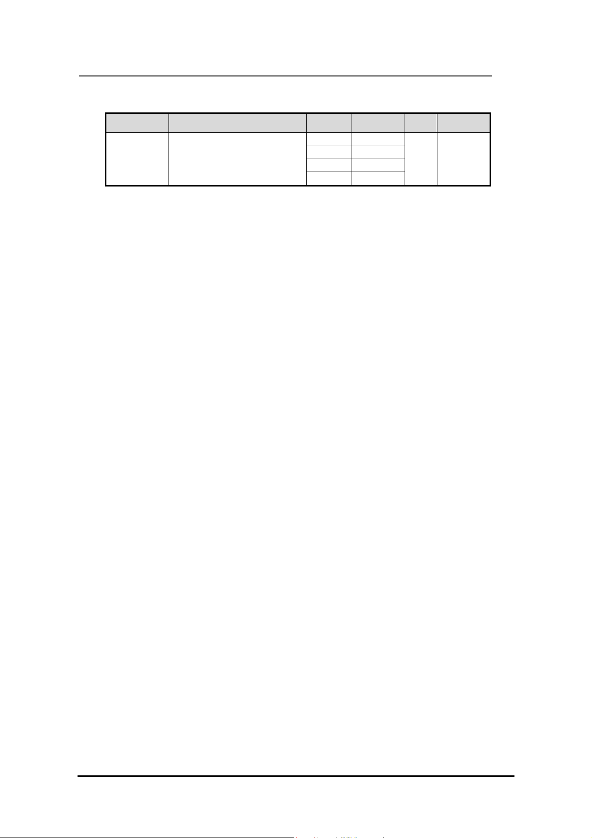
GL816 – USB 2.0 Flash Card Reader Controller
Parameter Description Mode Typ Unit Remark
Fck CLK frequency
0 375K
1 6M
2 15M
Hz
3 24M
©2000-2001 Genesys Logic Inc.—All rights reserved. Page 20
Page 21
GL816 – USB 2.0 Flash Card Reader Controller
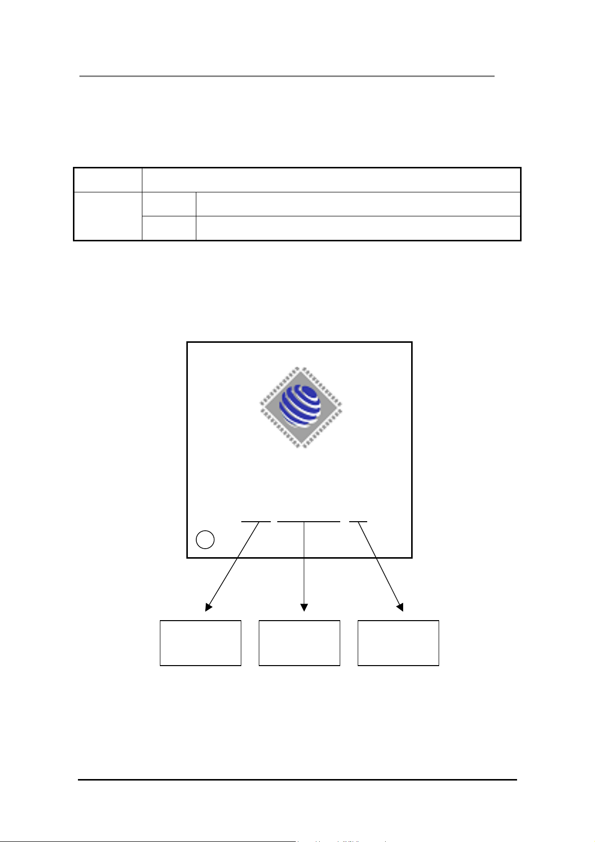
6. Package Information
Type No. Package
Name Description
GL816
LQFP128 Plastic low profile quad flat package; 128 leads; Body 14 x14 x1.4 mm
EX:
Date Code:
GL816
0212MC51101-01
Foundry
Code
YYWW
©2000-2001 Genesys Logic Inc.—All rights reserved. Page 21
Lot No.
Number
Page 22
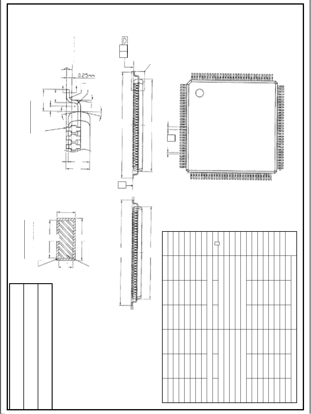
GAGE PLANE
DETAIL “X”
(20/1)
SECTION A-A
L1
SEATING
PLANE
WITH PLATING
1
SY
θ
A
A
R1
R2
L
S
θ3
θ1
θ2
D
“X”
D1
128
1
97
LQFP128
GL816
e
A1
A
A2
b
32
33
64
6596
S
c c1
BASE METAL
b
b
e
E
E1
SYMBOL
LQFP128 (14x14x1.4 mm)
GL816
Genesys Logic, Inc.
0°0°θ1
80.20s
13°12°11°13°12°11°θ3
13°12°11°13°12°11°θ2
30.08R1
DIMENSION (MIL)DIMENSION (MM)
551 BSC14.00 BSCE1
630 BSC16.00 BSCE
551 BSC14.00 BSCD1
16 BSC0.40 BSC
39 REF1.00 REFL1
7°3.5°0°7°3.5°0°θ
30.075Y
3024180.750.600.45L
830.200.08R2
630 BSC16.00 BSCD
7.56.350.190.160.13b1
640.160.09c1
840.200.09c
9750.230.180.13b
MAX.NOM.MIN.MAX.NOM.MIN.
5755531.451.401.35A2
631.60A
620.150.05A1
Page 23

GL816 – USB 2.0 Flash Card Reader Controller
7. Revision History
Version Description Date
1.0 First draft 2002/05/10
1.1 Change the package from QFP128 to LQFP128 2002/07/17
1.2 Add package information data 2002/09/20
©2000-2001 Genesys Logic Inc.—All rights reserved. Page 22
 Loading...