

Page 1

GL841 USB 2.0 2-in-1 Scanner Controller
7 Version 1.6
Genesys Logic, Inc.
GL841
High Speed USB 2.0
Two-in-one Scanner Controller
SPECIFICATION Ver. 1.6
June 11, 2002
Genesys Logic, Inc.
10F, No.11, Ln. 155, Sec. 3, Peishen Rd., Shenkeng, Taipei, Taiwan
Tel: 886-2-2664-6655 Fax: 886-2-2664-5757
http://www.genesyslogic.com
Page 2

GL841 USB 2.0 2-in-1 Scanner Controller
Version 1.6
2
INDEX
1
General Description.............................................................................................................................. 3
2 Feature................................................................................................................................................... 3
3 System Block Diagram......................................................................................................................... 5
4 Function Block Diagram......................................................................................................................6
5 Hardware description........................................................................................................................... 7
6 Application Description ..................................................................................................................... 14
7 Command set descriptions................................................................................................................. 23
8 Package…………………………………………….………………………………………………….48
Page 3

GL841 USB 2.0 2-in-1 Scanner Controller
Version 1.6
3
1 GENERAL DESCRIPTION
Genesys Logic's single-chip GL841 (GeneScan™ series) is a high speed, high
performance, low cost and rich scalability controller for scanner. It successfully
integrates scanner function ASIC and USB 2.0 interface controller into one
single-chip. With its high performance design architecture, GL841 is not only
ready for supporting CIS or CCD image sensors (600dpi,1200dpi or 2400dpi
resolution) that are used in flatbed or transparency scanners, but is able to cowork with uni-polar or bi-polar stepping motors. Advanced features of GL841
include five motor acceleration/ deceleration curve tables for high speed motor
moving.
2 FEATURES
! Highly integrated scanner controller chip. (2-in-1; Scanner Controller and USB
2.0 Interface)
! USB 2.0 High Speed (480Mbit) compliance. (USB 2.0 High Speed logo certified)
! Design for sheetfed, flatbed and transparency scanner.
! 12 Mhz Low frequency clock input required for better EMI.
! Flexible 3.3V/5V power selection for pad I/O.
! Adjustable working speed for different usage.
! Fast operation speed. (0.3us/pixel, in 40MHz working clock)
! It costs only 12 seconds for 600dpi A4 size color scanning
! Available sensor types: 600, 1200 and 2400dpi color CIS or CCD.
! Support linear or stagger CCD , such as NEC , Toshiba or Sony CCD
! Support 48-Bits color (16-Bits gray level ) scanning.
! Support color, fine Gray, fast gray and fast B/W scan for CCD.
! Support color,, gray, true gray and B/W scan for CIS.
! Support three scanning types :pixel by pixel(pixel rate), line by line(line rate) and
RGB line by turns(line rate).
! 16 bits white/dark shading and 16-to-8 bits Gamma correction.
! Support digital average and hardware deletion pixel function for speeding up low
resolution scan.
Page 4

GL841 USB 2.0 2-in-1 Scanner Controller
Version 1.6
4
! Support hardware deletion type for DPI function (2400 to 1 DPI ,1 DPI
decrement) .
! Programmable threshold level for B/W.
! Exposure time is adjustable (1 pixel time increment step).
! Scan width (scan area) control for horizontal line( 1 pixel increment step).
! Support 256K*16, 256K*16*2 and 1M*16 bits EDO-DRAM.
! Support 5 acceleration/deceleration motor tables for detailed controllable high
speed motor moving.
! Support controllableg bipolar motor in full, half and quarter steps moving.
! Support controllable uni-polar motor in full and half steps moving.
! Build-in PWM control phase for uni-polar motor.
! Programmable dummy lines to resolve start/stop (discontinuous) problem.
! Watch dog protect for lamp, motor and ASIC.
! Lamp timeout (sleeping) control.
! Support 16 GPIO pins and 2 GPO pins.
! Output motor trigger signal under scanning for ADF.
! 2 Output ports for lamp(include flatbed and transparency with PWM) control.
! Input port for home sensor.
! Power on check status.
! Support LED Blinking.
! Support Back Scanning.
Page 5
GL841 USB 2.0 2-in-1 Scanner Controller
Version 1.6
5
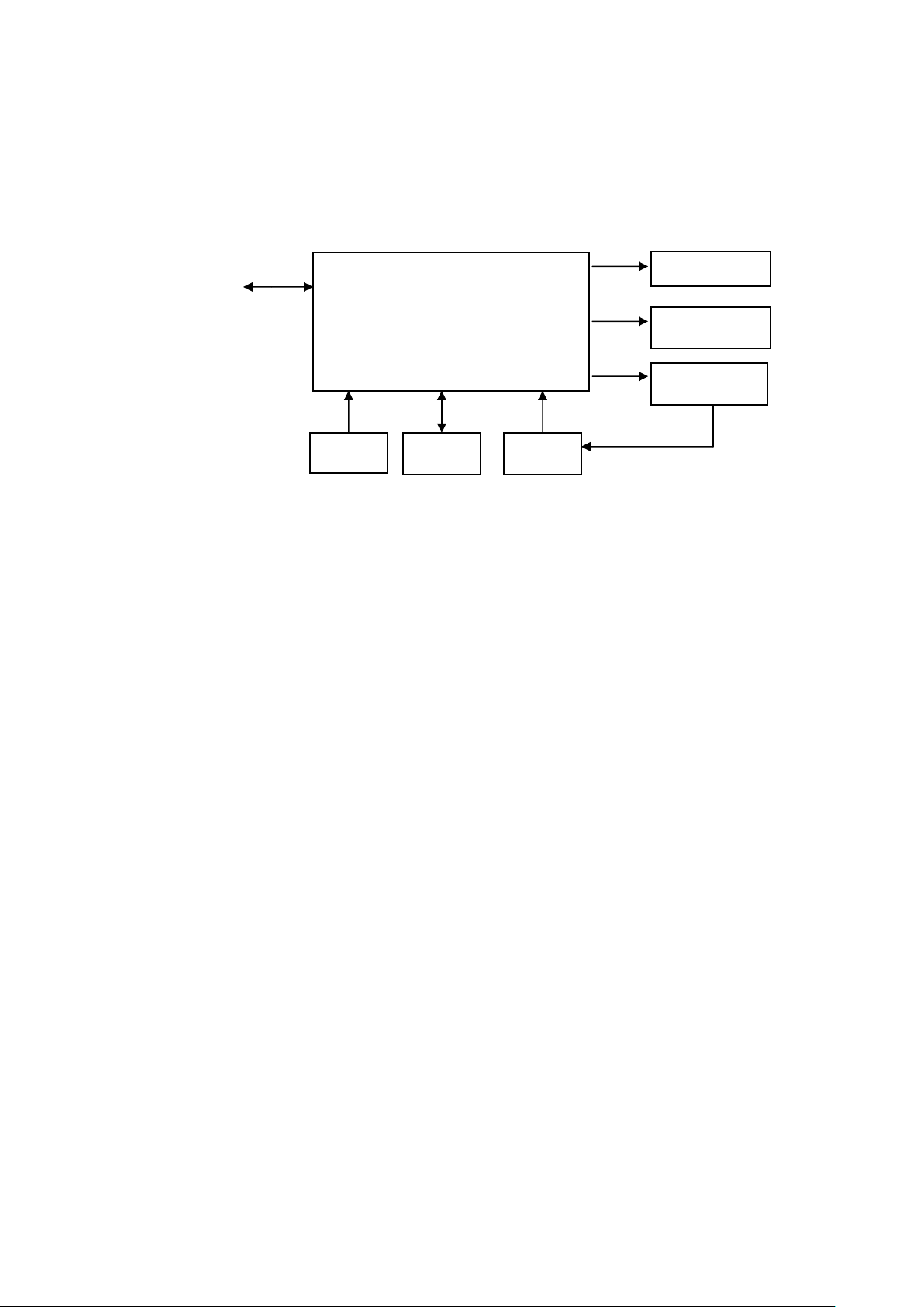
3 SYSTEM BLOCK DIAGRAM
A. USB 2.0 System Block Diagram
Host
12 MHz
GL841
(USB2.0 Interface + Scanner ASIC
Controller)
Two-In-One Controller
DRAM
CCD/CIS
Motor Driver
IO Device
AFE
Page 6
GL841 USB 2.0 2-in-1 Scanner Controller
Version 1.6
6
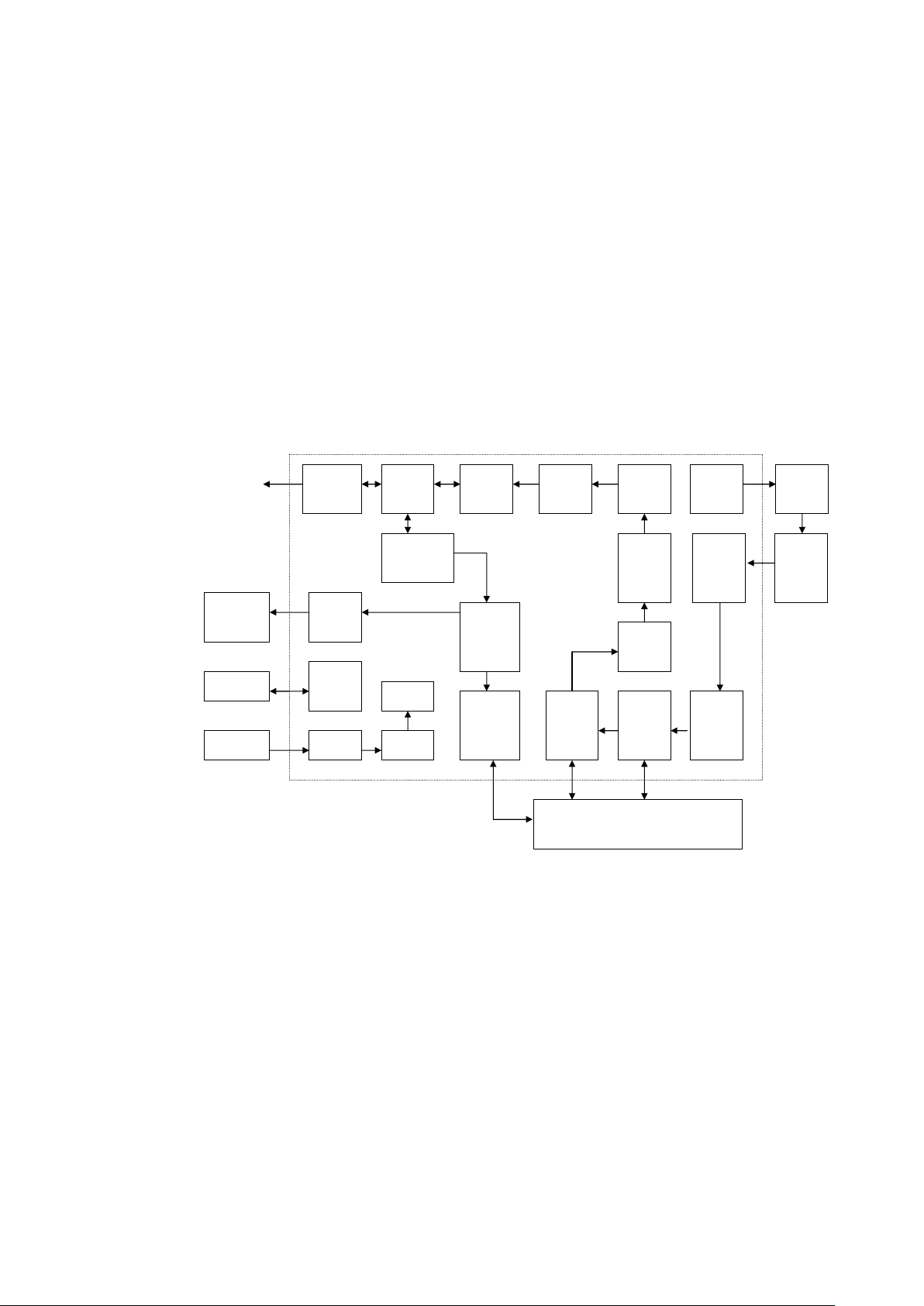
4 FUNCTION BLOCK DIAGRAM
HOST
Motor
control
A/D data
latch
Motor
Driver
12MHz
I/O
CCD/
CIS
CCD/CIS
control
Front-
End(16
Bits)
Dark
Shading
process
White
Shading
process
Shading ,Image and Motor Table DRAM
(256K*16*1) , (256K*16*2) or (1M*16)
Data
Packing
Average
Control
Gamma
Correcion
Black &
White
DPI
control
PLL
watchdog
GPIO
control
EPP
Circuit
Register Write
& Status read
Motor
Moving
Table
Data
Interface
Clk-gen
USB 2.0
Controller
Scanner
Flow
Control
Page 7
GL841 USB 2.0 2-i n -1 Scanner Contr ol ler
7 Version 1.6
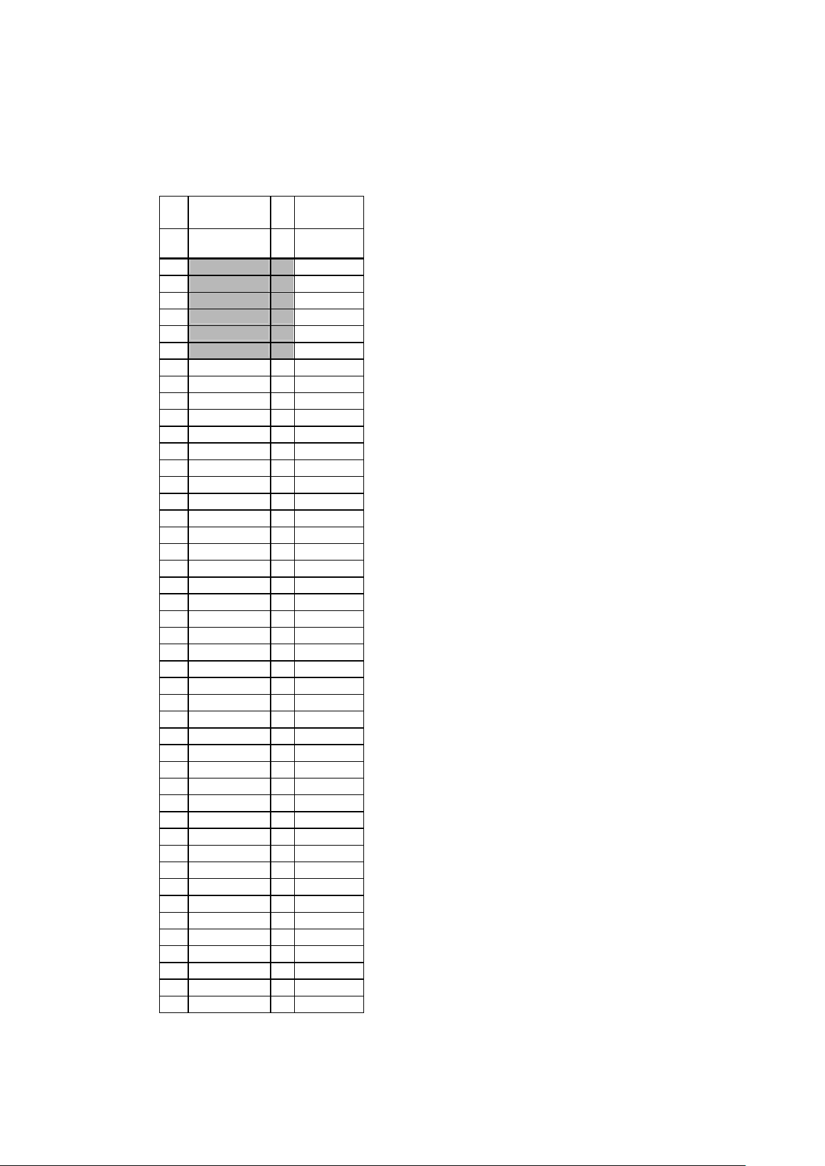
5 HARDWARE DESCRIPTION
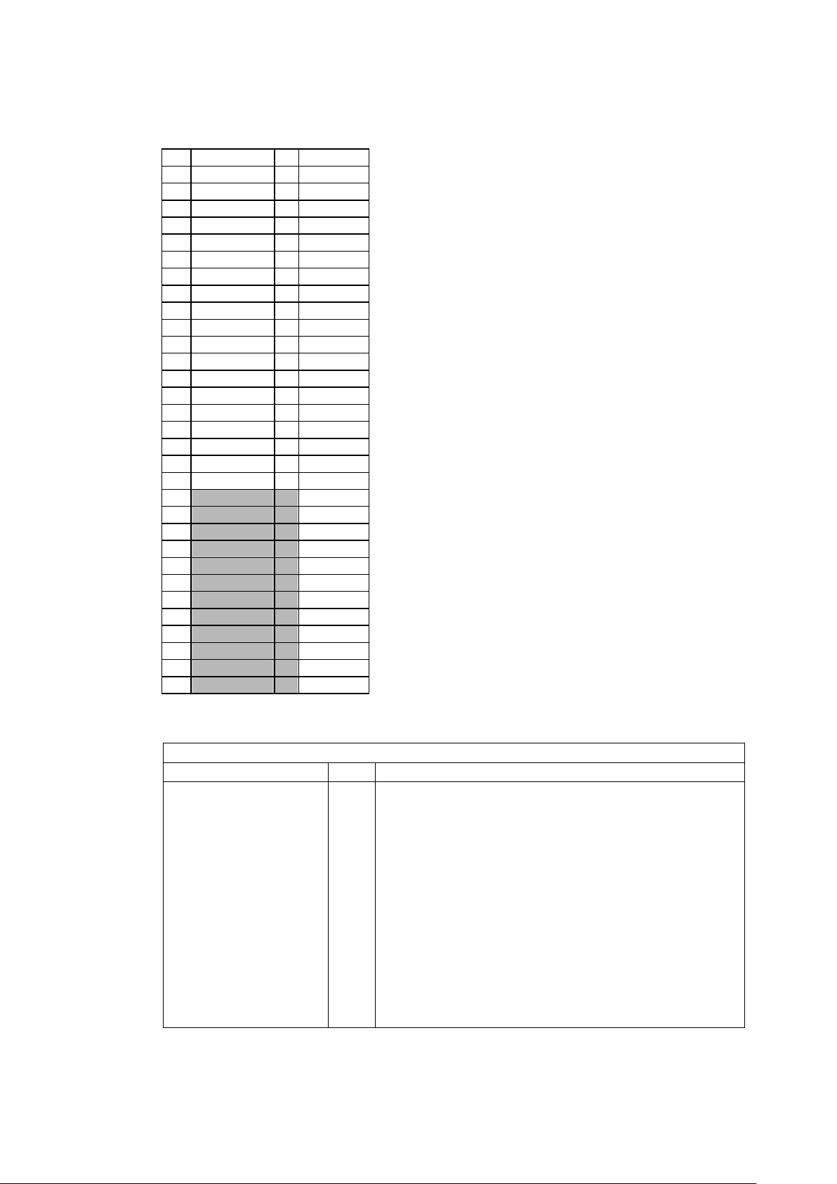
5.1 Pins Assignment & Mode Definition:
SC+USB2.0
ASIC I/O
Cell
TSTSEL[1:0]=0
1
AVCC1 P
2 X2
I/O
3 X1
I
4
AGND1 P
5
DVCC1 P
6
DGND1 P
7 GPIO1
I/O
hbd16rsc
8 GPIO2 I/O hbd16rsc
9 GPIO3 I/O hbd16rsc
10 GPIO4 I/O hbd16rsc
11 GPIO5 I/O hbd16rsc
12 GPIO6 I/O hbd16rsc
13 GPIO7 I/O hbd16rsc
14 GPIO8 I/O hbd16rsc
15 GPIO9 I/O hbd16rsc
16 GPIO10 I/O hbd16rsc
17 GPIO11 I/O hbd16rsc
18 GPIO12 I/O hbd16rsc
19
GPIO13
I/O hbd16rsc
20
GPIO14 I/O
hbd16rsc
21
VccCore1 P
22
GndCore1 P
23
GPIO15 I/O
hbd16rsc
24
GPIO16 I
hbd16rsc
25
Vccio1 P
26
Gndio1 P
27 MTR_SEL0
I
hbd16rsc
28 MTR_SEL1
I
hbd16rsc
29
LAMP_SW O
hbd16rsc
30
XPA_SW O
hbd16rsc
31
LED_B O
hbd16rsc
32 MT_PH0 O hbd16dhk
33 MT_PH1 O hbd16dhk
34 MT_PH2
O
hbd16dhk
35 MT_PH3 O hbd16dhk
36 MT_PH4 O hbd16dhk
37 MT_PH5
I/O
hbd16rsc
38 MT_PH6 O hbd16rsc
39 MT_PH7 O hbd16rsc
40
OP0 I
hbd16dhk
41
OP1 I
hbd16dhk
42
OP2 I
hbd16dhk
43
OP3
I hbd16dhk
44
OP4
I hbd16dhk
45
OP5
I hbd16dhk
Page 8
GL841 USB 2.0 2-i n -1 Scanner Contr ol ler
Version 1.6
8
46
OP6 I
hbd16dhk
47
OP7 I
hbd16dhk
48
Vccio2 P
49
Gndio2 P
50
SDO I
hbd16dhk
51
SDI O
hbd16dhk
52
VccCore2 P
53
GndCore2 P
54
SCLK O
hbd16rsc
55
SEN O
hbd16dhk
56
BSMP O
hbd16rsc
57 VSMP O hbd16rsc
58 MCLK O hbd16rsc
59 CCD_TGX O hbd16rsc
60 CCD_CK1X O hbd16rsc
61 CCD_CK3X
O
hbd16rsc
62 CCD_CPX O hbd16rsc
63
Vccio3 P
64
Gndio3 P
65 CCD_RSX O hbd16rsc
66
HOME I
hbd16uhk
67 CCD_CK2X O hbd16rsc
68 CCD_CK4X
O
hbd16rsc
69 CCD_TGG O hbd16rsc
70 CCD_TGB O hbd16rsc
71 CASY O hbd16rsc
72 RASY O
hbd16rsc
73 NOEY O hbd16rsc
74
Vccio4 P
75
Gndio4 P
76 NWEY O hbd16rsc
77 CASX O hbd16rsc
78 RASX O hbd16rsc
79 NOEX O hbd16rsc
80 NWEX O hbd16rsc
81 ABUS0 O
hbd16rsc
82
VccCore3 P
83
GndCore3 P
84 ABUS1 O
hbd16rsc
85 ABUS2 O
hbd16rsc
86 ABUS3 O
hbd16rsc
87 ABUS4 O
hbd16rsc
88 ABUS5 O
hbd16rsc
89 ABUS6 O
hbd16rsc
90
Vccio5 P
91
Gndio5 P
92 ABUS7 O
hbd16rsc
93 ABUS8 O
hbd16rsc
94 ABUS9 O
hbd16rsc
95 DBUS0 I/O hbd16dhk
96 DBUS1 I/O hbd16dhk
Page 9
GL841 USB 2.0 2-i n -1 Scanner Contr ol ler
Version 1.6
9
97 DBUS2 I/O hbd16dhk
98 DBUS3 I/O hbd16dhk
99 DBUS4 I/O hbd16dhk
100 DBUS5 I/O hbd16dhk
101 DBUS6 I/O hbd16dhk
102 DBUS7 I/O hbd16dhk
103
Vccio6 P
104
Gndio6 P
105 DBUS8 I/O hbd16dhk
106 DBUS9 I/O hbd16dhk
107 DBUS10 I/O hbd16dhk
108 DBUS11 I/O hbd16dhk
109 DBUS12 I/O hbd16dhk
110 DBUS13 I/O hbd16dhk
111 DBUS14 I/O hbd16dhk
112 DBUS15 I/O hbd16dhk
113
VccCore4 P
114
GndCore4 P
115
TSTSEL0 I
hbd16dhk
116
TSTSEL1 I
hbd16dhk
117 EXTRST_ I hbd8rteu
118 SUSPND O hbd8rted
119
DVCC0 P
120
DGND0 P
121 RPU ?
122 AVDD P
123 DPF I/O
124 DPH I/O
125 DMF I/O
126 DMH I/O
127 AGND
P
128 RREF ?
Note: hbd16dhk is internal pulled down ; hbd16uhk is internal pulled up ; hbd16* is 16mA ; hbd8* is for 8mA
5.2 Pin Descriptions :
Support IO Ports
GPIO1~16 B General Purpose Input/ Output
MT_PH0~7 O Bi-polar (3955): MT_PH7=PHASE_A
MT_PH6=PHASE_B
MT_PH5=D2A
MT_PH4=D1A
MT_PH3=D0A
MT_PH2=D2B
MT_PH1=D1B
MT_PH0=D0B
Bi-polar (2916 or 6219): MT_PH5=PHASE1
MT_PH4=PHASE2
MT_PH3=I11
MT_PH2=I01
MT_PH1=I12
Page 10
GL841 USB 2.0 2-i n -1 Scanner Contr ol ler
Version 1.6
10
MT_PH0=I02
Uni-polar(2003) : MT_PH3=PHASE A
MT_PH2=PHASE B
MT_PH1=PHASE /A
MT_PH0=PHASE /B
MOTORTGO(GPIO13) O Output motor trigger for ADF scanning or GPIO13.
HOME I Sense carriage home position
CCD/CIS Control Signals
CCD_CK1X O CCD Shift register clock1 or CIS clock output
CCD_CK2X O CCD Shift register clock2 or CIS clock output
CCD_CPX O CCD Clamp gate clock or CIS clock output
CCD_RSX O CCD Reset gate clock or CIS clock output
CCD_TGX O CCD Transfer gate clock for R channel or CIS Line start pulse
CCD_TGG O CCD Transfer gate clock for G channel
CCD_TGB O CCD Transfer gate clock for B channel
CCD_CK3X O CCD Shift register clock3
CCD_CK4X O CCD Shift register clock4
LAMP_SW O Flatbed lamp power control or CIS Red LED array control
XPA_SW O Transparency lamp power control or CIS Green LED array control
LED_B O CIS Blue LED array control
FRONT-END
OP0~7 I AFE digital data input.
SEN/SLOAD O Serial interface load pulse.
SCLK O Serial interface clock output.
SDI O Serial data output.
SDO I Serial data input.
BSMP/CDSCLK1 O Wolfson type : Video sample synchronization pulse.
Analog Device : CDS Reference level sampling clock.
VSMP/CDSCLK2 O Wolfson type : Video sample synchronization pulse.
Analog Device : CDS Data level sampling clock.
MCLK/ADCCLK O Wolfson type : Master cl ock.
Analog Device : A/D Converter sampling clock.
DRAM
DBUS0~15 B DRAM data bus
ABUS0~9 O DRAM address bus
RASX O DRAM RAS signal of first memory chip
CASX O DRAM CAS signal of first memory chip
NOEX O DRAM OE(output enable) signal of f irst me mo r y ch ip
NWEX O DRAM WE signal of first memory chip
RASY O DRAM RAS signal of second memory chip
CASY O DRAM CAS signal of second memory chip
NOEY O DRAM OE(output enable) signal of secon d memory chip
NWEY O DRAM WE signal of second memory chip
Miscellaneous
Page 11
GL841 USB 2.0 2-i n -1 Scanner Contr ol ler
Version 1.6
11
TSTSEL0
TSTSEL1
I To select mode: Normal mode = 00
MTR_SEL1
MTR_SEL0
I
MTR_SEL[1:0]=10 select Bi_polar 3955
MTR_SEL[1:0]=01 select Bi_polar 2916 OR 6219
MTR_SEL[1:0]=00 select Uni_polar 2003
IX1 I Clock input for crystal (12MHz)
IOX2 O Clock output for crystal
EXTRST_ I Hardware reset input
POWER
AVDD,AVCC1 P Analog power input for USB2.0 transceiver 3.3V
AGND,AGND1 P Analog ground input for USB2.0 transceiver
DVCC0,DVCC1 P Digital power input for USB2.0 controller 3.3V
DGND0,DGND1 P Digital ground input for USB2.0 controller.
VccCore1,VccCore2,VccCore3,
VccCore4,DVCC1
P Digital power input for scanner controller logic core 3.3V
GndCore1,GndCore2,GndCore3,
GndCore4,DGND1,DGND0
GndIO1,GndIO2,GndIO3,GndIO4,
GndIO5,GndIO6
P Digital ground input for scanner controller.
VccIO1 P for PIN7~PIN39 3.3V or 5V
VccIO2 P For PIN40~PIN58 3.3V or 5V
VccIO3 P for PIN59~PIN66 3.3V or 5V
VccIO4, VccIO5,VccIO6 P for PIN67~116 3.3V or 5V
VCC0 P for USB2.0 Pads 3.3V
USB Interface
SUSPND
O
USB suspend indicator
RPU - 3.3V Pull up control for DPF
DPF
B
Positive USB differential data (Full Speed)
DPH
B
Positive USB differential data (High Speed)
DMF
B
Negative USB Differential Data (Full Speed)
DMH B
Negative USB Differential Data (High Speed)
RREF - 510Ohm reference resistor input
Page 12
GL841 USB 2.0 2-i n -1 Scanner Contr ol ler
Version 1.6
12
5.3 Electrical Characteristics:
5.3.1 Absolute Maximum Ratings (Voltages referenced to GND)
SYMBOL Description MIN MAX
DVCC0
DVCC1
AVDD
AVCC1
VccCore1~4
DC supply voltage -0.5V +3.6V
VccIO1~6 DC supply voltage -0.5V +3.6V or
+5.5V
VI DC input voltage -0.5V VCC+0.5V
V
I/O
DC input voltage range for I/O -0.5V VCC+0.5V
V
AI/O
DC input voltage for USB D+/D- pins -0.5V VCC+0.5V
V
I/OZ
DC voltage applied to outputs in High Z state -0.5V VCC+0.5V
V
ESD
static discharge voltage 4000V
Note : VCC : VccCore,VccIO,DVCC,AVDD or AVCC1
5.3.2 DC Characteristics (Digital Pins) : 3.3 V Logic Core or Pads
SYMBOL Description MIN TYP MAX UNIT
PD Power Dissipation mA
DVCC0
DVCC1
AVDD
AVCC1
VccCore1~4
Power Supply Voltage 3.1 3.3 3.6 V
VccIO1~6 Power Supply Voltage 3.3V 3 3.3 3.6 V
IO DC output sink current excluding D+/D-/VCC/GND 16 or 8 mA
VIL LOW level input voltage 0.9 V
VIH HIGH level i nput voltage 2.0 V
V
TLH
LOW to HIGH threshold voltage 1.3 1.43 1.56 V
V
THL
HIGH to LOW threshold voltage 1.3 1.43 1.56 V
V
HYS
Hysteresis voltage - 0 - V
VOL LOW level output voltage when IOL=16mA 0.4 V
VOH HIGH level output voltage when IOH=16mA 2.4 V
I
OLK
Leakage current for pads with internal pull up or pull
down resistor
46
µA
RDN Pad internal pulldown resister 72.8K 105.7K 167.4K Ohms
RUP Pad internal pullup resister 135.9K 167.8K 212.4K Ohms
Note: hbd16dhk is internal pulled down ; hbd16uhk is internal pulled up ; hbd16* is 16mA ; hbd8* is for 8mA
5.3.2 DC Characteristics (Digital Pins) : 5.0 V Pads
SYMBOL Description MIN TYP MAX UNIT
PD Power Dissipation mA
VccIO1~6 Power Supply Voltage 5.0V 4.5 5.0 5.5 V
IO DC output sink current excluding D+/D-/VCC/GND 16 mA
VIL LOW level input voltage 0.9 V
VIH HIGH level i nput voltage 2.4 V
V
TLH
LOW to HIGH threshold voltage V
V
THL
HIGH to LOW threshold voltage V
VOL LOW level output voltage when IOL=8mA 0.4 V
VOH HIGH level output voltage when IOH=8mA 2.4 V
I
OLK
Leakage current for pads with internal pull up or pull
down resistor
46
µA
RDN Pad internal pulldown resister 104.6K 159.5K 206.6K Ohms
RUP Pad internal pullup resister 81.9K 103.2K 254.6K Ohms
Page 13
GL841 USB 2.0 2-i n -1 Scanner Contr ol ler
Version 1.6
13
5.3.3 DC Characteristics (D+/D-)
SYMBOL
Description
MIN TYP
MAX
UNIT
VOL D+/D- static output LOW(RL of 1.5K to 3.6V ) 0.3 V
VOH D+/D- stati c output HIGH (RL of 15K to GND ) 2.8 3.6 V
VDI Differential input sensitivity 0.2 V
VCM Differential common mode range 0.8 2.5 V
VSE Single-ended receiver threshold 0.2 V
CIN Transceiver capacitance 20 pF
ILO Hi-Z state data line leakage -10 +10
µA
Z
DRV
Driver output resistance 28 43 Ohms
Page 14

GL841 USB 2.0 2-i n -1 Scanner Contr ol ler
Version 1.6
14
6 Application Description
6.1 System Clock
Internal PLL.
A. PLL : 12MHz input , 24,30,40 MHz output to internal system .
6.2 Pixel Clock
A. Normal mode
Scan mode 0: a. 12 system clock/pixel
(three-line-in or one-line-in) b. Chunky color(three line in),fine-gray or fine-line-art scan
for CCD.
c. Planar color scan (one line in) or Monochrome scan
for CIS
B. Fast mode
Scan mode 4 (one line in) : a. 6 system clock/pixel.
b. Planar color scan (one line in) or Monochrome scan.
c. Fast-gray or fast-line-art scan for CCD.
d. Planar color(one line in),gray, true gray or line-art scan for
CIS.
C. Scan mode 5 (three line in): a. 15 system clock/pixel
b. Chunky color(three line in),fine-gray or fine-line-art scan
for CCD.
c. Planar color scan (one line in) or Monochrome scan
for CIS
D. Scan mode 6 (three line in): a. 18 system clock/pixel
b. Chunky color(three line in),fine-gray or fine-line-art scan
for CCD.
c. Planar color scan (one line in) or Monochrome scan
for CIS
Note : Chunky Color is R1G1B1,R2G2B2,R3G3B3,………(three-line-in or pixel rate)
Planar Color is R1,R2,R3,…..;G1,G2,G3,…….;B1,B2,B3,……..(one-line-in or line rate)
CCD : Chunky color or planar color.
CIS : Planar color
6.3 Scan Speed
A. System clock = 30M Hz :
a. Normal Mode : Chunky color, fine gray or fine line art scan.
(scan mode 0) 12x33.333ns/pixel = 0.4us/pixel
(1). 600dpi : 2.160ms/line,15.163s/page.
Page 15
GL841 USB 2.0 2-i n -1 Scanner Contr ol ler
Version 1.6
15
(2). 1200dpi : 4.320ms/line,60.653s/page.
b. Fast Mode : Planar color , fast gray or fast line art scan.
(scan mode 4) 6x33.333ns/pixel = 0.2us/pixel
(1). 600dpi : 1.08ms/line,7.582s/page for fast gray or fast line art.
(2). 1200dpi : 2.160ms/line,30.326s/page for fast gray or fast line art.
B. System clock = 40MHz :
a.Normal Mode : Chunky color,fine gray or fine line art scan.
12x25ns/pixel = 0.3us/pixel
(1). 600dpi : 1.620ms/line,11.372s/page.
(2). 1200dpi : 3.240ms/line,45.488s/page.
b.Fast Mode : Planar color , fast gray or fast line art scan.
6x25ns/pixel = 0.15us/pixel
(1). 600dpi : 0.81ms/line,5.616s/page for fast gray or fast line art.
(2). 1200dpi : 1.62ms/line,22.744s/page for fast gray or fast line art.
6.4 Fast scan for low DPI
Speed up CCD clocking rates allows speeding up scanning speed.
Such as Stagger CCD, you can speed up 2 times,4 times scanning time for low resolution as 600dpi
scanner: if 75dpi speed up 4 times then 1.620ms/4=0.405ms/line.
Scan speed is equal to 0.355s/page.
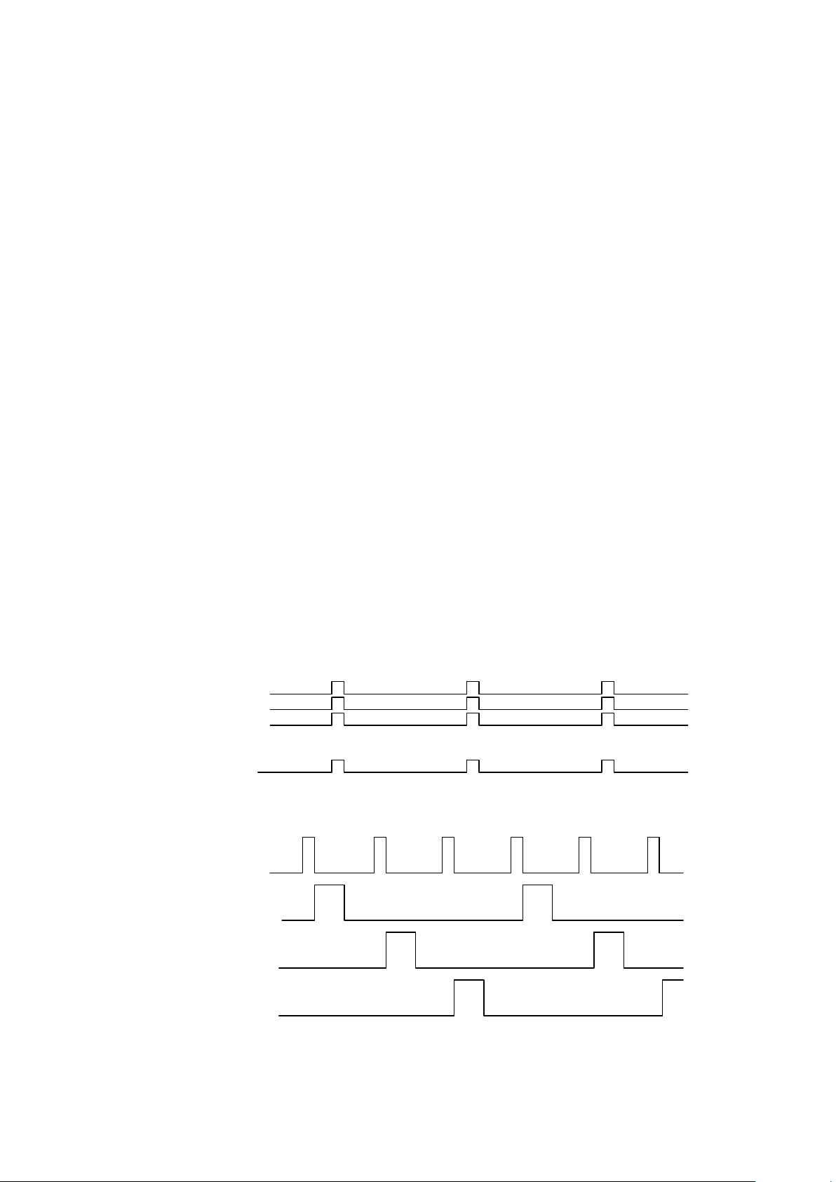
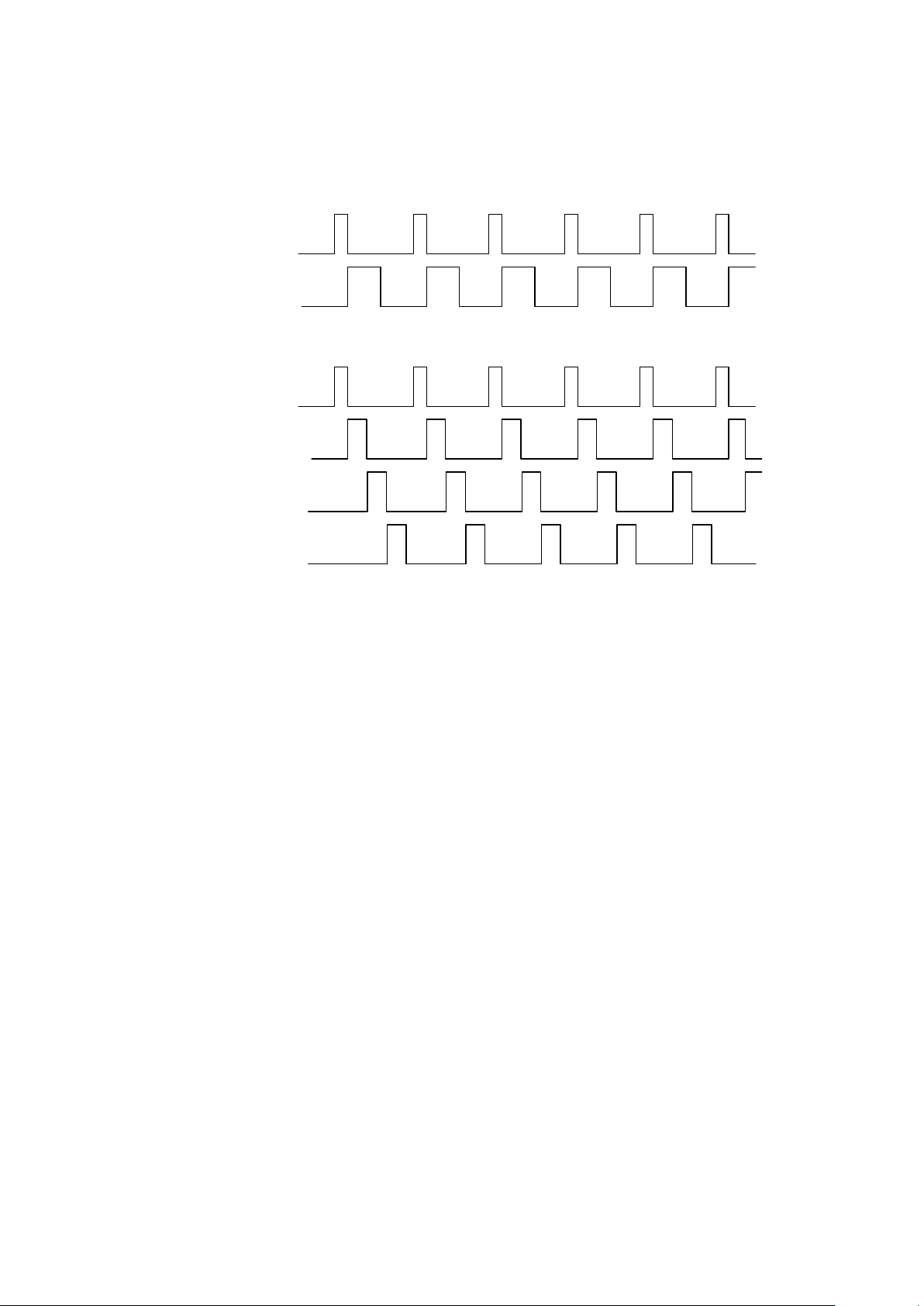
6.5 Scanning Type
Support three line in(parallel ) for CCD, one line in for CIS two types.
A. CCD
a. Three line in :
R
G
B
b. Line by line :
R G B
B. CIS
a. color scan :
TG
LED R
LED G
LED B
Page 16
GL841 USB 2.0 2-i n -1 Scanner Contr ol ler
Version 1.6
16
b. gray scan:
TG
LED R/G/B
c. true gray scan:
TG
LED R
LED G
LED B
6.6 Image Sensor Timing
Can be programmed.
A. CCD : support 600,1200 or 2400 dpi CCD.
For example NEC, TOSHIBA, Sony ……etc.
B. CIS : support 600,1200 or 2400 dpi CIS.
For example Toshiba , Canon……etc.
6.7 Dummy Line
Support programmable dummy lines to resolve (overcome) Start/Stop problem.
You can insert dummy lines to reduce scanner stop and wait events (buffer full) or always non-stop.
A. Line base of dummy lines:
The range of dummy lines is 0 line ~ 15 lines.
B. Adjustable dummy line:
The range is CCD or CIS minimum shift out time to 2096k pixels time , which can be adjusted by
1 pixel time increment.
6.8 Analog Front End Timing
External 16 bits Front-End for Wolfson WM8192, WM8199 ……etc.
6.9 Image Type
Support color, fine gray, fine line art, fast gray and fast line art scan.
Support color filters selection for gray and line art scans. The filters include Red, Green and Blue.
Note: The scan style of fine line art, fine gray or color are the same. So fine gray or fine line art
scanning speed is slow.
Page 17

GL841 USB 2.0 2-i n -1 Scanner Contr ol ler
Version 1.6
17
The exposure time of fast line art or fast gray scan is shorter than fine line art or fine gray scan.
So, fast line art or fast gray scanning speed is high.
6.10 Bits Depth
16 x3 Bits true color , 16 bits gray level and one bit line art(Black & White).
Image data type : 16 bits , 8 bits and 1 bit data type.
6.11 Shading & Correction
a. White Shading & Dark Shading:
Internal white shading by pixel (16 bits resoluti on) and dark shading by pixel (16 bits re s olution),
can be enabled or disabled By S/W. The white shading curve is calculated by S/W.
Data arrangement: three line in mode: dark R1,white R1,dark G1,white G1,dark B1,white B1,
dark R2,white R2,dark G2,white G2,dark B2,white B2,
dark R3,white R3,dark G3,white G3,dark B3,white B3,……
one line in mode:dark R1,white data R1,dark R2,white R2,dark R3, white R3…
dark G1,white data G1,dark G2,w hi t e G2,d ar k G3, whi t e G3…
dark B1,white data B1,dark B2,white B2,dark B3,white B3…
White shading formula : 2000H x Target / (Wn-Dn) = White Gain data ----- for 8 times system
White shading formula : 4000H x Target / (Wn-Dn) = White Gain data ----- for 4 times system
For example : Target = 3FFFH Wn = 2FFFH Dn = 0040H and 8 times system operation
then White Gain = 2000H x 3FFFH / (2FFFH-0040H) = 2AE4H (1.34033 times)
b. Gamma Correction :
GAMMA correction table is calculated by S/W. The resolution is 16 bits gamma table.
Range: 0 to 64k (16 bi ts) input mapping to 0 to 255 (8 bits) output ;
Style : increment or decrement gamma curve style.
Note: If you bypass gamma correction , you can get 16 bits image data.
If you enable gamma correction , you can get 8 bits image data.
Page 18
GL841 USB 2.0 2-i n -1 Scanner Contr ol ler
Version 1.6
18
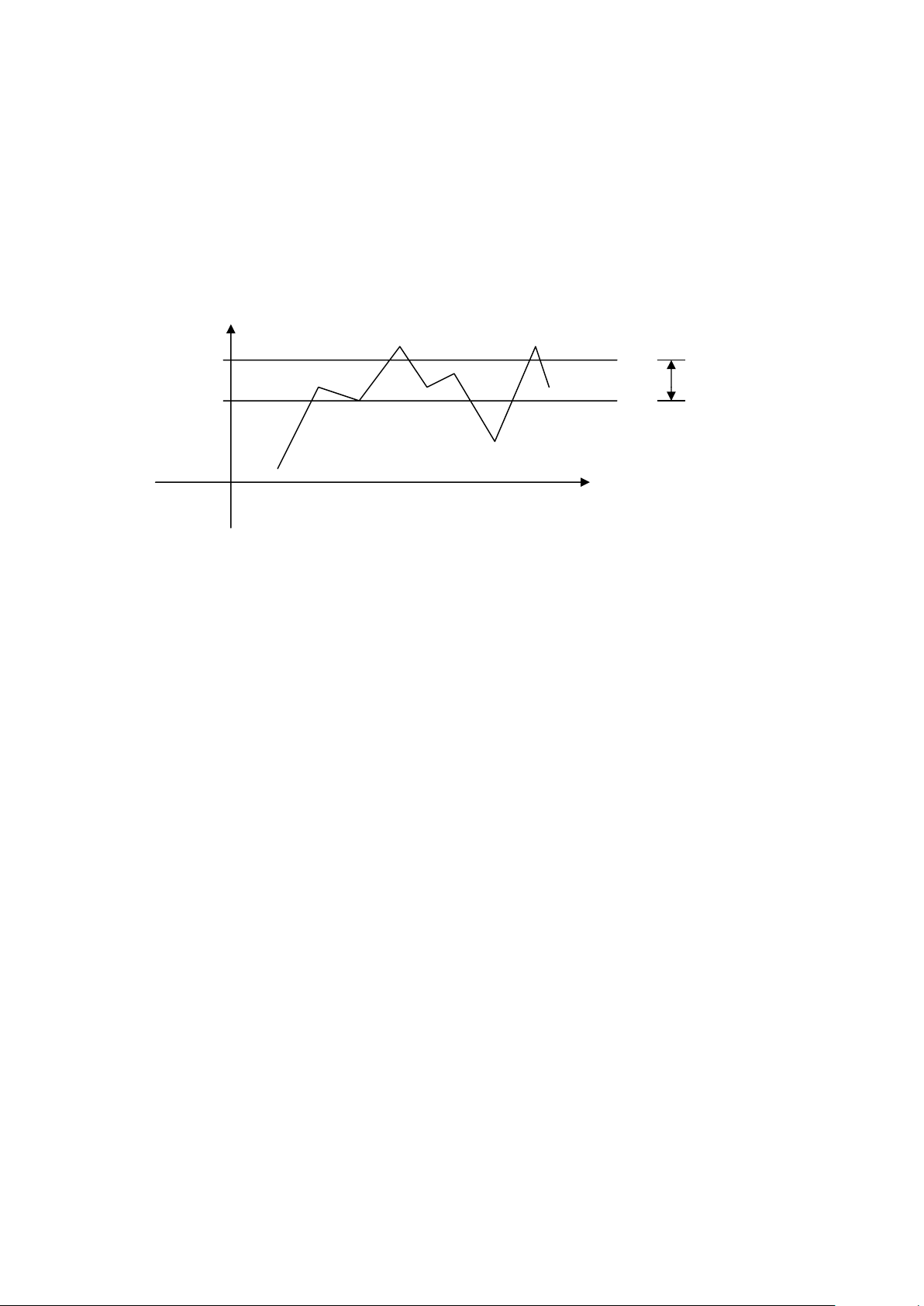
6.12 Threshold Level Setting
Can be programmed by S/W.
Range: 0 to 255 can be adjusted by one increment.
The threshold with bandwidth is in order to reduce image noise.
BWHI d h
BWLOW b c e f i bandwidth
g
a
a,b,c,g : are black pixels
d,e,f,h,i : are white pixels
6.13 Exposure Time Adjustable
Maximum: 2096k pixels time
Adjustment step: 1 pixel time.
For Transparency scan,the exposure time can up to 2096k pixel time.
6.14 Scan Width control
Scan width cont rol for horizontal line.
a.Support start pixel address, end pixel address and dummy pixel number setting
b.Maximum length: 64k pixels.
Minimum leng t h: 1 pixel
6.15 Support built-in USB(2.0)
a.Two in one: USB2.0 + scanner controller.
6.16 DRAM Timing
Support 4Mx1 , x2 Bits (256Kx16) or 16M Bits (1Mx16) for EDO DRAM ; 4M or 8M Bits for
SRAM ,as image buffer and calibration buffer timing.
You can select single or double DRAM for scanner. DRAM speed is 28ns and above for 30MHz
system clock,25ns and above for 40MHz system clock.
6.17 Horizontal Resolution Adjustable for DPI Function
A. Digital deletion type :
The resolution from 1 DPI to 2400 DPI , can be adjusted by 1 DPI increment by S/W.
B. Digital average type :
Page 19
GL841 USB 2.0 2-i n -1 Scanner Contr ol ler
Version 1.6
19
Support 1/2,1/3,1/4,1/5,1/6,1 / 8,1/10,1/12,1/15 digital average function.
For example, 1200dpi scanner: 600dpi, 400dpi, 300dpi, 240dpi, 200dpi,
150dpi, 120dpi, 100dpi, 80dpi average function.
C. Support stagger CCD :
Support 1/2,1/4 resolution , such as NEC , Toshiba and Sony stagger CCD.
6.18 Vertical Resolution Adjustable for DPI Function
The resolution of motor speed control is 16 bits, therefore we can control vertical resolution.
By one dpi increment, the resolution can be from 1 DPI to 4800DPI for 1200DPI scanner; and 1 DPI
to 9600 DPI for 2400dpi scanner.
Note: The resolution of quarter step can up to four times resolution.
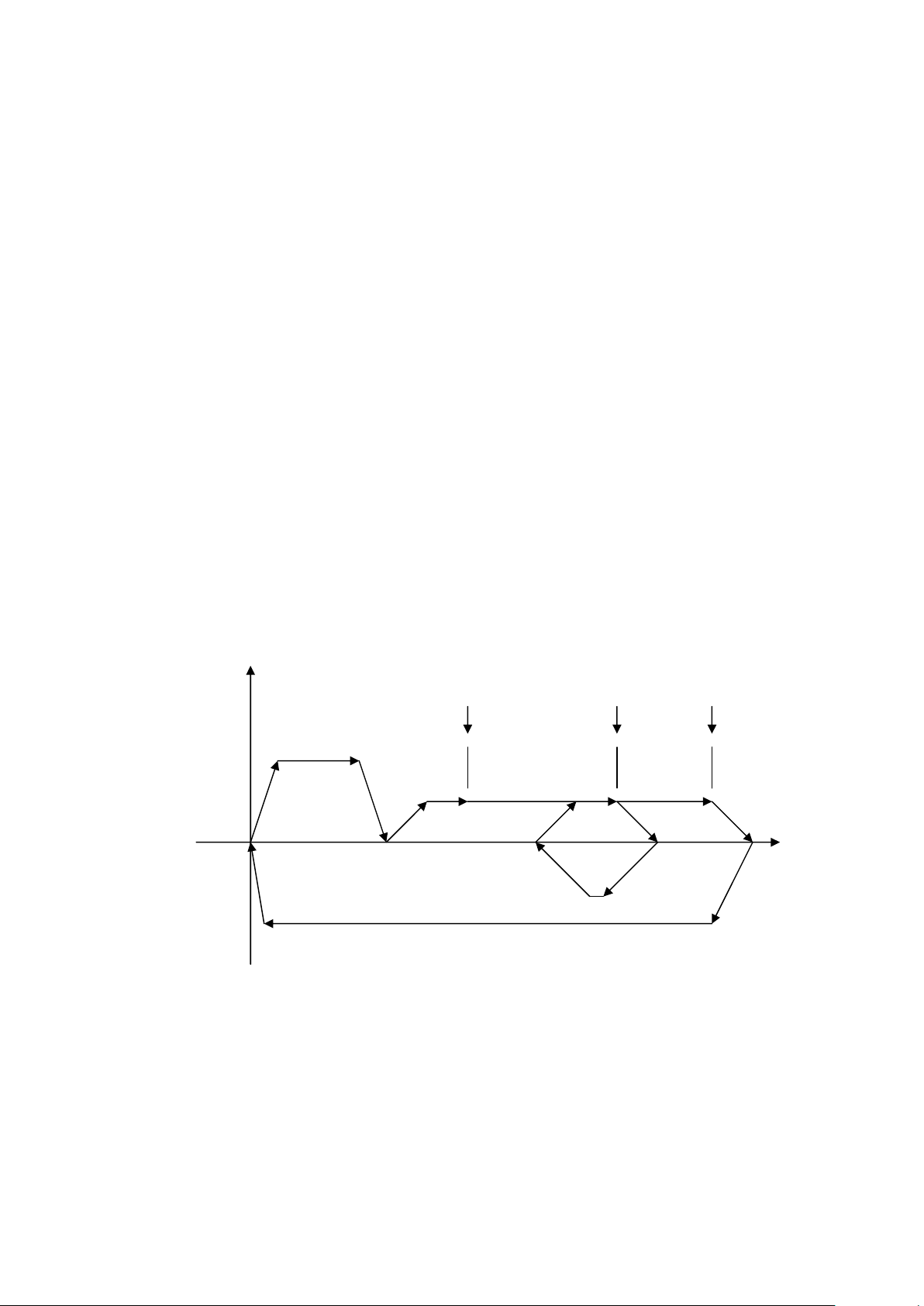
6.19 Acceleration/Deceleration Five Table
The acceleration/deceleration slope tables are stored in DRAM, can be download by S/W.
The slope can be programmed by S/W for each table. Resolution is 16 bits pixel-time. The number of
slope steps is 1~512 steps. There are five tables for motor moving. Three tables are for scanning and
the others are for fast moving. The forward and backward steps can be programmed by S/W. The
resolution is 16 bits pixel-time. The number of slope steps is 1~512 steps. You can adjust any nonlinear curve.
Note: what is fast move? Such as move back to go- home or move to scan window in any position .
(1). Two tables go to scan:
speed Scanning position buffer full position scan finished
Go to scan window
A(4) B(4) forward
C(1) D(1) E(1) F(3)
time
G(5),K H(2) I(2) J(4)
backward
go home
A,J : table four (slope four) acceleration curve for fast moving.
B : table four (slope four) deceleration curve for fast moving.
C,D : table one (slope one) acceleration curve for scanning forward.
F : table three (slope three) deceleration curve for scanning finish.
I : table two (slope two) acceleration curve for scanning backward.
H : table two (slope two) deceleration curve for scanning backward.
G : table five (slope five) deceleration curve for go-home.
K : touch home sensor deceleration curve for go-home.
Page 20
GL841 USB 2.0 2-i n -1 Scanner Contr ol ler
Version 1.6
20
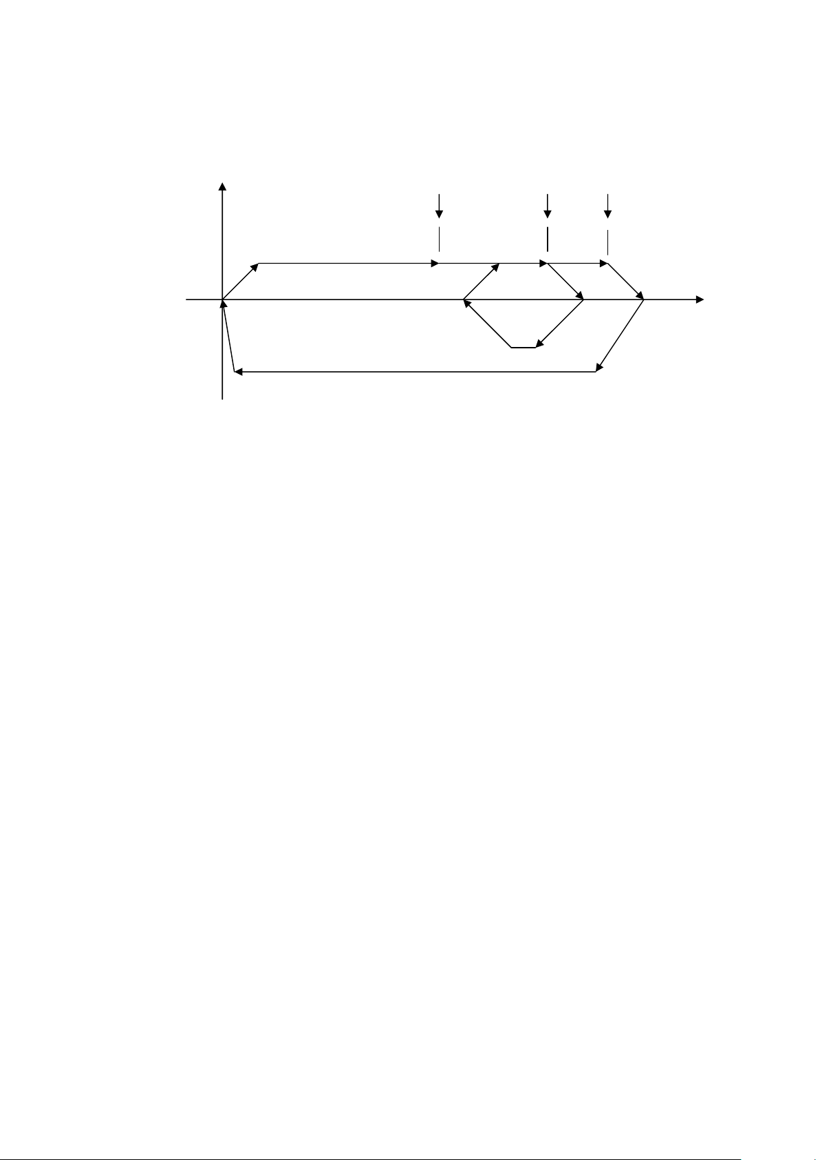
(2). One tables go to scan:
speed Scanning position buffer full position scan finished
go to scan window
C(1) D(1) E(1) F(3)
time
G(5),K H(2) I(2) J(4)
Go home
J : table four (slope four) acceleration curve for fast moving.
C,D : table one (slope one) acceleration curve for scanning forward.
F : table three (slope three) deceleration curve for scanning finish.
I : table two (slope two) acceleration curve for scanning backward.
H : table two (slope two) deceleration curve for scanning backward.
G : table five (slope five) deceleration curve for go-home.
K : touch home sensor deceleration curve for go-home.
6.20 Stepping Motor Phase Control
There is 8 output control pins to control stepping motor.mtr_ph0~7 for bi-polar and mtr_ph0~3 for
Uni-polar.
A. bi-polar :
a. Support 2916 motor driver timing and 2916 compatible driver IC, such as L6219.
Include full, half and quarter step control.
b. Support 3955 motor driver timing.
Include full, half, quarter and eighth step control.
c. Support LB1939,LB1940 motor driver timing.
Include full and half step control.
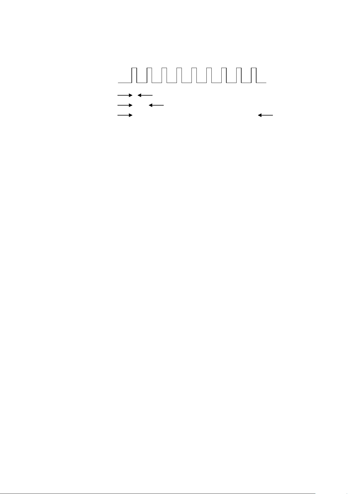
B. uni-polar :
a. Support 2003 motor driver timing and 2003 compatible driver IC.
b. Include full step two phases on, full step single phase on and half step.
c. PWM control, include frequency and duty control.
Page 21
GL841 USB 2.0 2-i n -1 Scanner Contr ol ler
Version 1.6
21
PWM
Duty
Frequency
Phase on time
6.21 Watch-Dog Protection
This function can automatically reset the system to initial state, whenever the system is held (no
access signal ) beyond the time limit.Be able to enable or disable this function by S/W.
This function can protect motor power, lamp power and A SIC system.
Calculation formula : (30sec.) x (times setting) x (setting no.).
The range of setting no. is 1~15;the range of times setting is 0~1.
6.22 Lamp Timeout Control
This circuitry can automatically reset the lamp power, whenever the system is setting. Be able to
enable or disable this function by S/W.
Calculation formula: (60sec.) x (times setting) x (setting no.).
The range of setting no. is 1~7;the range of times setting is 0~3.
6.23 Lamp Power Control
These are two power control ports for lamp. One is for Flatbed and the other is for XPA
(Transparency or film).
The resolution of its PWM type is 8 bits. Duty range is 1/256~256/256.
Note : carrier frequency is (system clock)/256.
6.24 Sensor Input
The system support home sensor input port.
6.25 16 GPIO ports
You can set input or output for each GPIO pin of the GPIO1~16 separately.
Such as keypads inputs, document sensor for sheet-fed or motor power control…etc.
Note : there are two pins for special function. One is GPIO12 and the other is GPIO11.
GPIO12 : 1. Pull up by resister to indicate that ASIC turn on lamp power whenever power on
initial.
2. Pull down by resister to indicate that ASIC turn off lamp power whenever power
on initial.
3. This pin can control bi-polar motor driver 2916,6219,3966 or 3955 Vref in order to
control Imax. current.
GPIO11 : This pin can control bi-polar motor driver 2916,6219,3966 or 3955 Vref in order to
control Imax. current.
Page 22

GL841 USB 2.0 2-i n -1 Scanner Contr ol ler
Version 1.6
22
6.26 GPO17~18 ports or Motor MTR_PH6~7 two Phase
You can select 2 pins for 3955 2 phase MTR _PH6~7 output or GPO17~18 output.
6.27 GPO13 Port or Motor Trigger signal for ADF
Motor trigger signal for ADF motor moving ,It can be controlled under scanning condition.
6.28 Power on Check
The default status of the PWRBIT is reset. You can set the PWRBIT and then read back the status in
order to check the power status. This operation is able to check first time power on or not.
6.29 RAM Test
S/W can test DRAM/SRAM IC by writ ing and reading back for checking.
6.30 LED Blinking
Support LED- blinking function. It is implemented in GPIO13~18 pins.
6.31 Support Back Scanning
Support forward or Backword scanning type.
Page 23
GL841 USB 2.0 2-i n -1 Scanner Contr ol ler
Version 1.6
23
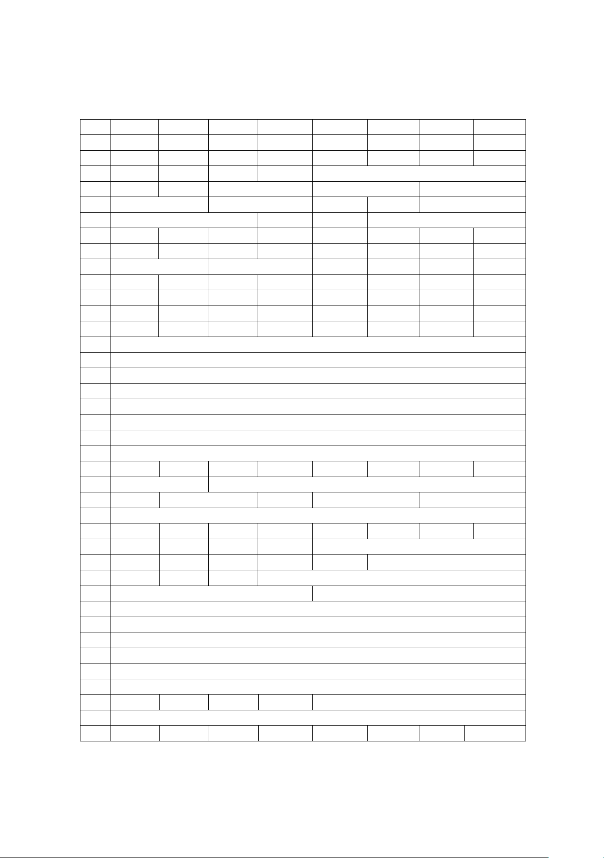
7 COMMAND SET DESCRIPTION
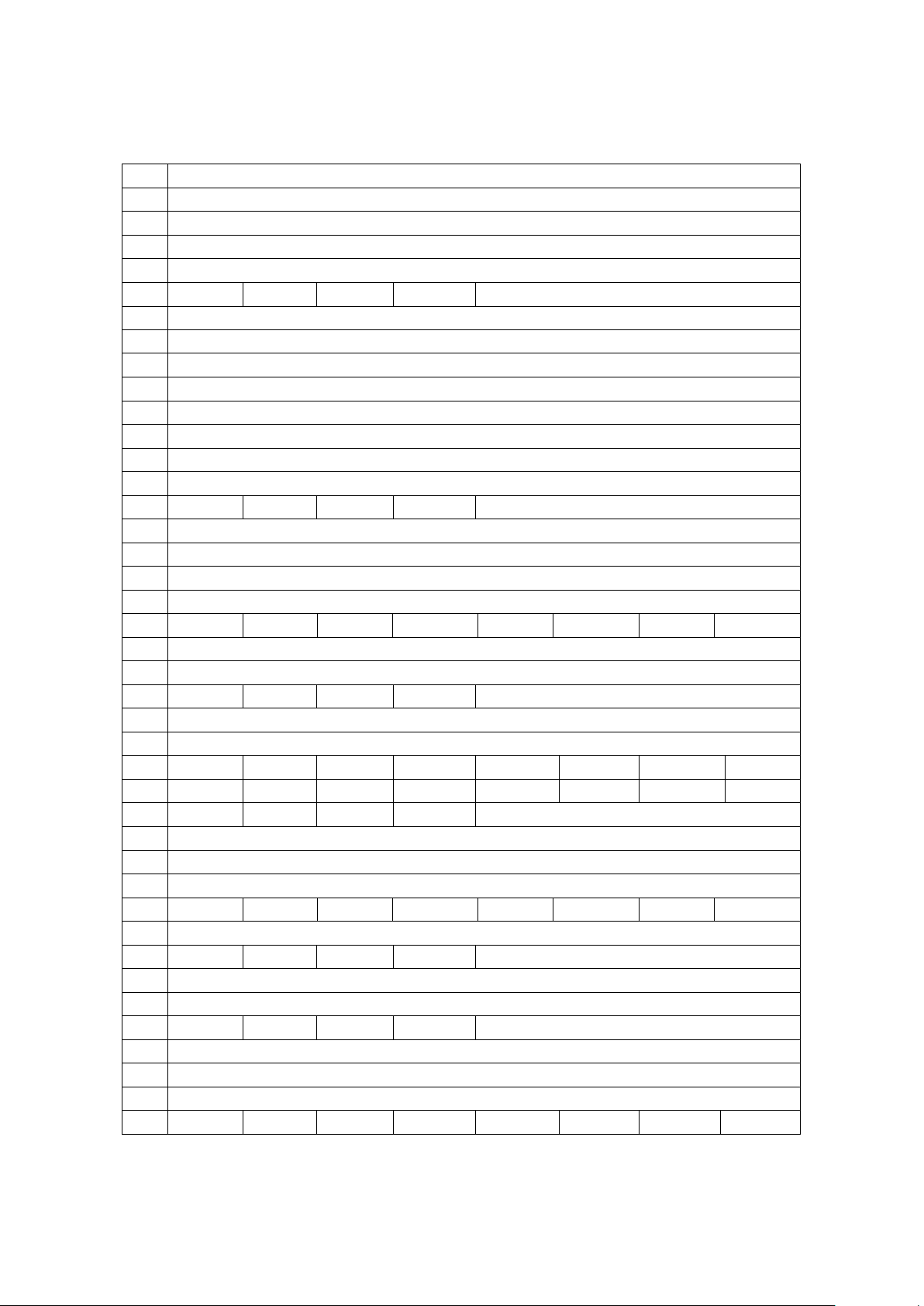
Reg. Bit7 Bit6 Bit5 Bit4 Bit3 Bit2 Bit1 Bit0
01 CISSET DOGENB DVDSET M16DRAM DRAMSEL SHDAREA S CAN
02 NOTHOME ACDCDIS AGOHOME MTRPWR FASTFED MTRREV HOMENEG LONGCURV
03 LAMPDOG AVEENB XPASEL LAMPPWR LAMPTIM[3:0]
04 LINEART BITSET AFEMOD[1:0] FILTER[1:0] FESET[1:0]
05 DPIHW[1:0] MTLLAMP[1:0] GMMENB MTLBASE[1:0]
06 SCANMOD[2:0] PWRBIT GAIN4 OPTEST[2:0]
07 SRAMSEL FASTDMA DMASEL DMARDWR
08 DECFLAG GMMFFR GMMFFG GMMFFB GMMZR GMMZG GMMZB
09 MCNTSET[1:0] CLKSET[1:0] BACKSCAN ENHANCE SHORTTG NWAIT
0A SRAMBUF
0B
0C
0D CLRLNCNT
0E SCANRESET
0F MOVE
10 EXPR[15:8]
11 EXPR[7:0]
12 EXPG[15:0]
13 EXPG[7:0]
14 EXPB[15:8]
15 EXPB[7:0]
16 CTRLHI TOSHIBA TGINV CK1INV CK2INV CTRLINV CKDIS CTRLDIS
17 TGMODE[1:0] TGW[5:0]
18 CNSET DCKSEL[1:0] CKTOGGLE CKDELAY[1:0] CKSEL[1:0]
19 EXPDMY[7:0]
1A MANUAL3 MANUAL1 CK4INV CK3INV LINECLP
1B
1C CK4MTGL CK3MTGL CK1MTGL CKAREA MTLWD TGTIME[2:0]
1D CK4LOW CK3LOW CK1LOW TGSHLD[4:0]
1E WDTIME[3:0] LINESEL[3:0]
1F SCANFED[7:0]
20 BUFSEL[7:0]
21 STEPNO[7:0]
22 FWDSTEP[7:0]
23 BWDSTEP[7:0]
24 FASTNO[7:0]
25 LINCNT[19:16]
26 LINCNT[15:8]
Reg. Bit7 Bit6 Bit5 Bit4 Bit3 Bit2 Bit1 Bit0
Page 24
GL841 USB 2.0 2-i n -1 Scanner Contr ol ler
Version 1.6
24
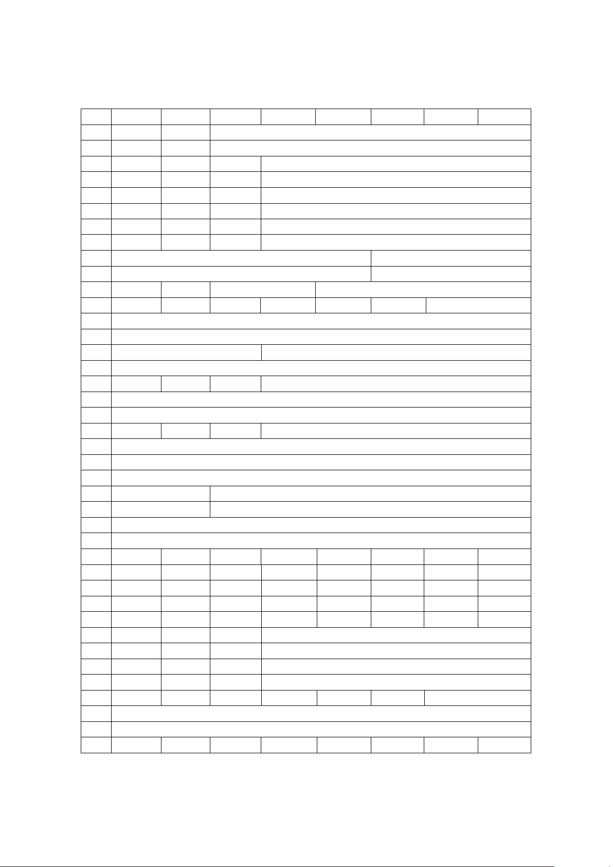
27 LINCNT[7:0]
28 “GMMWRDATA”
29 LAMPPWM[7:0]
2A RAMADDR[15:8]
2B RAMADDR[7: 0]
2C DPISET[11:8]
2D DPISET[7:0]
2E BWHI[7:0]
2F BWLOW[7:0]
30 STRPIXEL[15:8]
31 STRPIXEL[7:0]
32 ENDPIXEL[15:8]
33 ENDPIXEL[7:0]
34 DUMMY[7:0]
35 MAXWD[19:16]
36 MAXWD[15:8]
37 MAXWD[7:0]
38 LPERIOD[15:8]
39 LPERIOD[7:0]
3A FEWRDATA[8]
3B FEWRDATA[7:0]
3C “RAMWRDATA”
3D FEEDL[19:16]
3E FEEDL[15:8]
3F FEEDL[7:0]
40 HISPDFLG MOTMFLG DATAENB
41 PWRBIT BUFEMPTY FEEDFSH SCANFSH HOMESNR LAMPSTS FEBUSY MOTORENB
42 VALIDWORD[19:16]
43 VALIDWORD[15:8]
44 VALIDWORD[7:0]
45 “RAMRDDATA”
46 FERDDATA[8]
47 FERDDATA[7:0]
48 FEDCNT[19:16]
49 FEDCNT[1 5:8]
4A FEDCNT[7:0]
4B SCANCNT[19:16]
4C SCANCNT[15:8]
4D SCANCNT[7:0]
4E “GMMRDDATA”
Reg. Bit7 Bit6 Bit5 Bit4 Bit3 Bit2 Bit1 Bit0
Page 25
GL841 USB 2.0 2-i n -1 Scanner Contr ol ler
Version 1.6
25
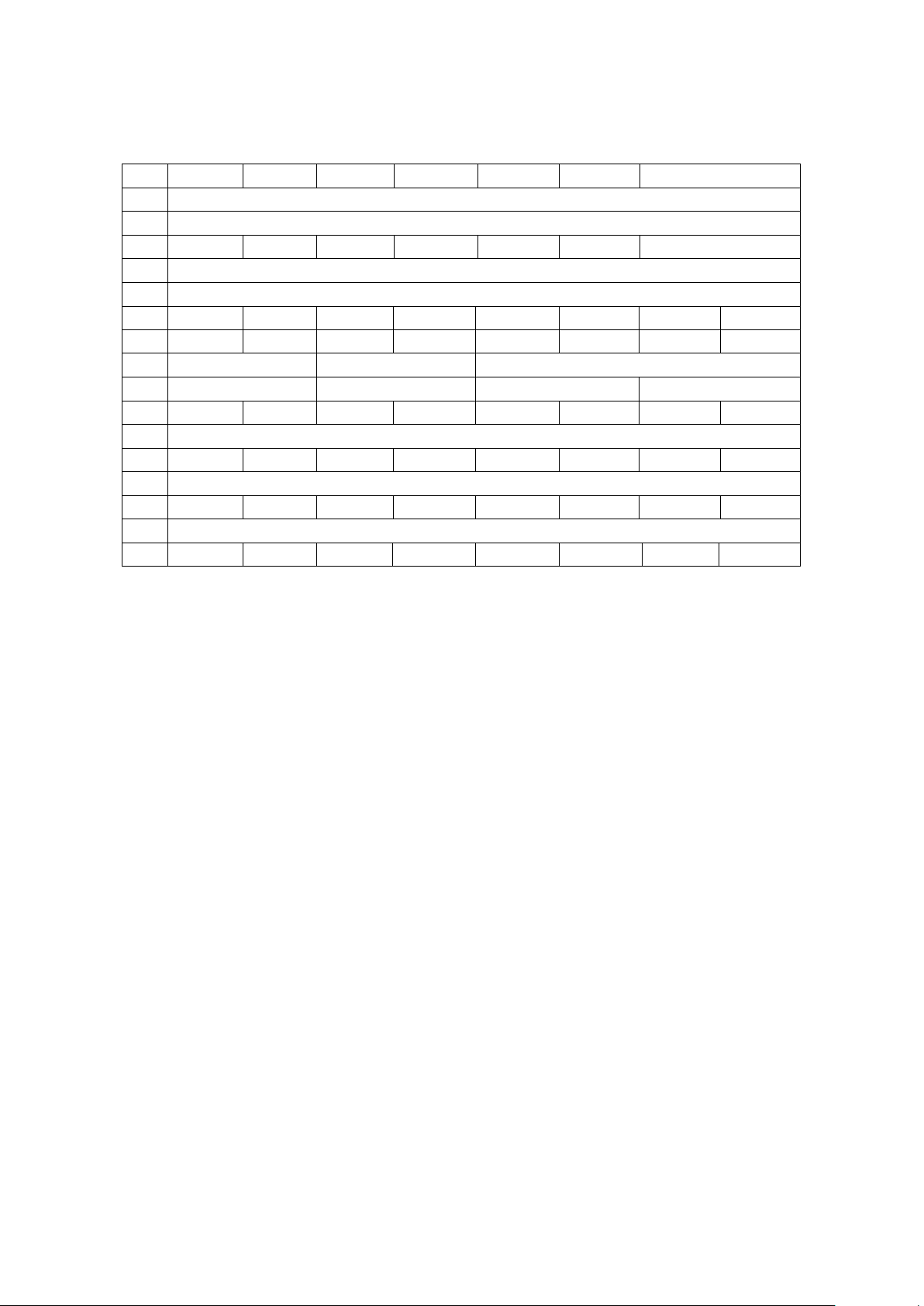
4F
50 FERDA[5:0]
51 FEWRA[5:0]
52 RHI[4:0]
53 RLOW[4:0]
54 GHI[4:0]
55 GLOW[4:0]
56 BHI[4:0]
57 BLOW[4:0]
58 VSMP[4:0] VSMPW[2:0]
59 BSMP[4:0] BSMP[2:0]
5A ADCLKINV RLCSEL CDSREF[1:0] RLC[3:0]
5B GMMADDR[9:8]
5C GMMADDR[7:0]
5D HISPD[7:0]
5E DECSEL[2:0] STOPTIM[4:0]
5F FMOVDEC[7:0]
60 Z1MOD[20:16]
61 Z1MOD[15:8]
62 Z1MOD[7:0]
63 Z2MOD[20:16]
64 Z2MOD[15:8]
65 Z2MOD[7:0]
66 PHFREQ[7:0]
67 STEPSEL[1:0] MTRPWM[5:0]
68 FSTPSEL[1:0] FASTPWM[5:0]
69 FSHDEC[7:0]
6A FMOVNO[7:0]
6B MULTFILM GPOM13 GPOM12 GPOM11 GPO18 GPO17
6C GPIO16 GPIO15 GPIO14 GPIO13 GPIO12 GPIO11 GPIO10 GPIO9
6D GPIO8 GPIO7 GPOI6 GPIO5 GPIO4 GPIO3 GPIO2 GPIO1
6E GPOE16 GPOE15 GPOE14 GPOE13 GPOE12 GPOE11 GPOE10 GPOE9
6F GPOE8 GPOE7 GPOE6 GPOE5 GPOE4 GPOE3 GPOE2 GPOE1
70 RSH[4:0]
71 RSL[4:0]
72 CPH[4:0]
73 CPL[4:0]
74 CK1MAP[17:16]
75 CK1MAP[15:8]
76 CK1MAP[7:0]
Reg. Bit7 Bit6 Bit5 Bit4 Bit3 Bit2 Bit1 Bit0
Page 26
GL841 USB 2.0 2-i n -1 Scanner Contr ol ler
Version 1.6
26
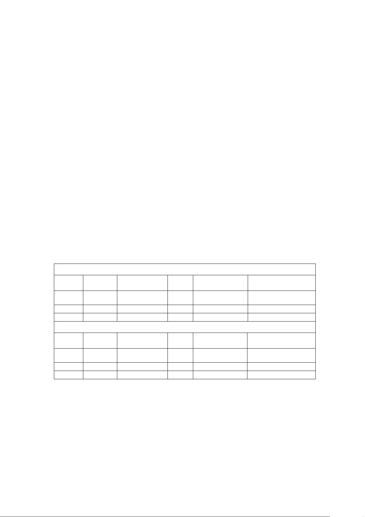
77 CK3MAP[17:16]
78 CK3MAP[15:8]
79 CK3MAP[7:0]
7A CK4MAP[17:16]
7B CK4MAP[15:8]
7C CK4MAP[7:0]
7D CK1NEG CK3NEG CK4NEG RSNEG CPNEG BSMPNEG VSMPNEG DLYSET
7E GPOLED18 GPOLED17 GPOLED16 GPOLED15 GPOLED14 GPOLED13
7F BSMPDLY[1:0] VSMPDLY[1:0] LEDCNT[3:0]
80 VRHOME[1:0] VRMOVE[1:0] VRBACK[1:0] VRSCAN[1:0]
81 ROFFSET[8]
82 ROFFSET[7:0]
83 GOFFSET[8]
84 GOFFSET[7:0]
85 BOFFSET[8]
86 BOFFSET[7:0]
87 YENB YBIT ACYCNRLC ENOFFSET LEDADD CK4ADC AUTOCONF
1. Reg : 01H (Read/Writ e)
Default : 00H
B7:CISSET : set: CIS scan type.
: reset: CCD scan type.
B6:DOGENB : set: enable watch dog of ASIC(set time out:Reg1E[7:4]).
: reset: disable.
B5:DVDSET : set : enable shading (include whole line shading and
area shading two kinds).
: reset : disable shading.
B4 : Reserved.
B3: M16DRAM : set: to select 16M bits DRAM (1M * 16).
: reset: to select 4M or 8M bits DRAM(256*16).
B2:DRAMSEL : set : the DRAM size is 4Mx2 (256kx16x2) bits.
: reset : the DRAM size is 4Mx1(256kx16x1) bits.
B1:SHDAREA :set: enable shading area (depend on scan area and scan dpi).
: reset: shading area is whole line.
B0:SCAN : set: enable scan process.
: reset: disable scan process.
2. Reg : 02H (Read/Writ e)
Default : 00H
B7:NOTHOME : set: auto-go-home doesn’t go back to home position.
: reset: go back to home position automatically.
B6:ACDCDIS : set: disable forward/backward moving whenever buffer full.
: reset: enable forward/backward moving whenever buffer full.
B5:AGOHOME : set: whenever scan is finished, carriage go home automatically.
: reset: disable auto-go-home function.
B4:MTRPWR : set: turn on MOTOR power and phase.
: reset: turn off MOTOR power and phase.
B3:FASTFED : set: enable two table for motor moving of the acceleration/deceleration.
: reset: disable two table, only use single table.
Page 27
GL841 USB 2.0 2-i n -1 Scanner Contr ol ler
Version 1.6
27
B2:MTRREV : set: set motor reverse moving.
: reset: set motor forward moving.
B1:HOMENEG : set: to indicate whenever home sensor change from high to low (falling edge) then motor
is decelerated.
Reset: to indicate whenever home sensor change from low to high (rising edge) then
motor is decelerated.
B0:LONGCURV : set: the deceleration curve of the fast moving is table 5.
: reset: the deceleration curve of the fast moving is table 4.
3. Reg : 03H (Read/Writ e)
Default : 0CH
B7:LAMPDOG : set: to start lamp sleeping mode(default on).
: reset: to disable lamp sleeping mode.
B6:AVEENB : set: select dpi average function
: reset: select dpi deletion function.
B5:XPASEL : set: select transparency lamp on.
: reset: select flatbed lamp on.
B4:LAMPPWR : set: turn on LAMP power.
: reset: turn off LAMP power.
B3~0:LAMPTIM[3:0] : lamp on time setting (default: 4)
The unit is minute.
4. Reg : 04H (Read/Writ e)
Default : 00H
B7:LINEART : set: Black/White scan.
: reset: Color/Gray scan.
B6:BITSET : set : 16 bits image data type (= word).
: reset : 8 bits image data type (= byte).
B5~4: AFEMOD[1:0] : to indicate AFE operation mode.
Wolfson Type
AFEMOD SCANMOD Description CDS
Available
Max Sample Rate Timing Requirements
2 2 Slow color
Pixel-by-pixel
Yes 5MSPS *3 channel MCLK:VSMP Rate is 8:1
1 0,1,3,4,5,6 Color pixel-by-pixel Yes 6.67MSPS *3 channel MCLK:VSMP Rate is 6:1
0 0,1,4,5,6 Fast Mono Yes 13.3MSPS *1 channel MCLK:VSMP Rate is 3:1
Analog Device Type
AFEMOD SCANMOD Description CDS
Available
Max Sample Rate Timing Requirements
2 0,1,4,5,6 Slow color
Pixel-by-pixel
Yes MCLK:VSMP Rate is 3:1
1 0,1,2,3,4,5,6 Mono Yes MCLK:VSMP Rate is 2:1
0 0,1,2,3,4,5,6 Fast Mono Yes MCLK:VSMP Rate is 1:1
B3~2:FILTER[1:0] : scan color type : a.00: color
b.01: R
c.10: G
d.11: B
B1~0:FESET[1:0] : front end operation type: a.00: ESIC type 1.
b.01: ESIC type 2.
c.10: ADI type.
d.11: reserved.
5. Reg : 05H (Read/Writ e)
Default:00H
Page 28

GL841 USB 2.0 2-i n -1 Scanner Contr ol ler
Version 1.6
28
B7~6: DPIHW[1:0] : set CCD/CIS resolution
00=600dpi
01=1200dpi
10=2400dpi
11=reserved.
B5~4: MTLLAMP[1:0] : to set times of the lamp time out.
00: 1* LAMPTIM
01: 2*LAMPTIM
10: 4*LAMPTIM
11: reserved.
B3: GMMENB : set: enable gamma correction.
: reset: bypass gamma correction.
B2: Reserved.
B1~0: MTLBASE[1:0] : to set output CCD pixel number under each system pixel time.
00=1 CCD pixel/system pixel time.
01=2 CCD pixels/system pixel time.
10=3 CCD pixels/system pixel time.
11=4 CCD pixels/system pixel time.
6. Reg : 06H (Read/Writ e)
Default:00H
B7~5: SCANMOD[2:0] : set scan operation mode
000:12 clocks/pixel ; normal mode operation for scanning.
Include color(pixel rate),fine gray and fine line-art.
001:12 clocks/pixel ; bypass mode operation for calibration.
Include color(pixel rate) and fine gray.
010:reserved.
011:reserved.
100:6 clocks/pixel ; fast mode operation.
Include color(line rate),fast gray and fast line-art.
101:15 clocks/pixel ; for 16 bits color output.
110:18 clocks/pixel ; for 16 bits color output.
B4: PWRBIT :When power on,set this bit.To indicate power has on.
Default is reset.
B3: GAIN4 : set: digital shading gain=4 times system.
: reset: dig ital shading gain=8 times system.
Note: If you want to get more precise image quality,you can set GAIN4 bit.
B2~0: OPTEST[2:0]: select ASIC operation type.
000: set normal mode to capture AFE image.
001: set DRAM bank,power on carriage initiated and
ADF(motortgo) test for ASIC simulation.
010: pixel count pattern for ASIC image test.
011: line count pattern for ASIC image test.
100: counter and adder test for ASIC simulation t est.
7. Reg : 07H (Read/Writ e)
Default:00H
B3:SRAMSEL : set: DMA access for SRAM.
: reset: DMA access for DRAM.
B2:FASTDMA : set: 2clocks/access,that is to say 2clocks/16bits or 2clocks/8bits for DMA access.
: reset: 4clocks/access,that is to say 4clocks/16bits or 4clocks/8bits for
DMA access.
B1:DMASEL : set: DMA access DRAM under command mode.
: reset: MPU access DRAM under command mode.
B0:DMARDWR : set: DMA read DR AM under command mode.
Page 29

GL841 USB 2.0 2-i n -1 Scanner Contr ol ler
Version 1.6
29
: reset: DMA write DRAM under command mode.
Note: DMA operation can be processed under CPU and DMA type.
8. Reg : 08H (Read/Writ e)
Default:00H
B6: DECFLAG : set :gamma table is decrement type
: reset :gamma table is increment type.
B5: GMMFFR : set: to indicate that red channel Gamma table address FFH is special value.
B4: GMMFFG : set: to indicate that red channel Gamma table address FFH is special value.
B3: GMMFFB : set: to indicate that red channel Gamma table address FFH is special value.
B2: GMMZR : set: to indicate that red channel Gamma table address 00H is special value.
B1: GMMZG : set: to indicate that green channel Gamma table address 00H is special value.
B0: GMMZB : set: to indicate that blue channel Gamma table address 00H is special value.
9. Reg : 09H (Read/Writ e)
Default:00H
B7~6: MCNTSET[1:0] : to select the unit of motor table counter.
00: pixel count.
01:system clock*2.
10:system clock*3.
11:system clock*4.
B5~4: CLKSET[1:0] : to select the system clock frequency.
00: 24MHz
01: 30MHz
10: 40MHz
11:48MHz.
B3: BACKSCAN : set: to enable backward scan function.
: reset: to select forward scan function.
B2: ENHANCE : set: to enhance EPP interface speed for USB2.0
: reset: to select normal EPP interface speed for USB2.0
B1: SHORTTG : set: enable short CCD SH(TG) period for film scanning.
B0: NWAIT : set: to delay nWait (H_BUSY) one clock.
10. Reg : 09H (Read/Write)
Default:00H
B0: SRAMBUF :set: to select external SRAM as the image buffer.
:reset: to select external DRAM as the image buffer.
11. Reg : 0DH (Write)
Command : scanner command.
B0: CLRLNCNT : set: to clear SCANCNT(Reg4B,Reg4C,Reg4D).
: reset: don’t clear SCANCNT.
Note: For each time scanning , you must clear SCANCNT before starting process.
12. Reg : 0EH (Write)
Command : scanner software reset.
It can initiate AISC system, including lamp and motor,
Control registers, internal circuit and status, but not including tables in
DRAM, like gamma table, shading table and acceleration/deceleration table.
Note: In normal condition, it is unnecessary to reset scanner , unless the scanner is out of control.
13. Reg : 0FH (Write)
Command : motor moving.
Start motor farward/backward moving.
14. Reg : 10,11H (Read/Write)
Default : 00H,00H
Page 30
GL841 USB 2.0 2-i n -1 Scanner Contr ol ler
Version 1.6
30
EXPR[15:0]: Red-LED array of CIS or Red channel TG of CCD exposure time setting.
Note: can not be programmed to logic zero.
15. Reg : 12H,13H (Read/Write)
Default : 00H,00H
EXPG[15:0]: Green-LED array of CIS or Green channel TG of CCD exposure time setting.
Note: can not be programmed to logic zero.
16. Reg : 14H,15H (Read/Write)
Default : 00H,00H
EXPB[15:0]: Blue-LED array of CIS or Blue channel TG of CCD exposure time.
Note: can not be programmed to logic zero.
17. Reg : 16H (Read/Write)
Default : 32H
B7:CTRLHI : set: CCD CP & RS are high under TG high position.
: reset: CCD CP & RS are low under TG high position.
B6: TOSHIBA : set: to indicate the image sensor is TOSHIBA CIS.
B5:TGINV : set: to reverse CCD TG.
: reset: don’t reverse.
B4:CK1INV : set: to reverse CCD Clock 1.
: reset: don’t reverse.
B3:CK2INV : set: to reverse CCD Clock 2.
: reset: don’t reverse.
B2:CTRLINV : set: to reverse CCD CP & RS.
: reset: don’t reverse.
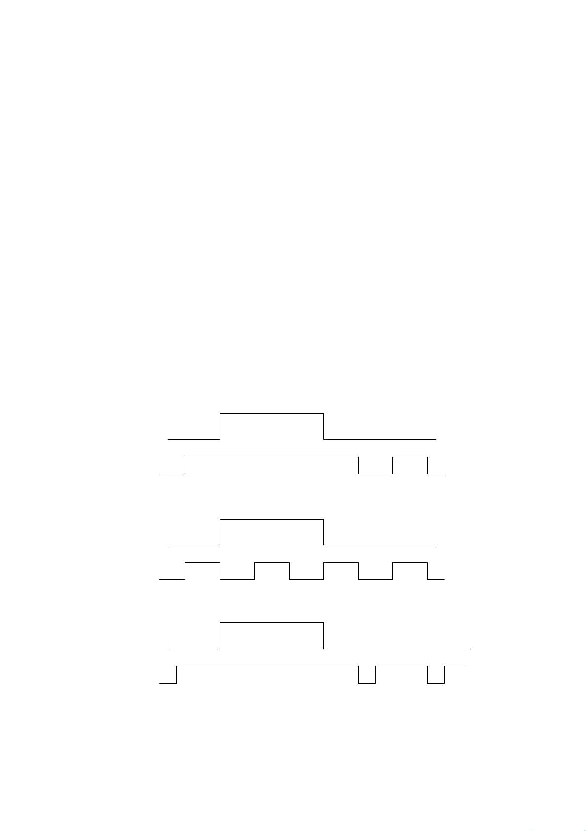
B1:CKDIS : set: disable CCD TG position Clock 1/2 signals.
CCD TG
CCD Clock
: reset: enable CCD TG position Clock 1/2 signals.
CCD TG
CCD Clock
B0:CTRLDIS : set: disable CCD TG position CP & RS signals.
CCD TG
CCD CP/RS
: reset: enable CCD TG position CP & RS signals.
Page 31

GL841 USB 2.0 2-i n -1 Scanner Contr ol ler
Version 1.6
31
CCD TG
CCD CP/RS
18. Reg : 17H (Read/Write)
Default : 14H
B7~6:TGMODE[1:0] : to set CCD TG mode.
00:without dummy line CCD TG type.
01:with reflectional d oc ument scanning type.
10:with transparency scanning type.
11:TGMODE=2 for simulation.
B5~0:TGW[5:0] : to set CCD TG width.
Note: Can not be programme d t o l ogic zero.
19. Reg : 18H (Read/Write)
Default : 00H
B7 : CNSET : set : TG and clock set to Canon CIS style.
: reset: TG and clock is non-Canon CIS style.
B6~5 :DCKSEL : 00 one time CCD Clocks speed for dummy line.
01 two times CCD Clocks speed for dummy line.
10 three times CCD Clocks speed for dummy line.
11 four times CCD Clocks speed for dummy line.
B4 :CKTOGGLE : set : half cycle per pixel for CCD Clock 1/2.
: reset : one cycle per pixel
B3~2 :CKDELAY: 0 0 no delay
01 delay one system clock for CCD Clock 1/2.
10 delay two systems clock for CCD Clock 1/2.
11 delay three systems clock for CCD Clock 1/2.
B1~0 :CKSEL : 00 one time CCD Clock speed for capture image.
01 two times CCD Clock speed for capture image.
10 three times CCD Clock speed for capture image.
11 four times CCD Clock speed for capture image.
Note : CCD Clock speed up limitation :
1. SCANMOD=0,1 : 12 cl ocks/pixel a. toggl e CCD : be able to speed up 1,2,3,4 times.
b. non-toggle CCD : be able to speed up 1,2,3 times.
2. SCANMOD=2 : reserved .
2. SCANMOD=3 : reserved .
3. SCANMOD=4 : 6 clocks/pixel a. toggle CCD : be able to speed up 1,2,3 times.
b. non-toggle CCD : can not speed up.
4. SCANMOD=5 : 15 clocks/pixel a.toggle CCD : be able to speed up 1,2,3,4 times.
b.non-toggle CCD : be able to speed up 1,2,3 times.
5. SCANMOD=6 : 18 clocks/pixel a.toggle CCD : be able to speed up 1,2,3,4 times.
b.non-toggle CCD : be able to speed up 1,2,3,4 times.
20. Reg : 19H (Read/Write)
Default : 00H
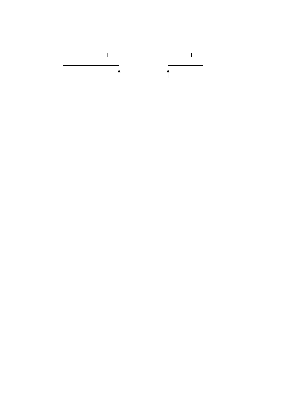
EXPDMY[7:0] : to set dummy line exposure time (unit = 256 pixels time) or CIS LED array turn-on time.
Note: the unit is pixel time.
Page 32
GL841 USB 2.0 2-i n -1 Scanner Contr ol ler
Version 1.6
32
CIS SP
CIS LED
EXPDMY for turn on EXPR/EXPG/EXPB for turn off
Note: can not be programmed to logic zero.
21. Reg : 1AH (Read/Write)
Default : 00H
B7: Reserved.
B6: Reserved.
B5:MAUNAL3 : set : CCD Clock 3,Clock4 manual output.
: reset : CCD Clock 3,Clock4 automatic output.
B4:MANUAL1 : set : CCD Clock 1,Clock2 manual output.
: reset : CCD Clock 1,Clock2 automatic output.
B3:CK4INV : set : to reverse CCD Clock4.
: reset : don’t reverse.
B2:CK3INV : set : to reverse CCD Clock 3.
: reset : don’t reverse.
B1:LINECLP : set : to select CCD line clamping.
: reset : to select CCD pixel clamping.
B0:Reserved.
22. Reg : 1BH (Read/Write)
Default : 00H
Reserved.
23. Reg : 1CH (Read/Write)
Default : 00H
B7: CK4MTGL : to indicate CCD clock 4 to use toggle function.
B6: CK3MTGL : to indicate CCD clock 3 to use toggle function.
B5: CK1MTGL : to indicate CCD clock 1 to use toggle function.
B4: CKAREA : set : CCD coloks speed depend on scan area.
B3: MTLWD : to set double of the watch-dog time out .
B2~0:TGTIME[2:0] : CCD Line Period selection. a.000: 1*LPERIOD(Reg38,Reg39)
b.001: 2*LPERIOD
c.010: 4*LPERIOD
d.011: 8*LPERIOD
e.100: 16*LPERIOD
f. 101: 32*LPERIOD
24. Reg : 1DH (Read/Write)
Default : 04H
B7 :CK4LOW : to set CCD clock4 are low under CCD TG.
B6 :CK3LOW : to set CCD clock3 are low under CCD TG.
B5: :CK1LOW : to set CCD clock1,2 are low under CCD TG.
B4~0 :TGSHLD[4:0] : to set CCD TG shoulder width.
Note: You have to program the TGSHLD >= 2 (more than two)
25. Reg : 1EH (Read/Write)
Default : 20H
B7~4:WDTIME[3:0] : to set watch-dog time
The unit is 30 seconds.
B3~0:LINESEL[3:0] : to set CIS Vertical DPI or dummy lines.
Page 33
GL841 USB 2.0 2-i n -1 Scanner Contr ol ler
Version 1.6
33
CIS : LINESEL =0 full dpi.
=1 1/2 dpi
=2 1/3 dpi
…..
=15 1/16 dpi
CCD : LINESEL =0 no dummy line.
=1 1 dummy line.
=2 2 dummy lines.
……
=15 15 dummy lines.
Note : CIS can be implemented dummy line by motor move mothod,not dummy lines.
26. Reg : 1FH (Read/Write)
Default : 00H
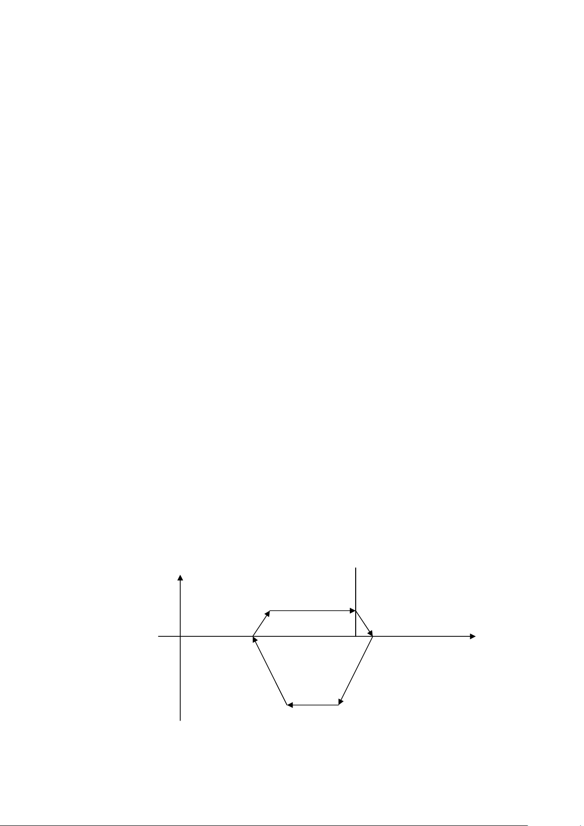
SCANFED[7:0]: move to scanning position by table one under two table operation.
Note: can not be programmed to logic zero.
27. Reg : 20H (Read/Write)
Default : 00H
BUFSEL[7:0] : to set buffer condition (unit = 4k word).
Scanner execute backward/forward moving whenever buffer full.
If MAXWD < buffer condition , then motor move forward to scan.
28. Reg : 21H (Read/Write)
Default : 00H
STEPNO[7:0]: to set scanning forward slope curve of the acceleration/deceleration (table one slope).
Note: can not be programmed to logic zero.
29. Reg : 22H (Read/Write)
Default : 00H
FWDSTEP[7:0] : to set steps number of the forward steps.
Note: can not be programmed to logic zero.
30. Reg : 23H (Read/Write)
Default : 00H
BWDSTEP[7:0] : to set steps number of the backward steps.
Note: can not be programmed to logic zero.
31. Reg : 24H (Read/Write)
Default : 00H
FASTNO[7:0]: to set scanning backward slope curve of the acceleration/deceleration (table two slope).
Buffer full position
speed
Reg22
Reg21 Reg21
time
Reg24 Reg24
Reg23
Page 34
GL841 USB 2.0 2-i n -1 Scanner Contr ol ler
Version 1.6
34
Note: can not be programmed to logic zero.
32. Reg : 25H,26H,27 H (Read/Write)
Default : 00H,00H,00H
LINCNT[19:0]: to set the scan lines number.
Note: can not be programmed to logic zero.
33. Reg : 28H (Read/Write)
Default : 00H
GMMWRDATA : this port to write gamma table.
34. Reg : 29H (Read/Write)
Default : FFH
LAMPPWM[7:0] : to set PWM duty for lamp power control.
0: 1/256 duty.
1: 2/256 duty.
…..
255:256/256 duty.
35. Reg : 2AH,2BH (Read/Write)
Default : 00H.00H
RAMADDR[15:0] : to set DRAM start address to access data.
note: IRAM_A[19:0]={RAMADDR[15:0],4’b0000}.
36. Reg : 2CH,2DH (Read/Write)
Default : 00H,00H
DPISET[10:0] : set resolution of DPI for average ty pe or deletion type.
A. average type : digital average function support 1/2,1/3,1/4,1/5,1/6,1/8,1/10,1/12,1/15.
a. 2400 dpi scanner : can set 1200,800,600,480,400,300,240,200,160 dpi.
b. 1200 dpi scanner : can set 600,400,300,240,200,150,120,100,80 dpi.
c. 600 dpi scanner : can set 300,200,150,120,100,75,60,50 and 40 dpi.
B. deletion type : 2400,1200 or 600dpi to 1 dpi setting dec r ement by one dpi.
Note: can not be programmed to logic zero.
37. Reg : 2EH (Read/Write)
Default : 00H
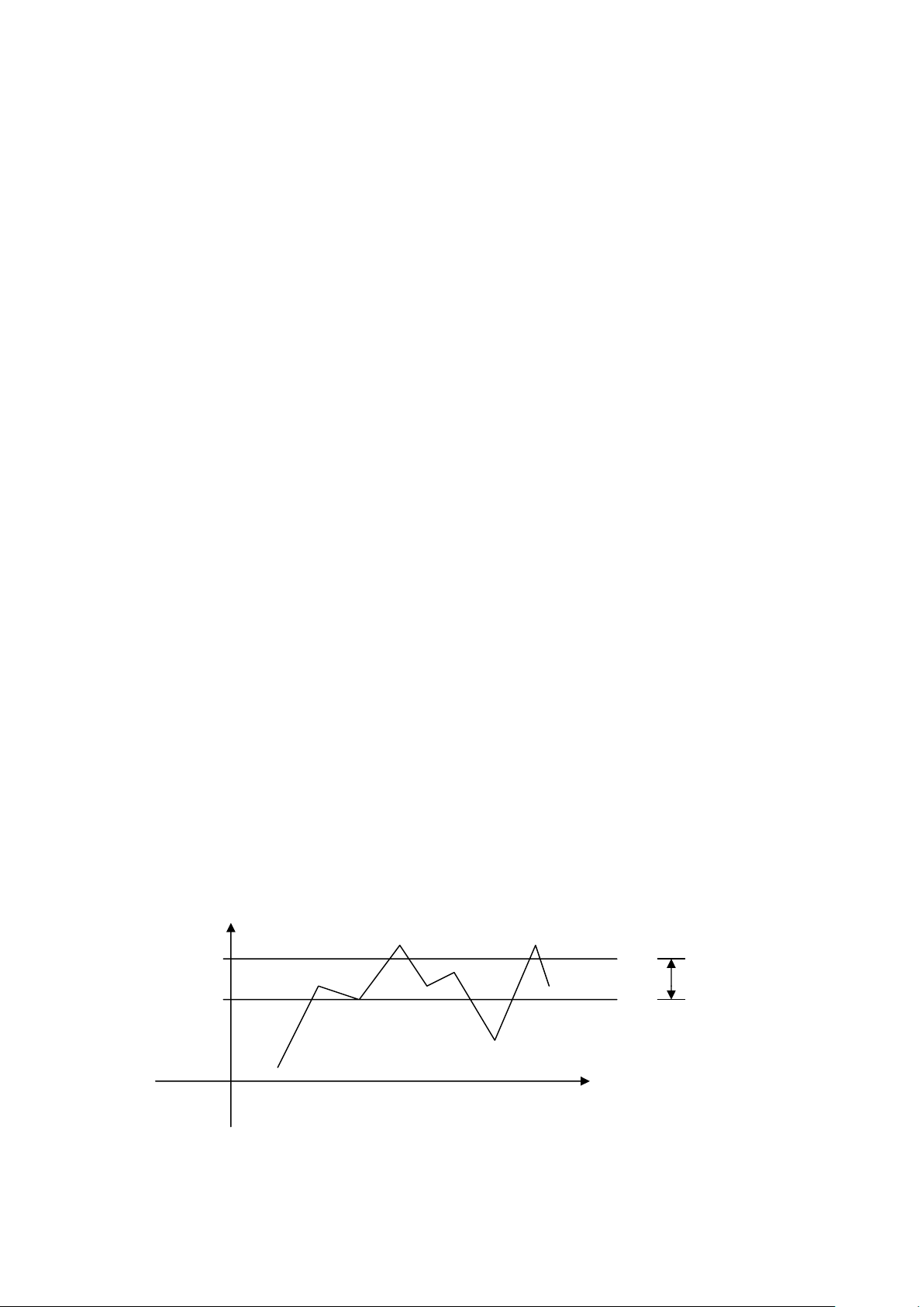
BWHI[7:0] : to set Black & White threshold high level.
38. Reg : 2FH (Read/Write)
Default : 00H
BWLOW[7:0] : to set Black & White threshold low level.
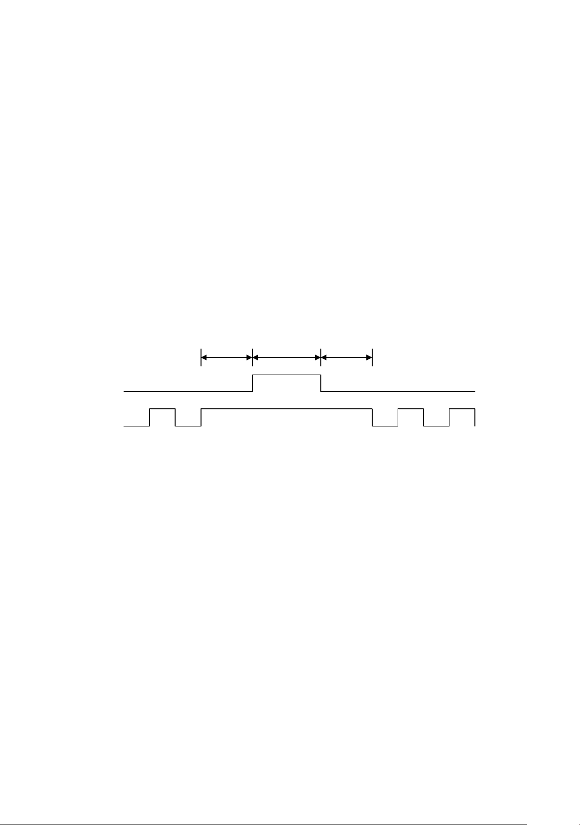
BWHI d h
BWLOW b c e f i bandwidth
g
a
Page 35
GL841 USB 2.0 2-i n -1 Scanner Contr ol ler
Version 1.6
35
a,b,c,g : are black pixels
d,e,f,h,i : are white pixels
39. Reg : 30H,31H (Read/Write)
Default : 00H,00H
STRPIXEL[15:0] : to set the begin pixel position (unit : pixel count).
STRPIXEL=(TGW+2*TGSHLD)+Begin pixels number.
Note: can not be programmed to logic zero.
40. Reg : 32H,33H (Read/Write)
Default : 00H,00H
ENDPIXEL[15:0] : to set the end pixel position (unit : pixel count).
ENDPIXEL=(TGW+2*TGSHLD)+End pixels number.
Note: can not be programmed to logic zero.
41. Reg : 34H (Write)
Default : 00H
DUMMY[7:0] : to set the CCD dummy & optical black pixels position (unit : pixel count).
Note : Reg30,31,32,33 and 34 setting rule.
TGSHLD(Reg1D) RGW(Reg17) TGSHLD(Reg1D)
CCD TG
CCD clock
CCD pixel no: N-1 N 0 1 2 3 4
For example begin pixel is 65 ,end pixel is 100 and CCD dummy pixel is 64,
Then STRPIXEL=(TGW+2*TGSHLD)+65.
ENDPIXEL=(TGW+2*TGSHLD)+100.
DUMMY =(TGW+2*TGSHLD)+64.
Note: can not be programmed to logic zero.
42. Reg : 35H,36H,37H (Read/Write)
Default : 00H,00H,00H
MAXWD[19:0] : to set maximum word size per line for ASIC estimation.
If usable buffer size < MAXWD,then buffer is full.The scanner execute forward and
Backward moving.
43. Reg : 38H,39H (Read/Write)
Default : 15H,18H
LPERIOD[15:0] : to set Line period(or exposure time) for CCD.
Unit : pixel count
Note: can not be programmed to logic zero.
44. Reg : 3AH,3BH (Read/Write)
Default : 00H,00H
FEWRDATA[8:0] : This port is used to write data to co ntrol register of front-end.
45. Reg : 3CH (Read/Write)
Default : 00H
Page 36

GL841 USB 2.0 2-i n -1 Scanner Contr ol ler
Version 1.6
36
RAMWRDATA : This port is used to write data to DRAM.
46. Reg : 3DH,3EH,3FH (Read/Write)
Default : 00H,00H,00H
FEEDL[19:0] : to set feeding steps number of motor move.
Note: can not be programmed to logic zero.
47. Reg : 40H (Read)
B2:HISPDFLG : set: motor is high-speed moving.
B1:MOTMFLG : set: motor is moving.
: reset: motor is stop.
B0:DATAENB : set: scanner is scanning mode.
Reset: scanner is command mode.
48. Reg : 41H (Read)
B7:PWRBIT : To indicate power status.
Power on initial,PWRBIT=0;
B6:BUFEMPTY : set: To indicate that the image buffer is empty.
: reset: To indicate that the image buffer is not empty.
B5:FEEDFSH : set: To indicate that motor feeding is finished.
: reset: To indicate that motor feeding is not finished.
B4:SCANFSH : set: To indicate that scan is finished.
: reset: To indicate that scan is not finished.
B3:HOMESNR : set: home sensor is off (is home position).
: reset: home sensor is on (is not home position).
B2:LAMPSTS : set: lamp is on.
: reset: lamp is off.
B1:FEBUSY : set: front end is busy and can not read/write again.
: reset: front end is ready and be able to read/write again.
B0:MOTORENB : set: motor is processing.
: reset: motor is not processing.
49. Reg : 42H,43H,44H (Read)
VALIDWORD[19:0] : to indicate available words to read out in the image buffer of DRAM.
50. Reg : 45H (Read)
RAMRDDATA : this port for read DRAM data.
51. Reg : 46H,47H (Read)
FERDDATA[8:0] : this port is used to read out data from front-end control register.
52. Reg : 48H,49H,4AH (Read)
FEDCNT[19:0] : to read motor feeding steps number.
For example,if you have set moving steps no. and execute moving command.
You can read out steps no. moved.
53. Reg : 4BH,4CH,4DH (Read)
SCANCNT[19:0] : to read scanner finished lines number.
54. Reg : 4EH (Read)
GMMRDDATA : this port to read back the gamma table.
55. Reg : 50H (Read/Write)
Default : 00H
FERDA[5:0] : this port is read address setting for Front End control register read.
Page 37
GL841 USB 2.0 2-i n -1 Scanner Contr ol ler
Version 1.6
37
56. Reg : 51H (Read/Write)
Default : 00H
FEWRA[5:0] : this port is write address setting for Front End control register write.
57. Reg : 52H,53H (Read/Write)
Default : 00H,00H
RHI[4:0] : to latch R channel high byte data of AFE.
RLOW[4:0] : to latch R channel low byte data of AFE.
58. Reg : 54H,55H (Read/Write)
Default : 00H,00H
GHI[4:0] : to latch G channel high byte data of AFE.
GLOW[4:0] : to latch G channel low byte data of AFE.
59. Reg : 56H,57H (Read/Write)
Default : 00H,00H
BHI[4:0] : to latch B channel high byte data of AFE.
BLOW[4:0] : to latch B channel low byte data of AFE.
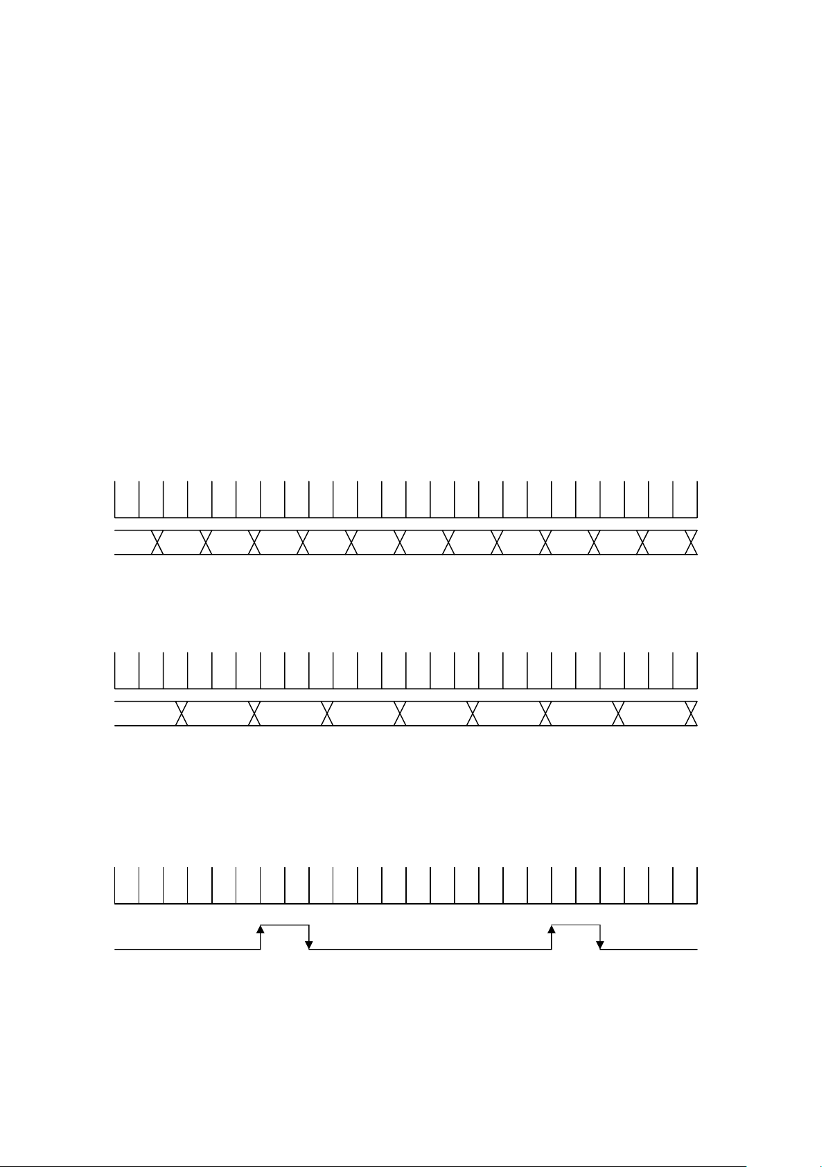
(1). Color,fine gray or fine line-art : 12 phase/pixel
0 1 2 3 4 5 6 7 8 9 10 11 0 1 2 3 4 5 6 7 8 9 10 11
R[15:8] R[7:0] G[15:8] G[7:0] B[15:8] B[7:0] R[15:8] R[7:0] G[15:8] G[7:0] B[15:8]
RHI = 01H RLOW = 03H
GHI = 05H GLOW = 07H
BHI = 09H BLOW = 11H
(2).Fast gray or fast line-art : 6 phase/pixel
0 1 2 3 4 5 0 1 2 3 4 5 0 1 2 3 4 5 0 1 2 3 4 5
R[15:8] R[7:0] R[15:8] R[7:0] R[15:8] R[7:0] R[15:8]
RHI = 02H RLOW = 05H
60. Reg : 58H (Read/Write)
Default : 00H
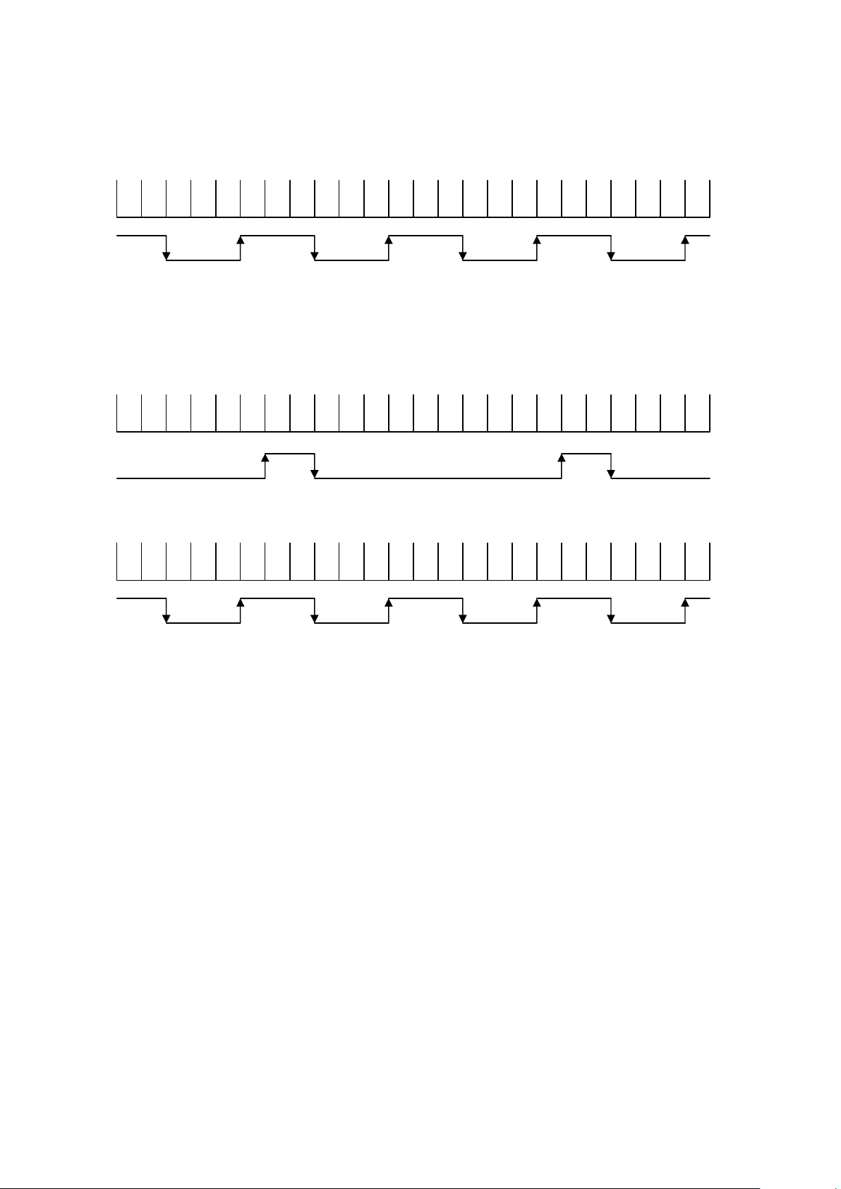
B7~3:VSMP[4:0] : to set the rising edge position of image sampling for AFE.
B2~0:VSMPW[2:0] : to set the pulse width of image sampling.
(1). Color,fine gray or fine line-art : 12 phase/pixel
5 6 7 8 9 10 11 0 1 2 3 4 5 6 7 8 9 10 11 0 1 2 3 4
AFE VSMP
Reg58=52H : VSMP[4:0]=10H VSMPW[2:0]=2H
Page 38
GL841 USB 2.0 2-i n -1 Scanner Contr ol ler
Version 1.6
38
(2).Fast gray or fast line-art : 6 phase/pixel
0 1 2 3 4 5 0 1 2 3 4 5 0 1 2 3 4 5 0 1 2 3 4 5
VSMP
Reg58=0BH : VSMP[4:0]=01H VSMPW=3H
61. Reg : 59H (Read/Write)
Default : 00H
B7~3:BSMP[4:0] : to set the rising edge position of dark voltage sampling for AFE.
B2~0:BSMPW[2: 0] : to set the pulse wi dth of dark voltage sampling.
(1). Color,fine gray or fine line-art: 12 phase/pixel
5 6 7 8 9 10 11 0 1 2 3 4 5 6 7 8 9 10 11 0 1 2 3 4
AFE BSMP
Reg59=52H : BSMP[4:0]=10H BSMPW[2:0]=2H
(2).Fast gray or fast line-art : 6 phase/pixel
0 1 2 3 4 5 0 1 2 3 4 5 0 1 2 3 4 5 0 1 2 3 4 5
BSMP
Reg59=0BH : BSMP[4:0]=01H BSMPW=3H
62. Reg : 5AH (Read/Write)
Default : C0H
B7 : ADCLKINV : set: ADC clock reverse.
B6 : RLCSEL : set: select reset level clamp on a pixel-by-pixel basis.
: reset: don’t select.
B5~4 :CDSREF[1:0] : to set the front-end CDSREF for line rate scanning type.
B3~0 :RLC[3:0] : to set the front-end RLC for line rate scanning type.
63. Reg : 5BH,5CH (Read/Write)
Default : 00H,00H
GMMADDR[9:0]: to set gamma access start address.
64. Reg : 5DH (Read/Write)
Default : 00H
HISPD[7:0] : to set change of the moving spe ed during moving.
Note: can not be programmed to logic zero.
65. Reg : 5EH (Read/Write)
Default : 00H
B7~5:DECSEL[2:0] :select deceleration steps whenever go home.
000:1 steps deceleration
001:2 steps deceleration
010:4 steps deceleration
011:8 steps deceleration
Page 39
GL841 USB 2.0 2-i n -1 Scanner Contr ol ler
Version 1.6
39
100:16 steps deceleration
101:32 steps deceleration
110:64 steps deceleration
111:128 steps deceleration
B4~0:STOPTIM[4:0] :select acceleration/deceleration stop time.
Note: STOPTIM simulation for ASIC must be set to tgtime=6,7.
Can not be programmed to logic zero.
66. Reg : 5FH (Read/Write)
Default : 00H
FMOVDEC[7:0] : to set go-home fa st m o ve deceleration slope steps (table five slope).
Note: can not be programmed to logic zero.
67. Reg : 60H,61H,62H (Read/Write)
Default : 00H,00H,00H
Z1MOD[20:0]: to set the slope curve of acceleration/deceleration table mode value
Under buffer full moving.
Note: It should be more than LPERIOD.
68. Reg : 63H,64H,65H (Read/Write)
Default : 00H,00H,00H
Z2MOD[20:0]: to set the slope curve of acceleration/deceleration mode value
Under first time moving to scanning .
Note: It should be more than LPERIOD.
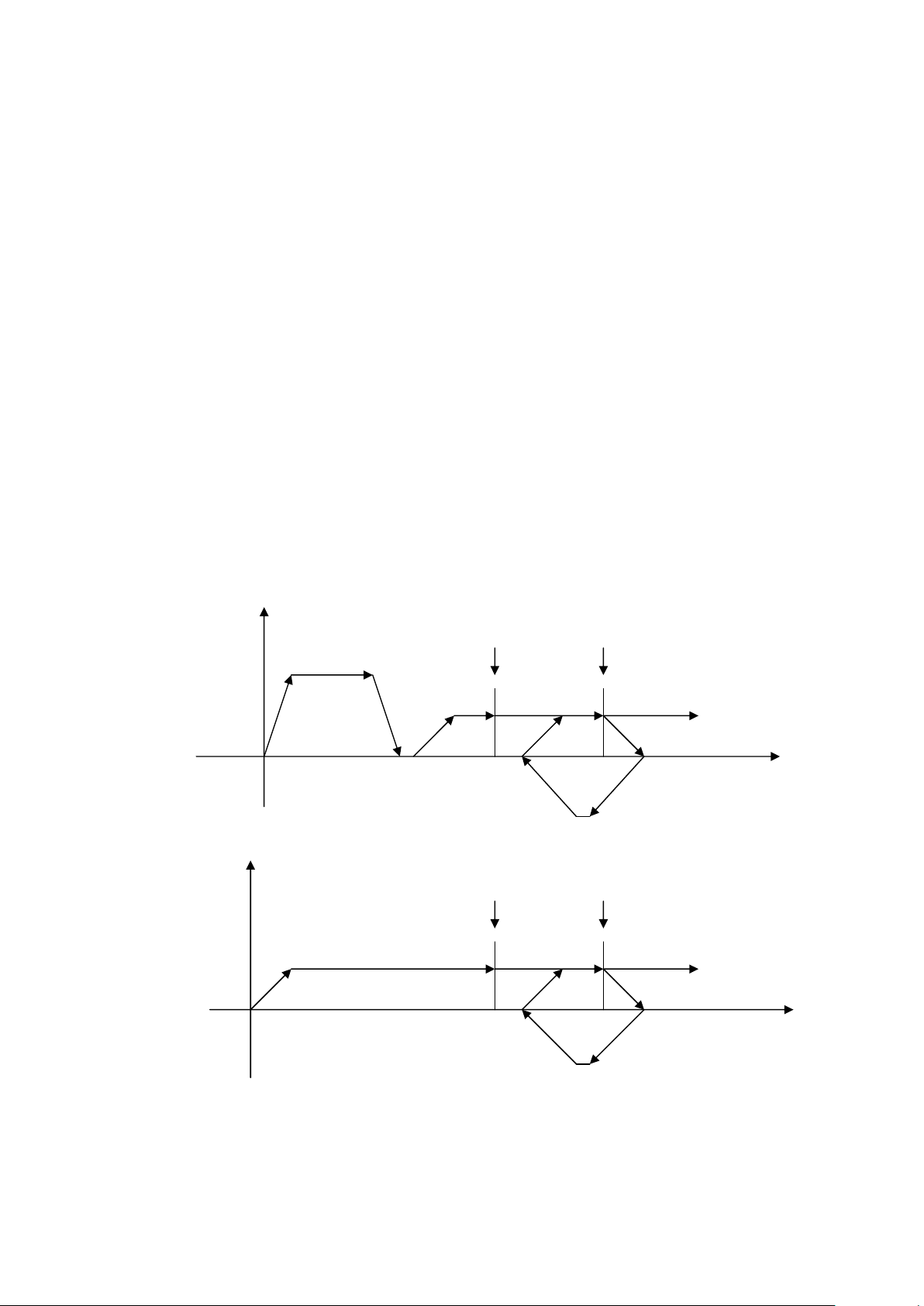
(1). Two table moving :
speed Scanning position buffer full position
b d
a c
time
(2). One table moving :
speed
Scanning position buffer full po s ition
b d
a c
time
{a+(b-1)} mode LPERIOD = Z2MOD
{c+(d-1)} mode LPERIOD = Z1MOD
note: If MCNTSET[1:0]=01 or 10 or 11,then (each step curve value + 1)/VCNT.
Page 40

GL841 USB 2.0 2-i n -1 Scanner Contr ol ler
Version 1.6
40
VCNT= system clocks per pixel / (MCNTSET+1).
69. Reg : 66H (Read/Write)
Default : 00H
PHFREQ[7:0]: to set PWM frequency for motor phase of uni-polar.
Frequency : (24MHz)/[(PHFREQ+1)*4
70. Reg :67H (Read/Write)
Default : 7FH
B7~6:STEPSEL[1:0] : for table one or two scanning move step type selection.
(1).bi-polar :
a.00: full step (for 1939,1940,2916,6219 or 3966).
b.01: half step (for 1939,19 40,2916,6219 or 39 66).
c.10: quarter step (for 2916 or 6219).
d.11: reserved.
(2).uni-polar :
a.00: two-phase-on full step.
b.01: half step.
c.10: reserved.
d.11: single-phase-on full step.
B5~0:MTRPWM[5:0] : to set PWM duty cycle for table one motor phase of uni-polar.
MTRPWM = 0 1/64 duty
= 1 2/64 duty
= 2 3/64 duty
……
= 63 64/64 duty
Note: If PHFREQ < 0FH,then PWM setting must < (PHFREQ+1)*4
71. Reg :68H (Read/Write)
Default : 7FH
FSTPSEL[1:0] : for table two fast moving step type selection.
(1).bi-polar :
a.00: full step (for 1939,1940,2916,6219 or 3966).
b.01: half step (for 1939,1940,2916,6219 or 3966).
c.10: quarter step (for 2916 or 6219).
d.11: reserved.
(2).uni-polar :
a.00: two-phase-on full step.
b.01: half step.
c.10: reserved.
d.11: single-phase-on full step.
FASTPWM[5:0] : to set PWM duty cycle for table two motor phase of uni-polar.
FASTPWM =0 1/64 duty
=1 2/64 duty
=2 3/64 duty
……
=63 64/64 duty
Note: If PHFREQ < 0FH,then PWM setting must < (PHFREQ+1)*4
72. Reg :69H (Read/Write)
Default : 00H
FSHDEC[7:0]: Set scan-finish deceleration slop steps(table three slope).
Note: can not be programmed to logic zero.
73. Reg :6AH (Read/Write)
Default : 00H
Page 41
GL841 USB 2.0 2-i n -1 Scanner Contr ol ler
Version 1.6
41
FMOVNO[7:0]: Set fast moving slop steps(table four slope).
Note: can not be programmed to logic zero.
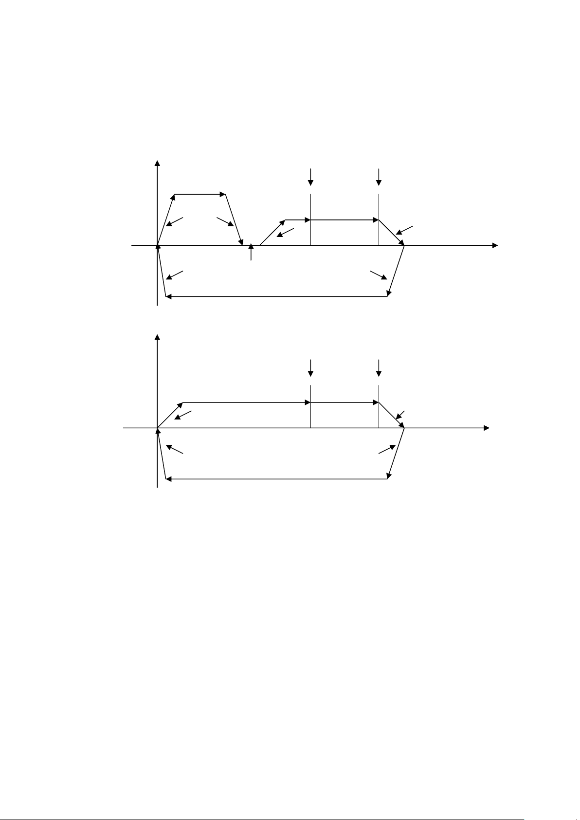
(1). Two table moving :
speed Scanning position scan finished
Reg3D,3E,3F
Reg6A Reg1F Reg25,26,27
Reg21 Reg69
Reg5E[7:5] Reg5E[4:0] Reg6A time
Reg5F
Go home
(2). One table moving :
speed
Scanning position scan finished
Reg3D,3E,3F Reg25,26,27
Reg21 Reg69
time
Reg5F
Reg5E[7:5] Reg6A
Go home
74. Reg :6BH (Read/Write)
Default : 00H
B7 : MULTFILM : to control motor phase idle to meet multi-film scan.
B6 :GPOM13 : set : output MOTORTGO.
: reset : output GPO13.
B5~4:GPOM12~11 : to select GPIO12~11 as Bi-polar motor driver V-ref input voltage in
order to control drive current.
Note : GPIO12: 1. Pull up by resister to indicate that ASIC turn on lamp power
whenever power on initial.
2. Pull down by resister to indicate that ASIC turn off lamp
power whenever power on initial.
3. This pin can control bi-polar motor driver
1939,1940,2916,6219 or 3955 Vref in order to control
Imax.current.
GPIO11: This pin can control bi-polar motor driver 1939,1940,2916,6219
or 3955 Vref in order to Control Imax. current.
Page 42
GL841 USB 2.0 2-i n -1 Scanner Contr ol ler
Version 1.6
42
B3 : Reserved.
B2 : Reserved.
B1~0:GPO18~17 : output GPO18,GPO17 ports.
75. Reg :6CH,6DH (Read/Write)
Default : 00H,00H
GPIO[16:1] : GPIO16~1 outputs ports
76. Reg :6EH,6FH (Read/Write)
Default : 00H,00H
GPOE[16:1] : GPO16~1 ports output enable set.
Set ‘1’ : output.
Reset ‘0’ : input.
77. Reg : 70H,71H (Read/Write)
Default:15H,17H
RSH[4:0] : set CCD RS rising edge position.
RSL[4:0] : set CCD RS falling edge position.
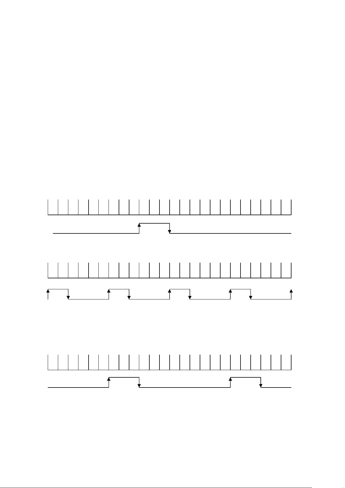
(1). Color,fine gray or fine line-art: 12 phase/pixel
0 1 2 3 4 5 6 7 8 9 10 11 0 1 2 3 4 5 6 7 8 9 10 11
CCD RS : RSH=08H RSL=0BH
(2).Fast gray or fast line-art : 6 phase/pixel
0 1 2 3 4 5 0 1 2 3 4 5 0 1 2 3 4 5 0 1 2 3 4 5
CCD RS : RSH=05H RSL=01H
78. Reg : 72H,73H (Read/Write)
Default:15H,17H
CPH[4:0] : set CCD CP rising edge position.
CPL[4:0] : set CCD CP falling edge position.
(1). Color,fine gray or fine line-art : 12 phase/pixel
5 6 7 8 9 10 11 0 1 2 3 4 5 6 7 8 9 10 11 0 1 2 3 4
CCD CP : CPH=0AH CPL=01H
Page 43
GL841 USB 2.0 2-i n -1 Scanner Contr ol ler
Version 1.6
43
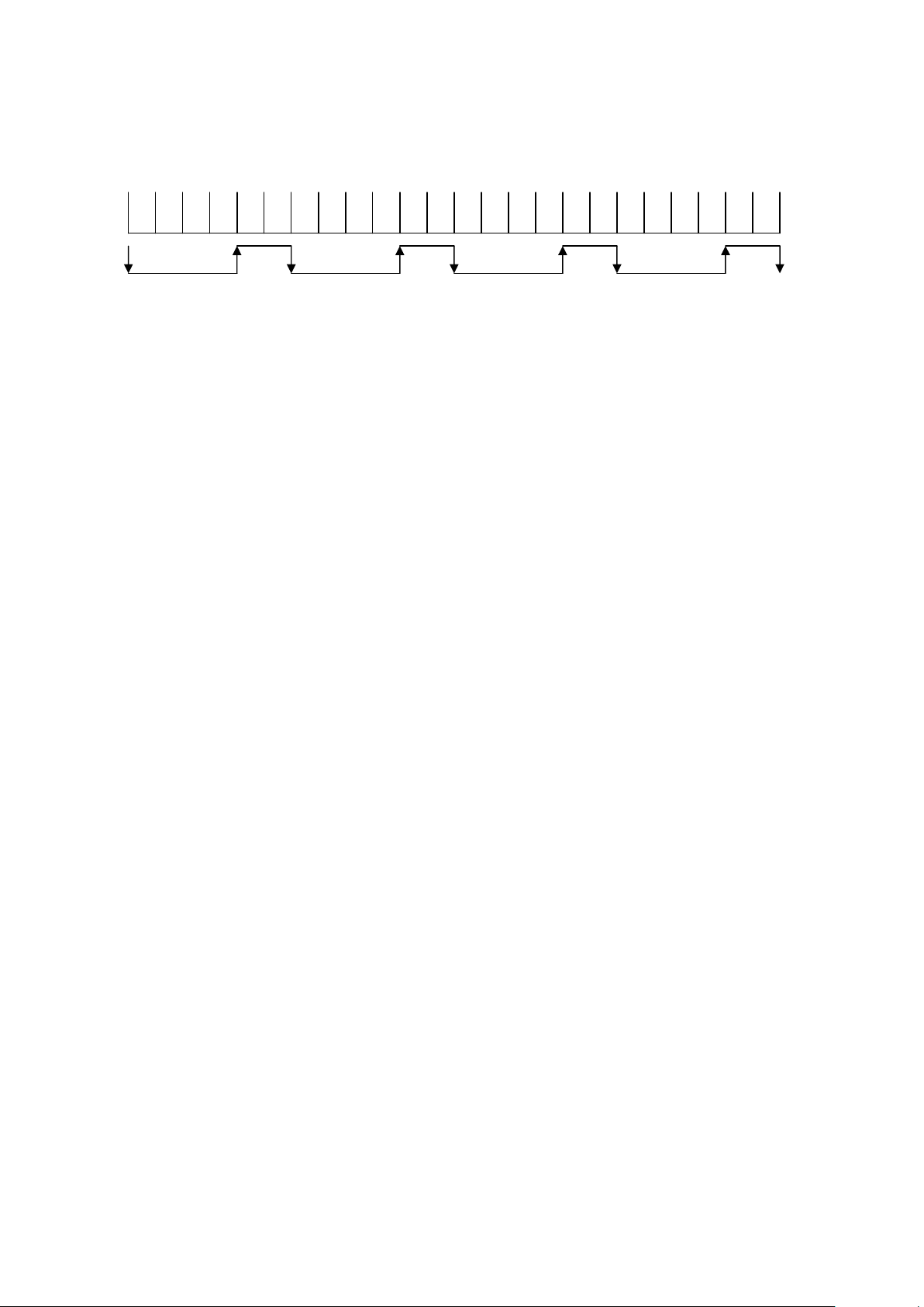
(2).Fast gray or fast line-art : 6 phase/pixel
0 1 2 3 4 5 0 1 2 3 4 5 0 1 2 3 4 5 0 1 2 3 4 5
CCD CP : CPH=03H CPL=05H
79. Reg : 74H,75H,76H (Read/Write)
Default : 00H,00H,00H
CK1MAP[17:0] : CCD clock 1 bit s mapping function.
80. Reg : 77H,78H,79H (Read/Write)
Default : 00H,00H,00H
CK3MAP[17:0] : CCD clock 3 bit s mapping function.
81. Reg : 7AH,7BH,7CH (Read/Write)
Default : 00H,00H,00H
CK4MAP[17:0] : CCD clock 4 bit s mapping function.
82. Reg : 7DH (Read/Write)
Default : 00H
B7: CK1NEG : set: CCD clock1,clock2 output locate at negative edge position of system clock.
: reset : CCD clock1,clock2 output locate at positive edge position of system clock.
B6: CK3NEG : set : CCD clock3 output locate at negative edge position of system clock.
: reset : CCD clock3 output locate at positive edge position of system clock.
B5: CK4NEG : set : CCD clock4 output locate at negative edge position of system clock.
: reset : CCD clock4 output locate at positive edge position of system clock.
B4: RSNEG : set : CCD RS output locate at negative edge position of system clock.
: reset : CCD RS output locate at positive edge position of system clock.
B3: CPNEG : to set CCD CP output locate at negative edge position of system clock.
: reset : CCD CP output locate at positive edge position of system clock.
B2: BSMPNEG : set : AFE video sample output locate at negative edge position of system clock.
: reset : AFE video sample output locate at positive edge position of system clock.
B1: VSMPNEG : set : AFE dark sample output locate at negative edge position of system clock.
: reset : AFE dark sample output locate at positive edge position of system clock.
B0: DLYSET : set : to enable VSMP and BSMP to delay output by 8.33ns unit
: reset : disable this function.
83. Reg : 7EH (Read/Write)
Default : 00H
B5 :GPOLED18 : set : GPIO 18 as LED outout.
: reset : GPIO18 as general I/O.
B4 :GPOLED17 : set : GPIO 17 as LED outout.
: reset : GPIO17 as general I/O.
B3 :GPOLED16 : set : GPIO 16 as LED outout.
: reset : GPIO16 as general I/O.
B2 :GPOLED15 : set : GPIO 15 as LED outout.
: reset : GPIO15 as general I/O.
B1 :GPOLED14 : set : GPIO 14 as LED outout.
: reset : GPIO14 as general I/O.
B0 :GPOLED13 : set : GPIO 13 as LED outout.
: reset : GPIO13 as general I/O.
Page 44

GL841 USB 2.0 2-i n -1 Scanner Contr ol ler
Version 1.6
44
84. Reg : 7FH (Read/Write)
Default : 00H
B7~6 :[1:0]BSMPDLY : to set BSMP output delay.
2’b00: no delay.
2’b01:delay 8.33ns
2’b10:delay 16.67ns
2’b11:delay 25ns.
B5~4 :[1:0]VSMPDLY : to set VSMP output delay.
2’b00: no delay.
2’b01:delay 8.33ns
2’b10:delay 16.67ns
2’b11:delay 25ns.
B3~0 :[3:0]LEDCNT : to set LED blinking speed.
The unit is 100ms.
85. Reg : 80H (Read/Write)
Default:00H
B7~6: VRHOME[1:0] : to set the Vref. of the motor driver IC for go-home moving.
B5~4: VRMOVE[1:0] : to set the Vref. of the motor driver IC for fast forward moving.
B3~2: VRBACK[1:0] : to set the Vref. of the motor driver IC for backward moving.
B1~0: VRSCAN[1:0] : to set the Vref. of the motor driver IC for scan forward moving.
86. Reg : 81H,82H (Read/Write)
Default:00H,00H
B8~0: ROFFSET[8:0] : to set R Channel Offset of the AFE for CIS color scan.
87. Reg : 83H,84H (Read/Write)
Default:00H,00H
B8~0: GOFFSET[8:0] : to set G Channel Offset of the AFE for CIS color scan.
88. Reg : 85H,86H (Read/Write)
Default:00H,00H
B8~0: BOFFSET[8:0] : to set B Channel Offset of the AFE for CIS color scan.
89. Reg : 87H (Read/Write)
Default:00H
B7 : Reserved.
B6 : YENB : set: to enable PH_Y output of the YBIT.
: reset: to disable PH_Y output of the YBIT.
B5 : YBIT : to output PH_Y status.
B4 : ACYCNRLC : set: to generate RLC/ACYC pulse to trigger WM8199 auto-cycling for
Line-by-line color scanning.
: reset: to disable this function.
B3 : ENOFFSET : set: to select automatic offset configuration for CIS scanning.
: reset: to disable this function.
B2 : LEDADD : set: enable true gray by controlling CIS RGB LED array.
: reset: normal gray by controlling CIS single color LED array.
B1 : CK4ADC : set: to select ADCCLK output by CK4MAP setting.
: reset: to select ADCCLK output by default.
B0 : AUTOCONF : set: to enable automatic channel,offset configuration or or RLC/ACYC pulsing
for CIS color scan.
: reset: to disable these function.
Note: If YBIT=1,then YENB=1 PH_Y=1;YENB=0 PH_Y=0.
If YBIT=0,then YENB=1 PH_Y=0;YENB=0 PH_Y=1.
Page 45
GL841 USB 2.0 2-i n -1 Scanner Contr ol ler
Version 1.6
45
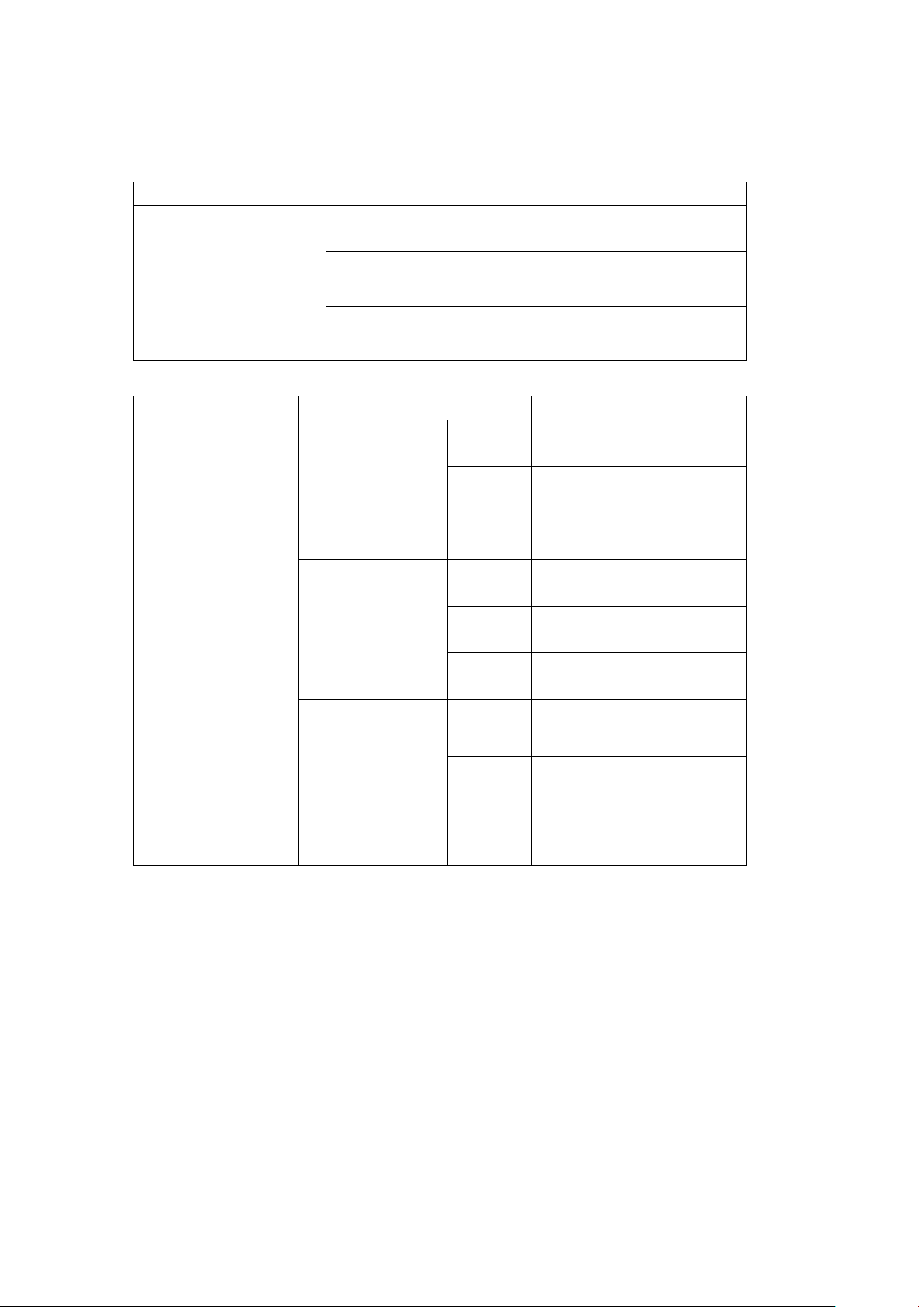
90. Shading mapping(Chunky for single bank)
Attribute Resolution
Address[19:0]
600dpi
(DPIHW=00)
00000H~07FFFH
SIZE : 32k
1200dpi
(DPIHW=01)
00000H~0FFFFH
SIZE : 64k
Shading Mapping
2400dpi
(DPIHW=10)
00000H~1FFFFH
SIZE : 128k
91. Shading mapping(Planer)
Attribute Resolution
Address[19:0]
RED
CHANNEL
00000H~029FFH
GREEN
CHANNEL
02A00H~053FFH
600dpi
(DPIHW=00)
BLUE
CHANNEL
05400H~07DFFH
RED
CHANNEL
00000H~054FFH
GREEN
CHANNEL
05500H~0A9FFH
1200dpi
(DPIHW=01)
BLUE
CHANNEL
0AA00H~0FEFFH
RED
CHANNEL
00000H~0A7FFH
GREEN
CHANNEL
0A800H~14FFFH
Shading Mapping
2400dpi
(DPIHW=10)
BLUE
CHANNEL
15000H~1F7FFH
Page 46
GL841 USB 2.0 2-i n -1 Scanner Contr ol ler
Version 1.6
46
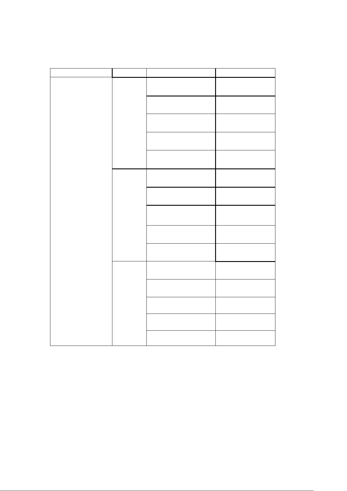
92. Slope Curve Table Mapping :
Attribute Resolution Table no.
Address[19:0]
TABLE 1 08000 ~ 081FF
TABLE 2
08200 ~ 083FF
TABLE 3 08400 ~ 085FF
TABLE 4 08600 ~ 087FF
600DPI
(DPIHW=00)
TABLE 5 08800 ~ 089FF
TABLE 1
10000 ~ 101FF
TABLE 2
10200 ~ 103FF
TABLE 3
10400 ~ 105FF
TABLE 4
10600 ~ 107FF
1200DPI
(DPIHW=01)
TABLE 5
10800 ~ 109FF
TABLE 1
20000 ~ 101FF
TABLE 2 20200 ~ 203FF
TABLE 3 20400 ~205FF
TABLE 4 20600 ~207FF
Slope Curve Table
2400DPI
(DPIDW=10)
TABLE 5 20800 ~209FF
Page 47
GL841 USB 2.0 2-i n -1 Scanner Contr ol ler
Version 1.6
47
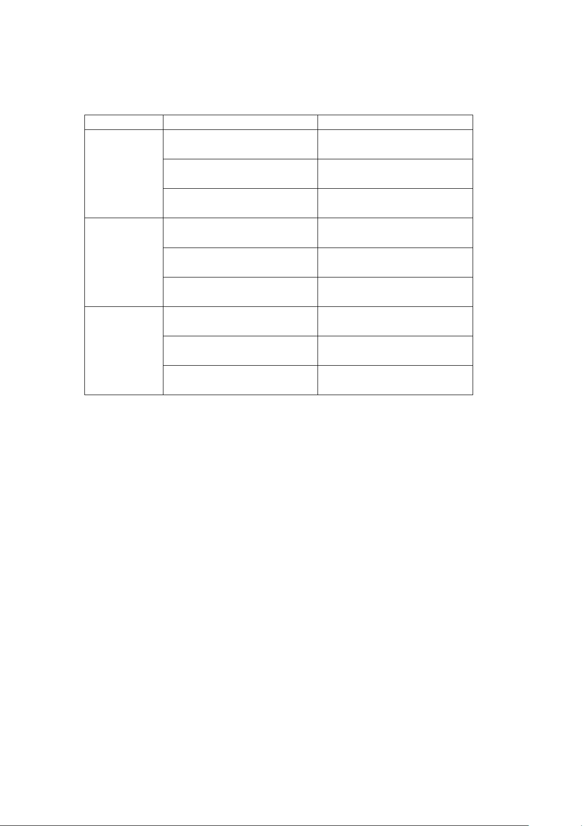
93. Image Buffer Mapping :
DRAM SIZE Resolution
Address[19:0]
600DPI
(DPIHW=00)
09000H~3FFFFH
1200DPI
(DPIHW=01)
11000H~3FFFFH
DRAM/SRAM
4M BITS X 1
2400DPI
(DPIHW=10)
21000H~3FFFFH
600DPI
(DPIHW=00)
09000H~7FFFFH
1200DPI
(DPIHW=01)
11000H~7FFFFH
DRAM
4M BITS X 2
or
8M BITS
SRAM
2400DPI
(DPIHW=10)
21000H~7FFFFH
600DPI
(DPIHW=00)
09000H~FFFFFH
1200DPI
(DPIHW=01)
11000H~FFFFFH
DRAM
16M BITS
2400DPI
(DPIHW=10)
21000H~FFFFFH
Page 48
GL841 USB 2.0 2-i n -1 Scanner Contr ol ler
Version 1.6
48
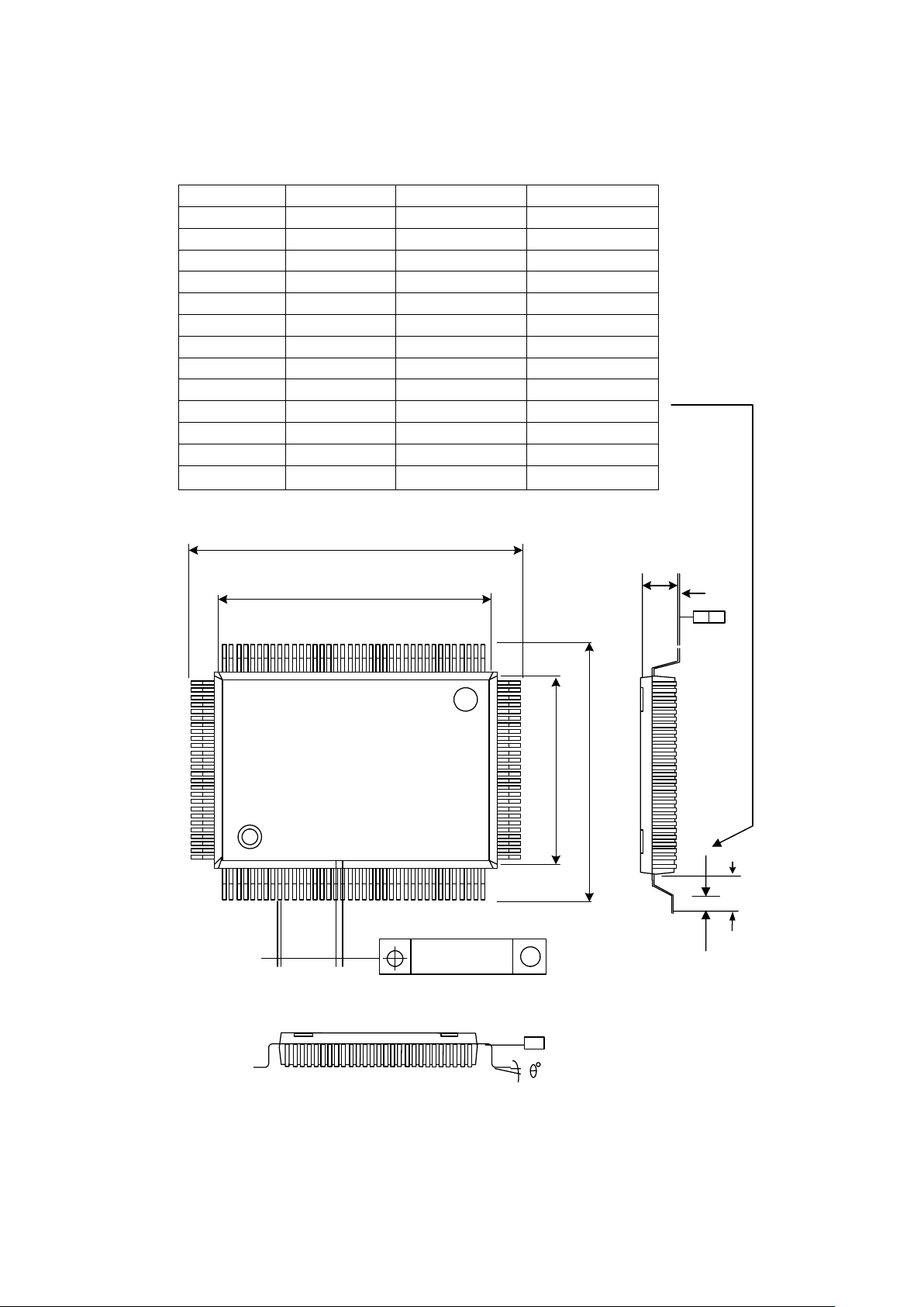
8 Package – 128QFP :
SYMBOLS MIN(mm) NOM(mm) MAX(mm)
A1 0.25 0.35 0.45
A2 2.57 2.72 2.87
b 0.10 0.20 0.30
C 0.10 0.15 0.20
D 13.90 14.00 14.10
E 19.90 20.00 20.10
e - 0.50 Hd 17.00 17.20 17.40
He 23.00 23.20 23.40
L 0.65 0.80 0.95
L1 - 1.60 Y - - 0.08
Θ
0 - 12
9
e
b
0.08(0.003)
M
E
He
D
Hd
L1
A2
A1
Y
H
D
 Loading...