

Page 1
GL6840
GL6840A
Electronic Two Tone Ringer
Description
GL6840A are monolithic integrated circuits designed
to replace the mechanical bell in telephone sets,
in connection with an electro acoustical converter.
The device can drive either directly a piezo ceramic
converter(buzzer) or a small loudspeaker. In this
case a transformer is needed. The two tone frequencies generated are switched by an internal oscillator
in a fast sequence and made audible across output
amplifiers in the transducer, both tone frequencies
and switching frequency can be externally adjusted.
The supply voltage is obtained from the AC rings
signal and the circuit is designed so that noise on the
line or variations on the ringing signal cannot affect
the correct operation of the devices.
The output bridge configuration allows to use a high
impedance transducer with acoustical results much
better than in a single ended configuration. The two
outputs can also be connected independently to
different converters or actuators(acoustical, opto and
logic)
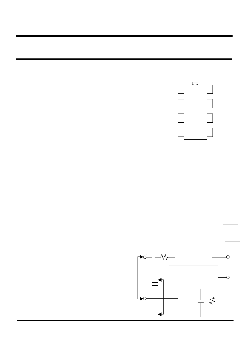
Pin Configuration
Line 1
GND
Sweep rate
control capacitor
Output freq.
Control resistor
2
3
4
8
7
6
GL6840A
5
(Top View)
Absolute Maximum Ratings
Calling Voltage(f=50§Ô)
continuous
Calling Voltage(f=50§Ô)
5s ON/10s OFF
Supply Current
Operating Temperature
Storage Temperature
Line
Rectifier
capacitor
Buzzer
Buzzer
120Vrms
200Vrms
22§Ì
-20 to 75¡É
-65 to 150¡É
Features
• Low current consumption, in order to allow the
parallel operation of 4 devices
• Integrated rectifier bridge with zener diodes to
protect against overvoltages
• Little external circuitry
• Tone and switching frequencies adjustable by
external components
• Integrated voltage and current hysteresis
• Bridge output configuration
1
Test Circuit
For GL6840A
1§Þ 2.2§Ú
VAB Line
£«
10§Þ
3.26 x 10
R1(§Ú)
f2= 0.717 x f
8 5
GL6840A
7
1 2 3 4
VS
1
C1
100§Ý
4
x (2 - e )f1=
f
sweep
=
6
R1
14§Ú
14 - R1(§Ú)
95
1000
C1(§Ý)
Buzzer
Page 2
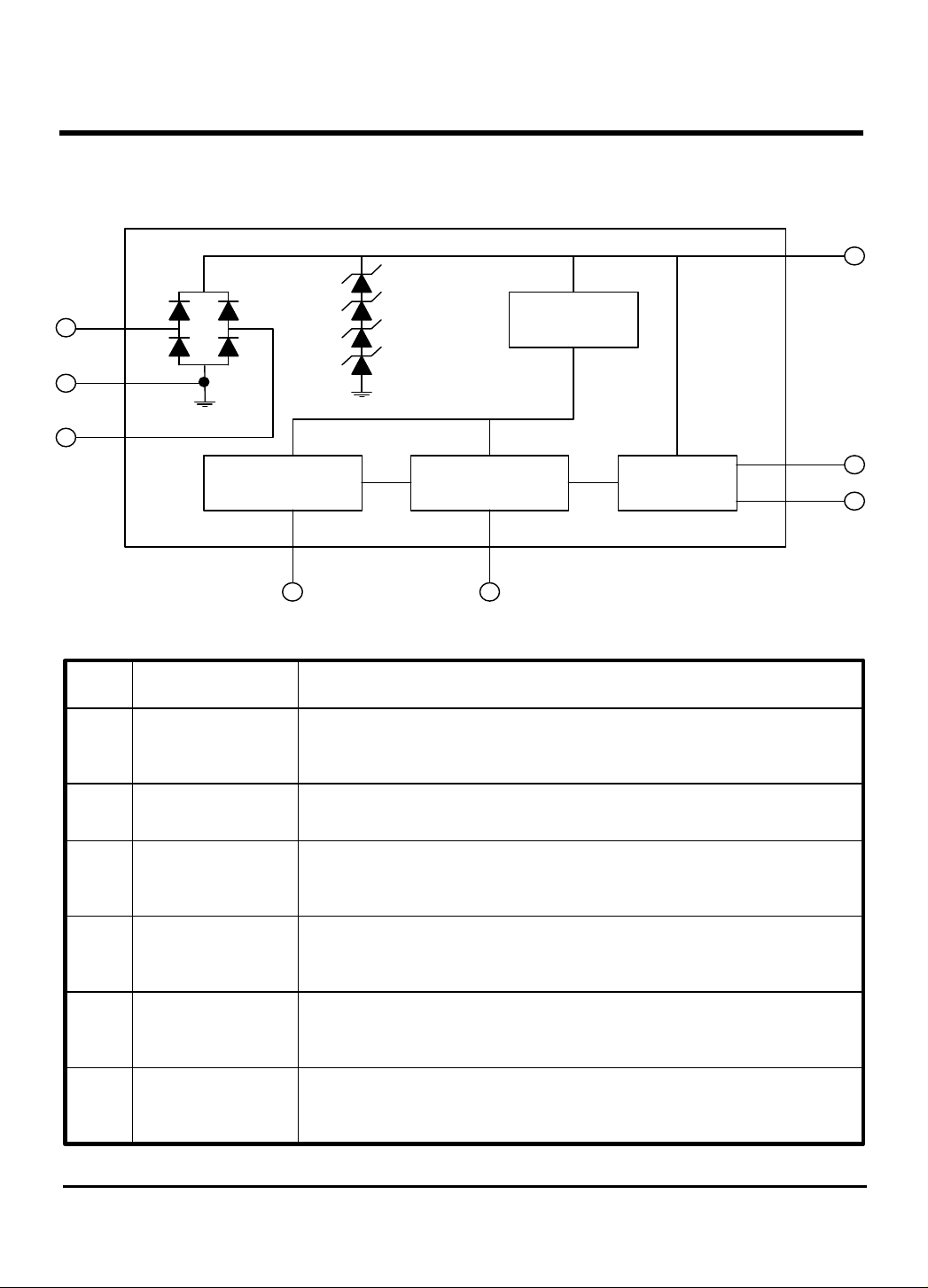
Block Diagram
8
2
1
Sweep Frequency
Bridge
Diode
Oscillator
3 4
Overvoltage
Protection
Tone Generation
Oscillator
Threshold
Detector
Output
Stage
GL6840
7
5
6
Pin Description
PIN NAME DESCRIPTION
1,8 LINE
2 GND
3
4
5,6 Buzzer
7
Sweep Rate
Control Capacitor
Output Frequency
Control Resistor
Rectifier
Capacitor
Input terminals to bridge diode. The AC ringing signal from the
telephone line drives the ringer through bridge.
Ground
This pin is connected to external capacitor to control the sweeping
frequency(fSWEEP)
This pin is connected to external resistor to control the two tone
frequency(f1, f2)
The tone ringer output terminals which have inverse output phase
each others.
This pin is connected to external capacitor to change AC ringing
signal into DC voltage.
2
Page 3

Electrical Characteristics : TA=25¡Éunless otherwise specified
GL6840
PARAMETER
Supply Voltage
Current Consumption without
load(pin 1-8)
Activation Voltage VON 14.4 V
Sustaining Voltage VOFF 9.7 V
Differential Resistance in
OFF condition(pin 8-1)
SYMBOL
CONDITIONS MIN. TYP. MAX.26UNIT
VS(pin7)
IB VS=16.5 to 29.5V 1.2 1.8
13.3
8.9
RD
12.3
8
6.4
§Ì
§Ú
Output Voltage Swing VOUT VVS-5
Short Circuit Current
(pin 5-6)
Voltage Drop between
pin 8-1 and pin 7-2
Output Frequencies
FOUT1
FOUT2
IOUT VS=20V 35
VD 3 V
VS=26V R1=14§Ú
F1
F2
VS=0V
VS=6V
1.96
1.42
2.3
1.67
2.65
1.92
§Ì
§Õ
V
Programming Resistor Range
Sweep Frequency
8 20
7 13FSWEEP C1=100§Ý 10
3
§Ú
§Ô
Page 4

Typical Application
Figure1 : Single output applied pin#5
GL6840
TIP
VAB Tel Line
RING
1§Þ 250V AC 2.2§Ú
C2 R2
£«
C3
10§Þ
VS
8 5
7
1 2 3 4
Figure2 : Single output applied pin#6
TIP
VAB Tel Line
RING
1§Þ 250V AC 2.2§Ú
C2 R2
£«
C3
10§Þ
VS
8 5
7
1 2 3 4
6
GL6840A
C1
100§Ý
6
GL6840A
C1
100§Ý
R1
14§Ú
R1
14§Ú
10§Ú
10§Ú
VoutPiezo
VoutPiezo
0.22§Þ
10§Ú
0.22§Þ
10§Ú
C
C
C
C
C
C
C
C
Speaker
1300:8§Ù
C
C
C
C
C
C
C
C
Speaker
1300:8§Ù
Note) Using a big size buzzer, pin#6 output is better than pin#5 output.
Figure3 : Differential output
TIP
VAB Tel Line
RING
1§Þ 250V AC 2.2§Ú
C2 R2
£«
C3
10§Þ
VS
8 6
7
1 2 3 4
GL6840A
C1
100§Ý
4
10§Ú
5
R1
14§Ú
0.22§Þ
10§Ú
Piezo
C
C
C
C
C
C
C
C
Speaker
1300:8§Ù
Page 5

GL6840
GL6840B
Electronic Two Tone Ringer
Description
GL6840B are monolithic integrated circuits designed
to replace the mechanical bell in telephone sets,
in connection with an electro acoustical converter.
The device can drive either directly a piezo ceramic
converter(buzzer) or a small loudspeaker. In this
case a transformer is needed. The two tone frequencies generated are switched by an internal oscillator
in a fast sequence and made audible across output
amplifiers in the transducer, both tone frequencies
and switching frequency can be externally adjusted.
The supply voltage is obtained from the AC rings
signal and the circuit is designed so that noise on the
line or variations on the ringing signal cannot affect
the correct operation of the devices.
The output bridge configuration allows to use a high
impedance transducer with acoustical results much
better than in a single ended configuration. The two
outputs can also be connected independently to
different converters or actuators(acoustical, opto and
logic)
Pin Configuration
Line 1
GND
Sweep rate
control capacitor
Output freq.
Control resistor
2
3
4
8
7
6
GL6840B
5
(Top View)
Absolute Maximum Ratings
Calling Voltage(f=50§Ô)
continuous
Calling Voltage(f=50§Ô)
5s ON/10s OFF
Supply Current
Operating Temperature
Storage Temperature
-20 to 75¡É
-65 to 150¡É
Line
Rectifier
capacitor
Buzzer
Buzzer
120Vrms
200Vrms
22§Ì
Features
• Low current consumption, in order to allow the
parallel operation of 4 devices
• Integrated rectifier bridge with zener diodes to
protect against overvoltages
• Little external circuitry
• Tone and switching frequencies adjustable by
external components
• Integrated voltage and current hysteresis
• Bridge output configuration
5
Test Circuit
For GL6840B
1§Þ 2.2§Ú
Line
VAB
£«
10§Þ
3.32 x 10
R1(§Ú)
f2= 0.717 x f
8
GL6840B
7
1 2 3 4
VS
1
C1
100§Ý
4
x (2 - e )f1=
f
sweep
5
=
6
R1
39§Ú
39 - R1(§Ú)
358
1000
C1(§Ý)
Buzzer
Page 6

Block Diagram
8
2
1
Pin Description
Bridge
Diode
Sweep Frequency
Oscillator
3 4
Overvoltage
Protection
Tone Generation
Oscillator
Threshold
Detector
Output
Stage
GL6840
7
5
6
PIN NAME DESCRIPTION
1,8 LINE
2 GND
3
4
5,6 Buzzer
7
Sweep Rate
Control Capacitor
Output Frequency
Control Resistor
Rectifier
Capacitor
Input terminals to bridge diode. The AC ringing signal from the
telephone line drives the ringer through bridge.
Ground
This pin is connected to external capacitor to control the sweeping
frequency(fSWEEP)
This pin is connected to external resistor to control the two tone
frequency(f1, f2)
The tone ringer output terminals which have inverse output phase
each others.
This pin is connected to external capacitor to change AC ringing
signal into DC voltage.
6
Page 7

Electrical Characteristics : TA=25¡Éunless otherwise specified
GL6840
PARAMETER
Supply Voltage
Current Consumption without
load(pin 1-8)
Activation Voltage VON 14.4 V
Sustaining Voltage VOFF 9.7 V
Differential Resistance in
OFF condition(pin 8-1)
SYMBOL
CONDITIONS MIN. TYP. MAX.26UNIT
VS(pin7)
IB VS=16.5 to 29.5V 1.2 1.8
13.3
8.9
RD
12.3
8
6.4
§Ì
§Ú
Output Voltage Swing VOUT VVS-5
Short Circuit Current
(pin 5-6)
Voltage Drop between
pin 8-1 and pin 7-2
Output Frequencies
FOUT1
FOUT2
IOUT VS=20V 35
VD 3 V
VS=26V R1=39§Ú
F1
F2
VS=0V
VS=6V
723
519
850
610
978
702
§Ì
§Ô
V
Programming Resistor Range
Sweep Frequency
27 51
7 13FSWEEP C1=100§Ý 10
7
§Ú
§Ô
7
Page 8

Typical Application
Figure1 : Single output applied pin#5
GL6840
TIP
VAB Tel Line
RING
1§Þ 250V AC 2.2§Ú 0.22§Þ
C2 R2
8 5
7
1 2 3 4
VS
C3
10§Þ
£«
Figure2 : Single output applied pin#6
TIP
VAB Tel Line
RING
1§Þ 250V AC 2.2§Ú
C2 R2
£«
C3
10§Þ
VS
8
7
1 2 3 4
6
GL6840B
C1
100§Ý
6
GL6840B
C1
100§Ý
39§Ú
5
R1
R1
39§Ú
10§Ú
10§Ú
VoutPiezo
VoutPiezo
10§Ú
0.22§Þ
10§Ú
C
C
C
C
C
C
C
C
Speaker
1300:8§Ù
C
C
C
C
C
C
C
C
Speaker
Note) Using a big size buzzer, pin#6 output is better than pin#5 output.
Figure3 : Differential output
TIP
VAB Tel Line
RING
1§Þ 250V AC 2.2§Ú
C2 R2
£«
C3
10§Þ
VS
8 6
7
1 2 3 4
GL6840B
C1
100§Ý
8
10§Ú
5
R1
39§Ú
0.22§Þ
10§Ú
Piezo
1300:8§Ù
C
C
C
C
C
C
C
C
Speaker
1300:8§Ù
 Loading...