

Page 1
1
V
REF
EXP IN
VCC
EXP RECT
ALC
EXP OUT
COMP OUT
C-ACF
COMP RECT
GND
COMP NF
GL6552
EXP MUTE
COMP MUTE
COMP IN
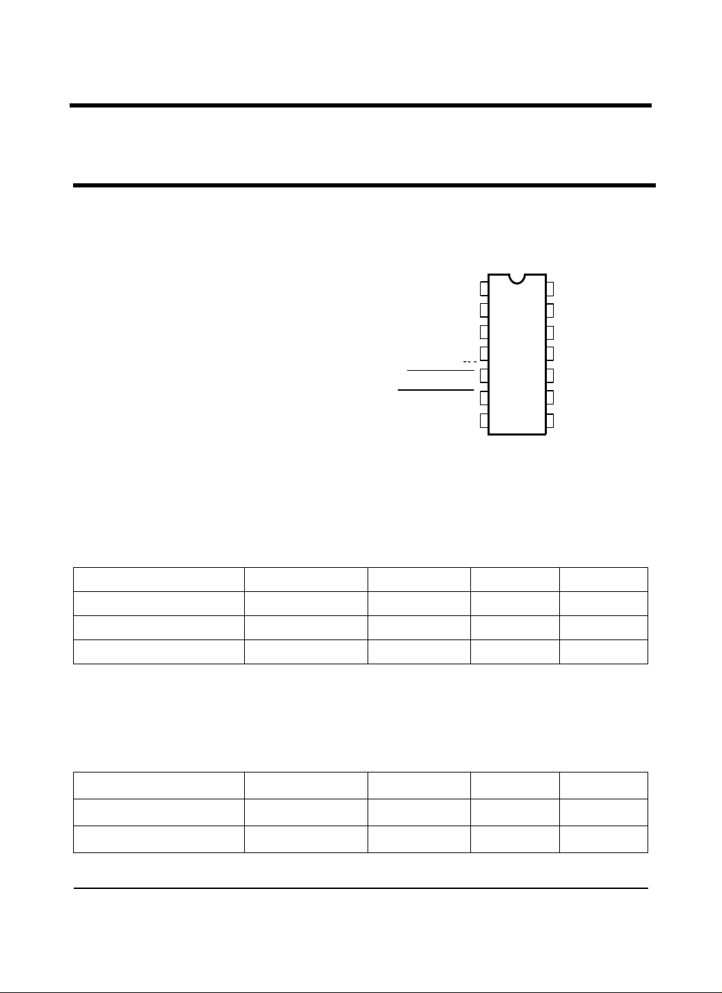
14 DIP, 14 SOP(150mil)
General Descriptions
The GL6552 is a Compander IC, which
contains two variable gain circuits configured
for compressing and expanding the dynamic
range, and improving of S/N ratio of audio
signal. It consists of compressor, expander, Mic
Amp, limiter, ALC(Automatic Level
Control)and mute logic. The compressor circuit
has the 2/1 ratio of input/output ratio by
logarithm, and the expander circuit by
logarithm. An internal, temperature stable
bandgap reference provides the necessary
precision voltage and current. Applications
include cordless telephone and most voice RF
links.
Features
• Operating Supply Voltage: 2 ~ 6 V
• Built in ALC circuit
• Built in Mute logic circuit
• Easy gain control to use external component
Absolute Maximum Ratings(Ta = 25¡É.)
GL6552
GL6552
Low Voltage Compander
Pin Configuration
Parameter Symbol Spec. Unit Remark
Max. Supply Voltage V
Power Dissipation P
Storage Temperature T
Stress above those listed under “Absolute Maximum Rating” may cause permanent damage of device.
This is stress rating only and functional operation of the device at these or any other conditions above
those indicated in the operational sections of this specification is not implied.
Exposure to absolute maximum rating conditions for longer periods may affect device reliability.
During overload conditions (VIN > VCC or VIN <GND), those voltage on VCC pins with respect to ground
must not exceed the values defined by the absolute maximum ratings.
CC, MAX
600 mW
D.MAX
-55 ~+150
STG
7 V
¡É
Operating Conditions (Ta = 25¡É)
Parameter symbol Spec. Unit Remark
Operating Voltage V
Operating Temperature TOP -20 ~ +70
OP
2 ~ 6 V
¡É
Page 2
2
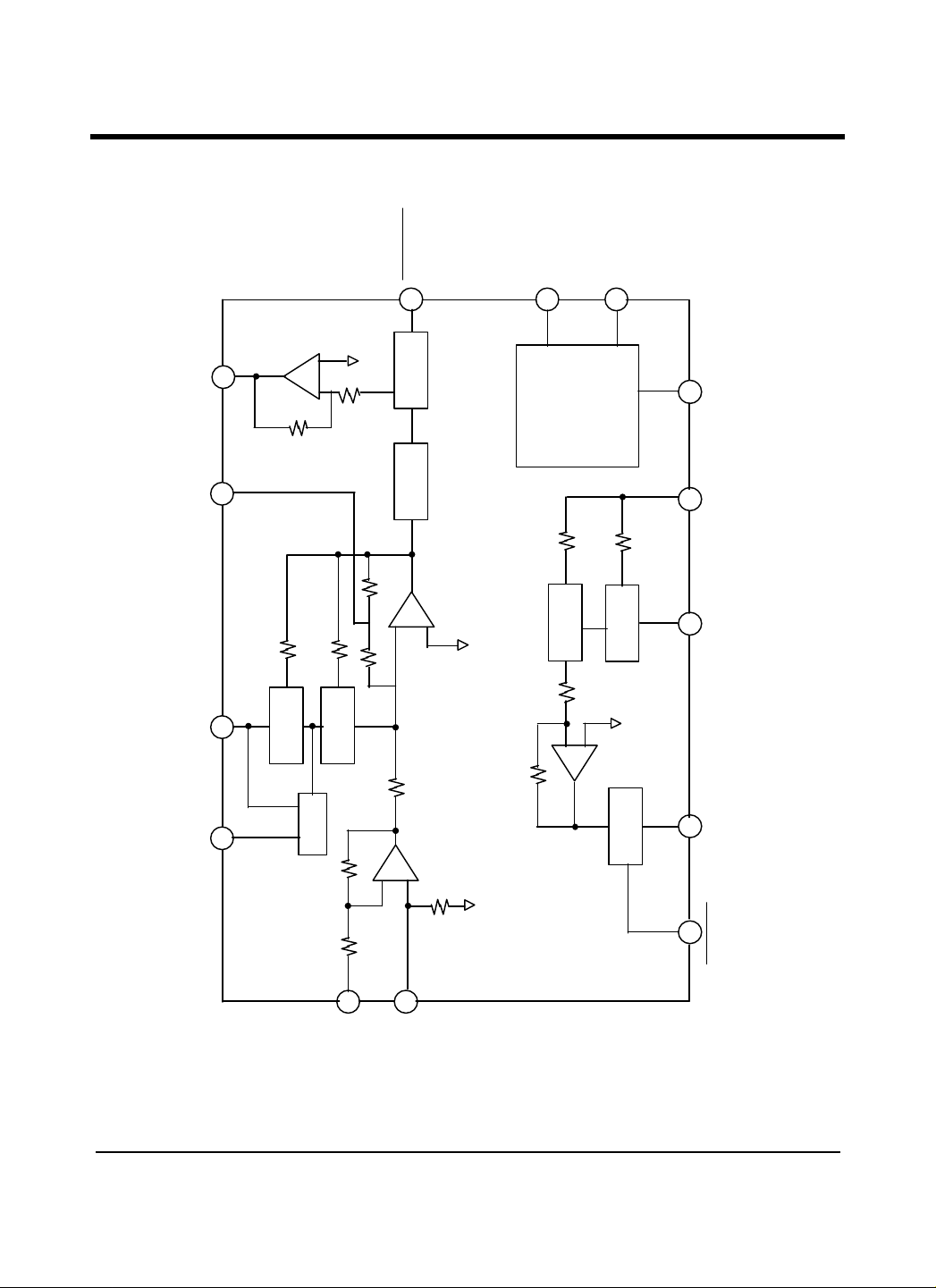
BLOCK DIAGRAM
12
11
10
7
6
14
3 2 5
4 1 9
8
-
-
+
REGULATOR
RECTIFIER
ALC
13
GAIN CELL
MUTE
LIMITER
MUTE
RECTIFIER
GAIN CELL
-
+
COMP OUT
ACF
COMP RECT
ALC
COM P NF
COM P IN
EXP MUTE
EXP OUT
EXP RECT
EXP IN
REF
GND VCC
COMP MUTE
To V
REF
65K 65K 10K 10K
30K
To V
REF
25.8K 3.3K 100K 51K
To V
REF
10K 30K
EXPANDER
COMPRESSOR
GL6552
+
−
C-
+
V
Page 3

3
Pin Description
No.
1 V
2 EXP IN Expander input terminal
3 EXP RECT
4 EXP OUT
5 MUTE EXP
6 MUTECOMP
7 GND Ground terminal
8 COMP IN
Symbol Function
Output terminal of bias circuit (Band Gap of reference). It is an internal
REF
reference voltage used for supplying a constant voltage to the compressor
and the expander.
External rectifing capacitor is connected to this terminal. Attack and decay
time of expander is determined by capacitor.
Expander output terminal
It is an expander mute terminal of a compander.
“L” state – expander mute is executed.
“H” state – expander is executed.
It is an compander mute terminal of a compander.
“L” state – compressor mute is executed.
“H” state – compressor is executed.
Compressor Mic Amp noninverting input terminal. It is used as input
terminal for voice signal.
GL6552
9 COMP NF
10 COMP RECT
11 C-ACF
12 COMP OUT Compressor output terminal.
13 ALC
14 VCC Supply voltage terminal
Compressor Mic Amp inverting input terminal. It is used for determining
Mic Amp gain by resistor
External rectifing capacitor is connected to this terminal. Attack and decay
time of expander is determined by capacitor.
Feedback coupling capacitor is connected to this terminal. Low cut-off
frequency of compressor is determined by this capacitor.
It is a reference voltage input terminal of ALC. ALC circuit may be turned
off according to the ALC reference voltage.
Page 4

GL6552
4
6
1
0
1
-
0
0
-
-
Electrical Characteristics (VCC=3V, f=1KHz, Ta=25¡É unless otherwise specified)
PARAMETER SYMBOL
MIN. TYP. MAX.
DC Electrical Characteristics
Power Supply Current Icc - 3.6
Reference voltage V
0.9
REF
Compressor part
Standard Output Voltage
Gain Difference
VOC 240 300 340 mVrms V
∆Gc1
-1.0
T.H.D THDc - 0.5
Mute Attenuation Ratio ATTc 60 80
Max. Output Voltage V
ALC V
1.15 1.35 1.5 Vp-p V
CMAX
280 325 360 mVrms V
ALCO
Expander part
Standard Output Voltage
Gain Difference
VOE 110 130 160 mVrms V
∆GE1
∆GE1
-0.5
-1.0
T.H.D THDE - 0.5 1.5
Mute Attenuation Ratio ATTE 60 85
Max. Output Voltage V
500 600
EMAX
SPEC.
UNIT
mA No Signal
1.1
V No Signal
1.0 dB V
% V
dB V
0.5 dB V
1.0 dB V
% V
dB V
mVrms V
CONDITION
=13mVrms (=0dB)
INC
= -20dB
INC
=0dB, VCC =-3V
INC
=0dB
INC
=Variable
INC
=0.9V
PIN13
=180mVrms (=0dB)
INE
=-10dB
INE
=-20dB
INE
=0dB
INE
=0dB
INE
=Variable
INE
Page 5

5
Test Circuit
1 2 3 4 5 6 7
14
13
12
11
10
5
9
8
VCC
ALC
COMP OUT
C
ACF
COMP RECT
COMP NF
COMP IN
REF
EXP IN
EXP RECT
EXP OUT
EXP MUTE
COMP
GND
GL6552
AS2
M2
MP6
MP1
MP2
MP3
MP4
MP5
680
10K
3.3§Þ
0.1§Þ
2.2§Þ
1§Þ
1§Þ
K1
K2
K3
K4
K5
K6
K7
K8
K9
SW1
SW2
GL6552
V
-
K20
K19
K18
K17
K16
K15
K14
K13
K12
K11
K10
K21
1§Þ
22§Þ
0.1§Þ
2.2§Þ
0.47§Þ
9.1K
0.015§Þ
680
10K
MP13
MP12
MP11
MP10
MP10
MP9
MP8
AS1
M1
Page 6

6
Application Circuit
12
10
7
6
14
3 2 5 4 1 9 8
-
+
+ −REGULATOR
RECTIFIER
ALC
13
GAIN CELL
MUTE
LIMITER
MUTE
RECTIFIER
GAIN CELL
To V
REF
65K 65K 20K 30K 15K 30K
To V
REF
25.8K 3.3K 100K 51K
To V
REF
10K 15K
30K
11
100
To Tx Modulation
22
+
1
+
0.047
MIC
(from MICOM)
+ 33
§Þ
68nF
68K 220K 6.8K 68nF Form Rx output
6.8K 68K
56k
150 100
To V
REF
§Þ
§Þ
§Þ
GL6552
CUTE
§Þ
§Þ
-
+
§Þ
§Þ
§Þ
 Loading...