

Page 1
1
COMP REF
DATA INC-ACF
COMP NF
COMP IN
GND
1 2 4 3 5
6
7 9 8
18
10
20
19
17
16
15
13
11
12
14
Description
The GL6551 is a compander IC to expand
dynamic range at transmission/reception
systems and to improve the tone quality by
means of restricting noise. Two functions are
loaded on the IC, the one is the compressor
which has the 2/1 ratio of input/output ratio by
logarithm, and the expander which has the 1/w
ratio input/ output ratio by logarithm. The
GL6551equipped with input & filter Amp,
DATA IN OUT terminal. The GL6551 is well
suited for use in cellular radio MCA and handy
telephone set, radio communication systems.
Features
• Low operating supply voltage.
• Equipped with mute function and through function.
• Equipped with compressor MIC Amp and Expander
INPUT Amp
• Equipped with Filter Buffer Amp
• Equipped with DATA IN OUT terminal.
• Operation Voltage (2.4 ~ 7.0V)
• Total gain (10~ 100dB)
Maximum Ratings
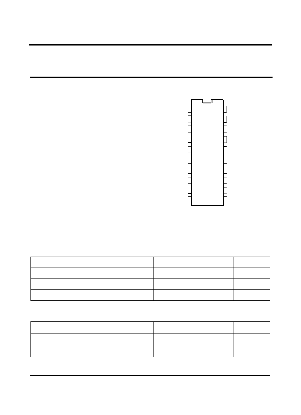
Pin Configuration
FIL OUT
FIL IN
COMP OUT
COMP RECT
GL 6551
GL 6551
COMPANDER
VCC
EXP OUT
EXP RECT
DATA OUT
EXP NF
EXP IN
EXP REF
EXP MUTE
THROUGH
COMP MUTE
Parameter symbol Spec. Unit Remark
Supply Voltage V
Power Dissipation P
Storage Temperature T
CC, MAX
350 mW
D.MAX
-5 ~ 125
STG
10 V
Operating Conditions
Parameter symbol Spec. Unit Remark
Operating Voltage V
OP
Operating Temperature TOP -30 ~ 70
2.4 ~ 7 V
¡É
¡É
Page 2
2
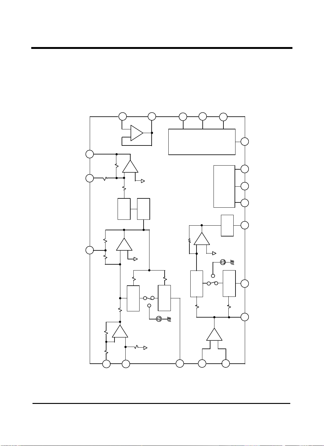
Block Diagram
GND
EXP
MUTE
THROUGH
COMP
MUTE
EXP OUT
EXP RECT
DATA RECT
3 4 5
14
20
1 2 9
12
11
13
17
18
19
10
15
16
6 7 8
−
+
-
+
REGULATOR
S/W CONTROL
MUTE
GAIN CELL
RECTIFIER
GAIN CELL
MUTE
- + -
+
RECTIFIER
-
+
C
DATA IN
COMP IN
FILTER IN
VCC
COMP REF
EXP REF
FILTER OUT
EXP NF
EXP IN
COMP RECT
COMP IN
COMP NF
EXPANDER
COMPRESSOR
100K
100K
100K
3.3K
100K
MIC
INPUTAMP
TH S/W
TH S/W
SUM AMP
SUM AMP
BUFFER AMP
GL 6551
+
−
REF
To V
IDC
30K
-ACF
30K
15K
51K
REF
To V
20K
-AMP
REF
To V
15K
Ith
30K
20K
REF
Ith
To V
10K
Page 3

3
17
0
0
0
-
0
-
0
-
-
-
0
0
0
-
-
-
GL 6551
Electrical Characteristics Ta=25
∗
PARAMETER SYMBOL
MIN TYP MAX
Current Dissipation Icc - 4.0 6.5 mA No Signal
Threshold Voltage Vth 0.9 1.15 1.30
Compressor
Input impedance Zinc 90 120
Input Reference Level Vinc 8 12.5
Gain Deviation (1)
Gain Deviation (2)
Through ON OFF Diff.
∆Gc1
∆Gc2
∆Gtc
-0.5
-1.0
-1.5
T.H.D THDc - 0.5 1.0
Output Noise Voltage Vnc - 3.0 5.5 mVrms
Mute Attenuation Attc 60 80
Limiting Voltage Vlimc 1.15 1.35 1.5 Vp-p
Data Pin Voltage Gain Gdata -0.5
Data Pin Max. Output VDmax 800 900
Cross Talk CTc - -35 -30 dB
Buffer Amp (LPF)
Voltage Gain Gb -0.5
Freq. Charact (1)
Freq. Charact (2)
∆f1
∆f2
- -3
- -60
T.H.D. THDb - 0.02 0.1
Maximum Output Voltage VBmax 550 700
Expander
Output Reference Volt. Voe 110 130 160 mVrms
Gain Deviation (1)
Gain Deviation (2)
Gain Deviation (3)
Through ON OFF Diff.
∆Ge1
∆Ge2
∆Ge3
∆Gte
-0.5
-1.0
-1.5
-2.5 -1 0.5 DB
T.H.D THDe - 0.5 1.5
Output Noise Voltage Vne - 10 30 uVrms
Mute Attenuation VEmax 60 80
Maximum Output Voltage
Gi 700 800
Input Amp Voltage Gain VImax 14.5 15.5 16.5 DB Vin=0dB
Input Amp Max. Voltage
CTe 450 500
Cross Talk - -70 -60 DB
Measured by Noise Filter (CCITT Recommandation P. 53)
SPEC.
¡É,
Vcc=3.0V, f=1kHz, R1=10kΩ
UNIT
CONDITION
V 11, 12, 13 Pin
KΩ
mVrms
0.5 dB
1.0 dB
1.5 dB
Voc=30mVrms,
Vin=0dB
Vin=-20dB ∗
Vin=-40dB ∗
Vin=-0dB, Pin12=0V∗
% Vin=0dB
Rg=620Ω ∗
dB
Vin=0dB, Pin11=0V ∗
0.5 dB Pin4=300mVrms
mVrms THD=10% Point
ExpVin=30mVrms, Rg=620Ω ∗
0.5 dB Vin=300mVrms
dB Vin=300mVrms, f=3kHz
dB Vin=300mVrms, f=30kHz
% Vin=300mVrms
mVrms THD=10% Point
Vin=300mVrms=0dB ∗
0.5 DB
1.0 DB
2.0 DB
Vin=-10dB ∗
Vin=-20dB ∗
Vin=-30dB ∗
Vin=0dB , Pin12=0V ∗
% Vin=0dB
Rg=620Ω ∗
DB
Vin=0dB, Pin13=0V ∗
mVrms THD 10% Point
mVrms THD=10% Point
CompVin=Vinc,Rg=620Ω ∗
∗
Page 4

4
NO
SYMBOL FUNCTION
1 FILTER OUT Filter Amp Output Terminal.
2 FILTER IN
Filter Amp (+) Input Terminal.
Make a various kinds Filters.
3 COMP OUT Compressor Output Terminal.
Connected to (-) Input terminal of Compressor Output Amp
4 DATA IN
through resistor
Signal which is input to this terminal is output to COMP OUT
(Pin3). (not compress)
GL 6551
5 C-ACF
Coupling capacitor connect Terminal.
Determined Low cutoff frequency of Compressor block by capacitance.
Rectifing Capacitor external connect Terminal.
6 COMP RECT
Determined Recovery time and Attack time of Compressor by
Capacitance.
Input resistor and decoupling capacitor of Compressor Mic Amp
7 COMP NF
external connect Terminal. Determined Mic Amp Gain by resistor.
Max gain condition is not connect resistor.
8 COMP IN
Compressor Mic Amp (+) Input Terminal.
Same potential with COMP REF (Pin 9).
9 COMP REF Reference voltage of Compressor Internal Amp Output Terminal.
10
GND Ground Terminal.
“L” state – Compressor Output Mute.
11 COMP MUTE
Input signal of Data In terminal is output to COMP OUT (Pin3).
“H” state – open.
12
THROUGH
“L”state – Compressor and Expander Logalithm 1 (Constant Gain)
“H” state – open.
“L” state = Expander Output is muting.
13
EXP MUTE
Data out to DATA OUT (Pin 17) Terminal.
“H” state – open.
14
EXP REF Reference voltage of Expander Internal Amp output Terminal.
15
16
17
EXP IN Expander Input Amp (+) Input Terminal.
EXP NF Expander Input Amp (-) Input Terminal.
DATA OUT Expander Input Amp Input Terminal.
Rectifing capacitor external connect Terminal.
18
EXP RECT
Determine Attack time and Recovery time of Expander by
Capacitance.
19
20
EXP OUT Expander Output Terminal.
Vcc Power Supply.
Page 5

5
Application Circuit
3
4
5
14
20
1 2 9
12
11
13
17
18
19
10
15
16
6 7 8
REGULATOR
S/W CONTROL
MUTE
GAIN
CELL
RECTIFIER
GAIN CELL
MUTE
-
+
RECTIFIER
-
+
EXPANDER
COMPRESSOR
To V
REF
100K
100K
100K
30K
30K
20K
15K
3.3K
15K
51K
100K
To V
REF
To V
REF
To V
REF
MIC
AMP
INPUT
AMP
TH S/W
TH S/W
SUM
AMP
30K
20K
10K
SUM
AMP
BUFFER A
V
+ 4.7
V
REF
Exp MUTE
+ 4.7
V
REF
THROUGH
COMP
MUTE
Exp OUT
+
1
¥ì
+
2.2
1
¥ì
DATA OUT
1n 10K
10K
6.8n
10
100K
1µ
To VREF
(PIN 9)
Exp IN
2.2
47
Comp IN
100
470n
100n
DATA IN
10K 10K 10K
1n
6.8n + 1
Filter OUT
AMP
+ AMP
GL 6551
¥ì
MP
+
¥ì
IDC
-
CC
C
¥ì
Ith
B
¥ì
Ith
-
¥ì
¥ì
¥ì
 Loading...