

Page 1

Genesys Logic, Inc.
GL652USB
Genesys Logic, Inc.
USB 7 PORT HUB CONTROLLER
DATA SHEET, Version 1.2
Aug. 18, 2000
10F, No.11, Ln.3, Tsao Ti Wei, Shenkeng, Taipei, Taiwan
Tel: 886-2-2664-6655 Fax: 886-2-2664-5757
http://www.genesyslogic.com
Page 2

GL652USB 7 PORT USB HUB CONTROLLER
1 FEATURES
• High performance and low-cost solution for USB hub
• USB Specification Compliance
− Conforms to USB specification Rev. 1.1
− Supports 1 device address and 2 endpoints
• 8-bit micro-processor
− RISC-like architecture
− USB optimized instruction set
− Single cycle instruction execution
− Operation Speed: DC to 24 MHz clock input
− Performance: 12 MIPS @ 24MHz
• I/O ports
− 7-port hub
• Internal memory
− 64 bytes of RAM
− 1.75K × 14 of program ROM
• On-chip 3.3v output
− No external regulator required
• Integrated USB transceiver
• 12 MHz external clock
• Improved output drivers with slew-rate control to reduce EMI
• Internal power-on reset(POR)
• Internal power-fail detector for ESD recovery
• Support suspend/normal mode power management
• Support power management for downstream port devices
• Automatic switching between self/bus powered mode
• Smart LED traffic indicator
− The higher data traffic flows through one port, the higher frequency that port’s
LED will blink.
• Applications:
− Stand-alone USB hub
− PC motherboard USB hub
• 48 pin LQFP package
2 08/18/00
Revision 1.2
Page 3

GL652USB 7 PORT USB HUB CONTROLLER
2 FUNCTION OVERVIEW
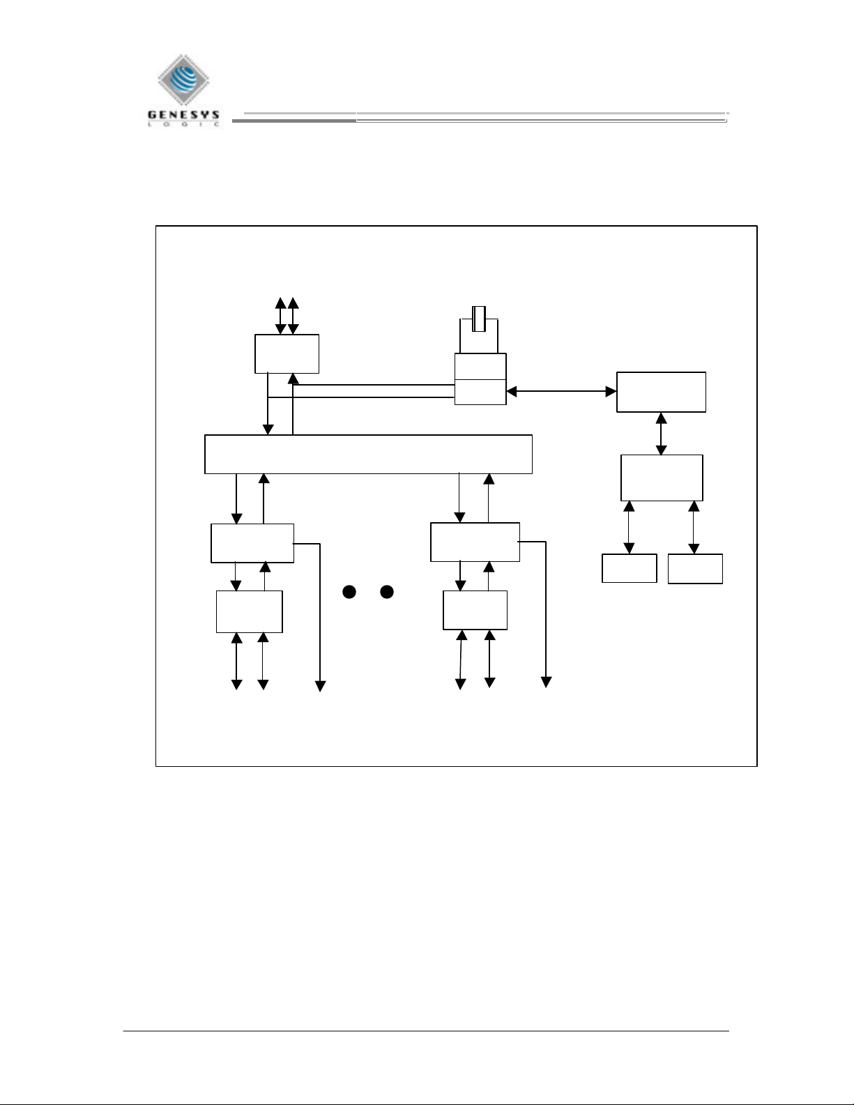
The GL652USB is an 8 port USB hub with 1 upstream port and 7 downstream ports. It
uses an 8-bit RISC-like uC to encode/decode the host commands. The GL652USB is
designed mainly for stand -alone hub and can also be integrated in PC motherboard or any
other devices to support USB hub function. The GL652USB can switch between selfpower and bus-power automatically without re-plug in. The GL652USB can be
configured as individual mode or ganged mode for the power management of
downstream port devices. To prevent from abnormal current consumption of downstream
port devices, the GL652USB supplies power enable flags by reading the over-current
flags. The GL652USB supports smart traffic indication through the LED lighting. The
higher data traffic flows through one port, the higher frequency of that port’s LED blinks.
To minimize the power consumption, the GL652USB will turn LED off and stop the
clock when they are suspended.
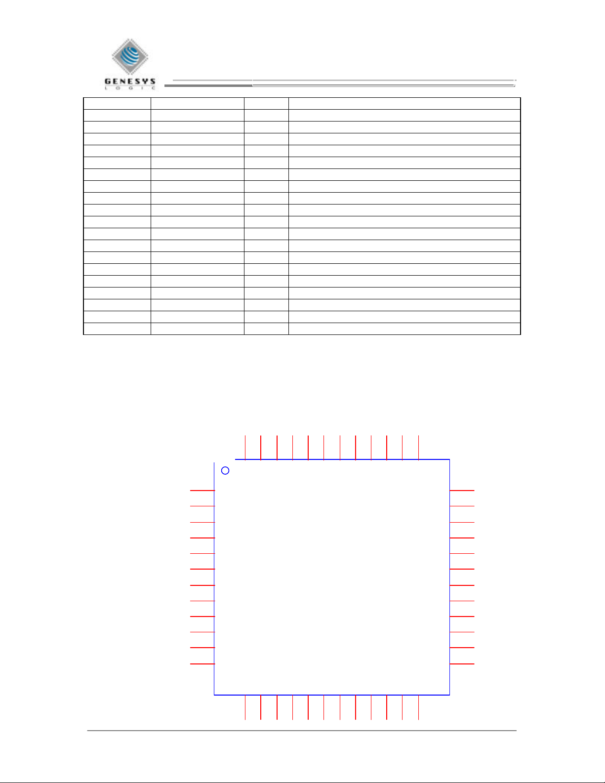
3 PIN DEFINITIONS AND DESCRIPTIONS
l GL652USB
Pin No. Name I/O Description
1 DP0 I/O Upstream port USB data+
2 DM0 I/O Upstream port USB data3 AGND - Analog ground
4 DP7 I/O Downstream port 7 USB data+
5 DM7 I/O Downstream port 7 USB data6 DP1 I/O Downstream port 1 USB data+
7 DM1 I/O Downstream port 1 USB data8 DP6 I/O Downstream port 6 USB data+
9 DM6 I/O Downstream port 6 USB data10 DP4 I/O Downstream port 4 USB data+
11 DM4 I/O Downstream port 4 USB data12 AVCC - Analog VCC(5V)
13 DP2 I/O Downstream port 2 USB data+
14 DM2 I/O Downstream port 2 USB data15 VCP - 3.3V output
16 DP5 I/O Downstream port 5 USB data+
17 DM5 I/O Downstream port 5 USB data18 DP3 I/O Downstream port 3 USB data+
19 DM3 I/O Downstream port 3 USB data20 SUSPND O Suspend indication output
21 SELF I 1: SELF-powered. 0: INDIVIDUAL-powered
22 LED1 O LED traffic indicator for downstream port 1
23 LED2 O LED traffic indicator for downstream port 2
24 LED3 O LED traffic indicator for downstream port 3
25 RESET I Reset input
26 LED4 O LED traffic indicator for downstream port 4
27 OVCUR4# I Over current flag for downstream port4
28 LED5 O LED traffic indicator for downstream port 5
3 08/18/00
Revision 1.2
Page 4
GL652USB 7 PORT USB HUB CONTROLLER
29 PWRENB4# O Power enable for downstream port 4
30 LED6 O LED traffic indicator for downstream port 6
31 PWRENB6# O Power enable for dow nstream port 6
32 TEST I Test mode input
33 OVCUR6# I Over current flag for downstream port6
34 XTAL2 O Ceramic resonator or crystal out
35 XTAL1 I Ceramic resonator or crystal in
36 DGND - Digital ground
37 PWRENB3# O Power enable for downstream por t 3
38 OVCUR3# I Over current flag for downstream port3
39 LED7 O LED traffic indicator for downstream port 7
40 OVCUR7# I Over current flag for downstream port7
41 DVCC - Digital VCC(5V)
42 OVCUR5# I Over current flag for downstream port5
43 PWRENB5# O Power enable for downstream port 5
44 PWRENB2# O Power enable for downstream port 2
45 PWRENB7# O Power enable for downstream port 7
46 OVCUR2# I Over current flag for downstream port2
47 PWRENB1# O Power enable for downstream port 1
48 OVCUR1# I Over current flag for downstream port1
Note 1: “#” means low active
Note 2: If using crystal, TEST pull low. If using oscillator, TEST pull high.
Table 1 GL652USB Pin Definitions and Descriptions
GL652USB
GL650USB
48
47
46
45
44
43
42
41
40
39
38
1
DP0
2
DM0
3
AGND
4
DP7
5
DM7
6
DP1
7
DM1
8
DP6
9
DM6
10
DP4
11
DM4
12
AVCC
OVRCUR1#
PWRENB1#
OVRCUR2#
PWRENB7#
PWRENB2#
PWRENB5#
DVCC
OVRCUR5#
LED7
OVRCUR7#
OVRCUR3#
OVRCUR6#
PWRENB6#
PWRENB4#
OVRCUR4#
37
DGND
PWRENB3#
XTAL1
XTAL2
TEST
LED6
LED5
LED4
RESET
36
35
34
33
32
31
30
29
28
27
26
25
4 08/18/00
13
DP2
DM214VCP
15
16
DP5
17
DM5
DP3
DM319SUSPND20SELF21LED122LED223LED3
18
24
Revision 1.2
Page 5
GL652USB 7 PORT USB HUB CONTROLLER
TRANSCEIVER
D+
D-
SIE
PLL
PORT CON-
TRANS-
DOWNSTREAM
D+
LED
DOWNSTREAM
PORT CON-
TRANSCEIVER
D-
LED
4 BLOCK DIAGRAM
UPSTREAM
PORT
TROLLER
CEIVER
D-
PORT 1
HUB REPEATER
12 MHz
TROLLER
D+
PORT 7
Registers
Controller
ROM
Micro-
RAM
5 08/18/00
Revision 1.2
Page 6
GL652USB 7 PORT USB HUB CONTROLLER
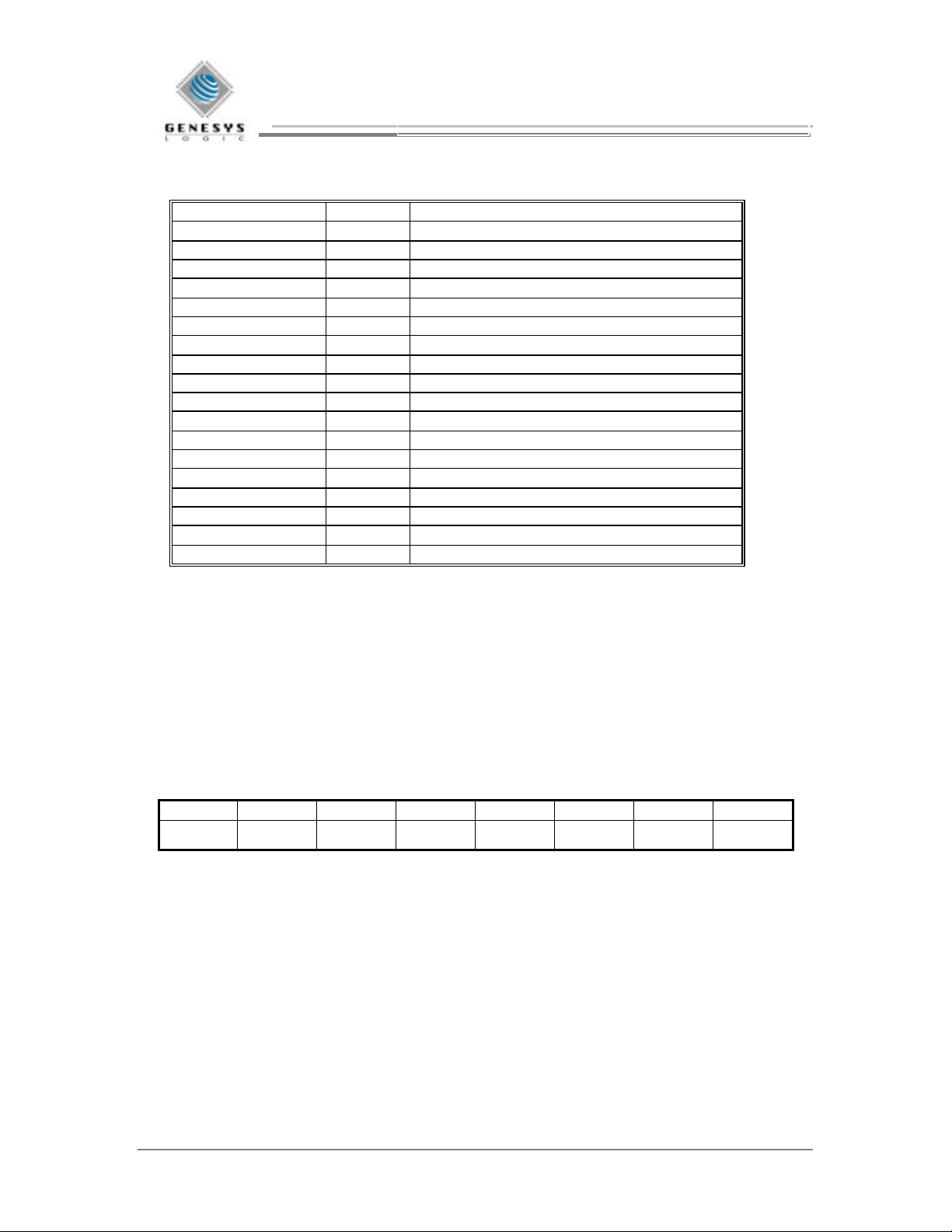
5 REGISTER SUMMARY
MNEMONIC OFFSET DESCRIPTION
DEVCTL 00h Device control register
EVTFLG 01h USB function interrupt flag
RXCTL0 02h Endpoint 0 RX control
TXCTL0 03h Endpoint 0 TX control
TXCTL1 04h Endpoint 1 TX control
FFDAT 05h Data buffer (FIFO) I/O port
BUFCTL 06h Data buffer control register
PORTSEL 07h Hub port to be configured
HUB_STAT_CHG 08h Hub status and status change indicator
PORT_STATUS 09h Hub ports status indicator
BUS_PORT_DATA 0Ah Hub ports status change indicator
HOST_CMD 0Bh Host command to downstream ports
ENP1_IND 0Ch Endpoint 1 indicator
TRXFLAG 0Dh Downstream port traffic flag
LED_INIT 0Eh LED initial state
GPIOD 0Fh General purpose I/O pin status
REV 10h Chip revision
DEVSTUS 11h USB device address and configuration status
Register Description
Terminology:
R/O: read only
R/W: read / write
R/W1C: read / write “1” to clear
W/O: write only
DEVCTL ( offset 00, default = 00h )
R/W R/W R/W R/O R/O
USBRDY SFRAME
USBRDY : 0 - USB interface is not ready. The device drives USB with SE0.
SFRAME : short frame option for test purpose
PWRDN : power down mode
PWRDN
1 - USB interface is ready. The device stops driving USB with SE0.
After power -on reset, USBRDY is cleared and the device looks like
disconnected. Set USBRDY to ‘1’ to enable USB interface.
Set SFRAME to ‘1’ will shorten frame length to 1/15 ms. It is to shorten the
time required for test.
-- -- -- SELF GANG
In suspend state, firmware can set PWRDN to put the controller into power
down mode. In this mode, the embedded micro-controller and most internal
activities are frozen. Hardware will automatically clear PWRDN upon
hardware reset or resume activities occur.
6 08/18/00
Revision 1.2
Page 7

GL652USB 7 PORT USB HUB CONTROLLER
SELF : 0 - HUB is bus powered.
1 - HUB is self powered.
GANG : 0 - HUB is in individual mode.
1 - HUB is in ganged mode.
EVTFLG ( offset 01, default = 00h )
R/W1C R/W1C R/W1C R/W1C R/W1C R/W1C R/W1C R/W1C
USBRST
Interrupt event flag –
EP0RX : a SETUP or OUT transaction to endpoint 0 is accepted
EP0TX : USB host controller accepts data transmitted via endpoint 0.
EP1TX : USB host controller accepts data transmitted via endpoint 1
SUSPD : the controller goes into suspend state
WAKEUP : remote wakeup is detected when global suspended
SOF : SOF detected or generated by HUB timer.
C_LCPWR : POWER source change.
USBRST : End of USB reset
RXCTL0 ( offset 02, default = 40h )
R/W R/O R/O R/O R/O R/O R/O R/O
RXDIS RXSETUP RXOUT RXSEQ RXCNT3 RXCNT2 RXCNT1 RXCNT0
Status of endpoint 0 recei ving –
RXCNT3~0 : EP0 received data byte count.
RXSEQ : 1 - The received data PID is DATA1
RXOUT : 1 - The received token PID is OUT.
RXSETUP : 1 - The received token PID is SETUP.
RXDIS : 0 - Endpoint 0 FIFO is empty and ready for data-packet receiving.
If RXDIS = 1, the device will not accept an OUT transaction addressed to it, and will respond
with a NAK to an error -free transaction. Hardware will automatically set RXDIS after a
successful receiving. After processing, the micro-controller should clear RXDIS to enable next
data-packet receiving or free FF0 for filling of the data to transmit. Note that a SETUP
transaction addressed to the device is always accepted even though RXDIS = 1.
TXCTL0 ( offset 03, default = 00h )
R/W R/W R/W R/W R/W R/W R/W
-- EP0STL EP0OE EP0SEQ EP0CNT3 EP0CNT2 EP0CNT1 EP0CNT0
Endpoint 0 transmit setting –
EP0CNT3~0 : number of data bytes to transmit
EP0OE : enable data transmit
EP0SEQ : data packet type
EP0STL : set endpoint 0 stall
1 – EP0 will respond to USB host controller with STALL packet
EP0STL will be automatically cleared when a setup transaction is accepted.
SOF C_LCPWR WAKEUP SUSPD EP1TX EP0TX EP0RX
0 - The received data PID is DATA0
1 - Endpoint 0 FIFO is filled with data and will reject the new -coming data
packet.
1 – ready to transmit data packet
0 – not ready to transmit data packet (default)
0 –DATA0
1 –DATA1
7 08/18/00
Revision 1.2
Page 8

GL652USB 7 PORT USB HUB CONTROLLER
After filling the data-to-transmit into FF0, the micro-controller should setup this register to
enable endpoint 0 data transmit. If EP0OE = 0, endpoint 0 will respond to a valid IN transaction
with a NAK. EP0OE will be automatically cleared after a successful transmission, or when
endpoint 0 has incidentally accepted another SETUP or OUT transaction.
TXCTL1 ( offset 04, default = 00h )
R/W R/W R/W R/O R/O R/O R/W
-- EP1STL EP1OE EP1SEQ EP1CNT3 EP1CNT2 EP1CNT1 EP1CNT0
Endpoint 1 transmit setting –
EP1CNT3~0 : number of data bytes to transmit. EP1CNT3~1 are always ‘0’.
EP1OE : enable data transmit
1 – ready to transmit data packet
0 – not ready to transmit data packet (default)
EP1SEQ : data packet type
0 –DATA0
1 –DATA1
EP1STL : set endpoint 1 stall
1 – EP1 will respond to USB host controller with STALL packet
0 – default
After preparing the data to transmit, the micro-controller should setup this register to enable
endpoint 1 data transmit. If EP1OE = 0, endpoint 1 will respond to a valid IN transaction with a
NAK. After a successful transmission, the device will automatically clear EP1OE.
FFDAT ( offset 05, default = 00h )
R/W R/W R/W R/W R/W R/W R/W R/W
FFD7 FFD6 FFD5 FFD4 FFD3 FFD2 FFD1 FFD0
If FFSEL1 (in BUFCTL) = 1’b0, this is FF0 access-window; if FFSEL1 = 1’b1, this is FF1
access-window. Each FFDAT read/write will automatically increase the FIFO pointer, which is
a 3-bit circular counter, by 1. Writing FPRST with ‘1’ (in BUFCTL) will reset the pointer. Note
that to fill FF0, RXDIS (in RXCTL0) must be first cleared.
BUFCTL ( offset 06 )
W/O R/W
-- -- -- -- -- FPRST -- FFSEL1
Data buffer control –
FFSEL1 : FIFO 0/1 selector
1’b0 – select endpoint 0 data buffer
1’b1 – select endpoint 1 data buffer
FPRST : reset FIFO 0/1 pointer (write only)
PORTSEL ( offset 07, default = 00h )
R/W R/W R/W R/W R/W R/W R/W
-- PORTSEL7 PORTSEL6 PORTSEL5 PORTSEL4 PORTSEL3 PORTSEL2 PORTSEL
PORTSEL : PORT 1~7 under request
PORTSEL1 1’b1 – port 1 selected
PORTSEL2 1’b1 – port 2 selected
PORTSEL3 1’b1 – port 3 selected
PORTSEL4 1’b1 – port 4 selected
PORTSEL5 1’b1 – port 4 selected
PORTSEL6 1’b1 – port 4 selected
PORTSEL7 1’b1 – port 4 selected
1
8 08/18/00
Revision 1.2
Page 9

GL652USB 7 PORT USB HUB CONTROLLER
HUB_STAT_CHG ( offset 08, default = 00h )
R/O R/O R/O R/O
LCPWR OVCUR -- -- -- -- C_LCPWR C_OVCUR
HUB status and status change
LCPWR : HUB local power status
1’b0 – local power good
1’b1 – local power lost
OVRCUR : HUB over current indicator
1’b0 – No over-current condition currently exists
1’b1 – A hub over-current condition exists
C_LCPWR : Local power status change
1’b0 – No change has occurred to local power status
1’b1 – local power status has changed
C_OVRCUR : HUB over current indicator change
1’b0 – No change has occurred to the over-current indicator
1’b1 – Hub over-current indicator has changed
PORT_STATUS ( offset 09, default = 00h )
R/O R/O R/O R/O R/O R/O R/O
PT_LOW_
SPD
Port status indicator:
PT_LOW_SPD : 1’b0 – full speed device connected, 1’b1 – low speed device
connected
PT_PWR : 1’b0 – port is in power off state, 1’b1 – port is not in power off state
PT_RST : 1’b0 – Reset signaling not asserted, 1b’1 – Reset signaling asserted
PT_OVCUR : 1’b0 – No over-current condition occurred on this port
1’b1 – An over-current condition exists on this port
PT_SUS : 1’b0 – port not suspended, 1’b1 – port suspended or resuming
PT_EN : 1’b0 – port is disabled, 1’b1 – port is enabled
PT_CON : 1’b0 – No device is present, 1’b1 – A device is present on this port
BUS_PORT_DATA ( offset 0A, default = 00h )
R/O R/O R/O R/O R/O R/O R/O
VP VM -- C_PT_RST C_PT_
Bus state and Port status change indicator:
VP : VP state on the downstream port
VM : VM state on the downstream port
C_PT_RST : 1’b0 – No change, 1’b1 – Reset complete
C_PT_OVCUR : 1’b0 – No change has occurred to over-current indicator
1’b1 – over-current indicator has changed
C_PT_SUS : 1’b0 – No change, 1’b1: – Resume complete
C_PT_EN : Set to one when a port is disabled because of a Port_error condition
C_PT_CON : 1’b0 – No change has occurred to current connect status
1’b1 – Current connect status has changed
HOST_CMD ( offset 0B, default = 0Fh )
W/O W/O W/O W/O W/O W/O W/O W/O
HB_CMD3 HB_CMD2 HB_CMD1 HB_CMD0 PT_CMD3 PT_CMD2 PT_CMD1 PT_CMD0
PT_PWR -- PT_RST PT_OVCUR PT_SUS PT_EN PT_CON
OVCUR
C_PT_
SUS
C_PT_EN C_PT_
CON
9 08/18/00
Revision 1.2
Page 10

GL652USB 7 PORT USB HUB CONTROLLER
Host command to the hub:
PT_CMD3~0 : 4’h0 –SetPortFeature(PORT_SUSPEND)
: 4’h1 –SetPortFeature(PORT_RESET)
: 4’h2 –SetPortFeature(PORT_POWER)
: 4’h3 –ClearPortFeature(PORT_ENABLE)
: 4’h4 –ClearPortFeature(PORT_SUSPEND)
: 4’h5 –ClearPortFeature(PORT_POWER)
: 4’h6 –ClearPortFeature(C_PORT_RESET)
: 4’h7 –ClearPortFeature(C_PORT_OVER_CURRENT)
: 4’h8 –ClearPortFeature(C_PORT_SUSPEND)
: 4’h9 –ClearPortFeature(C_PORT_ENABLE)
: 4’hA –ClearPortFeature(C_PORT_CONNECTION)
HB_CMD3 : 1’b1 –SetHubFeature(C_HUB_LOCAL_POWER)
HB_CMD2 : 1’b1 –SetHubFeature(C_HUB_OVER_CURRENT)
HB_CMD1 : 1’b1 –ClearHubFeature(C_HUB_LOCAL_POWER)
HB_CMD0 : 1’b1 –ClearHubFeature(C_HUB_OVER_CURRENT)
ENP1_IND ( offset 0C, default = 00h )
R/O R/O R/O R/O R/O R/O R/O R/O
PT7 PT6 PT5 PT4 PT3 PT2 PT1 HUB
Endpoint 1 interrupt change indicator
TRXFLAG ( offset 0D, default = 00h )
R/W1C R/W1C R/W1C R/W1C R/W1C R/W1C R/W1C
-- P7_TRX P6_TRX P5_TRX P4_TRX P3_TRX P2_TRX P1_TRX
Upstream traffic flag:
P1_TRX : upstream traffic happens on downstream port 1
P2_TRX : upstream traffic happens on downstream port 2
P3_TRX : upstream traffic happens on downstream port 3
P4_TRX : upstream traffic happens on downstream port 4
P5_TRX : upstream traffic happens on downstream port 5
P6_TRX : upstream traffic happens on downstream port 6
P7_TRX : upstream traffic happens on downstream port 7
LED_INIT ( offset 0E, default = 00h )
R/W1C R/W1C R/W1C R/W1C R/W1C R/W1C R/W1C
-- P7_ON P6_ON P5_ON P4_ON P3_ON P2_ON P1_ON
LED initial flag:
P1_ON : if 1’b1, LED is always on, otherwise, judge according to TRXFLAG
register.
P2_ON : if 1’b1, LED is always on, otherwise, judge according to TRXFLAG
register.
P3_ON : if 1’b1, LED is always on, otherwise, judge according to TRXFLAG
register.
P4_ON : if 1’b1, LED is always on, otherwise, judge according to TRXFLAG
register.
P5_ON : if 1’b1, LED is always on, otherwise, judge according to TRXFLAG
register.
P6_ON : if 1’b1, LED is always on, otherwise, judge according to TRXFLAG
register.
P7_ON : if 1’b1, LED is always on, otherwise, judge according to TRXFLAG
register.
10 08/18/00
Revision 1.2
Page 11

GL652USB 7 PORT USB HUB CONTROLLER
GPIOD (offset 0F, default = 0Fh)
R/W R/W R/W R/W R/W R/W R/W
-- GPIO6D/
LED7
GPIO5D/
GPIO4D/
LED5
GPIO3D/
LED4#
GPIO2D/
LED3#
GPIO1D/
LED2#
GPIO0D/
LED1#
LED6
General purpose I/O pin status –
If GPIOXOE = 1 (X: 0 ~ 6), GPIOX is driven with the level of internal GPIOXD latch, which
is the same as corresponding GPIOXD bit. If GPIOXOE = 0, GPIOXD reflects the level of
GPIOX pin, which may be different from internal GPIOXD latch. The value written to GPIOD
will be stored in an internal latch, no matter what direction the GPIOX pins are in. Bits 6 to 0
have been pre-assigned specific functions for LED indicators. (active low).
REV ( offset 10, default = current revision )
R/O R/O R/O R/O R/O R/O R/O R/O
REV7 REV6 REV5 REV4 REV3 REV2 REV1 REV0
This register returns current silicon revision number of the HUB.
Current revision is 8’h11. (Revision 1.1)
DEVSTUS ( offset 11, default = 00h )
R/W R/W R/W R/W R/W R/W R/W R/W
HCONFIG DEVADR6 DEVADR5 DEVADR4 DEVADR3 DEVADR2 DEVADR1 DEVADR0
USB device status registers. Procedure to set the device address:
1. After USB reset, the device responds to default address 0, and hub configuration = 0.
2. USB host controller issues SET_ADDRESS request to the device. (INTRB asserted)
3. Micro-contro ller recognizes the request, then set DEVADR register with appropriate value.
4. Micro-controller prepares the status stage of SET_ADDRESS request by programming
TXCTL0 register.
5. When the hub configuration value is not equal zero, HCONFIG is set to one.
USB reset will clear this register.
6 MAXIMUM RATINGS
Maximum ratings are the extreme limits to which the GL652USB can be exposed without permanently
damaging it. The GL652USB contains circuitry to protect the inputs against damage from high static
voltages; however, do not apply voltages higher than those shown in the table. Keep VIN and V
the range GND ≤ (VIN or V
) ≤ VCC. Connect unused inputs to the appropriate voltage level, either GND
OUT
OUT
or VDD.
Symbol Characteristic Value Unit
T
Storage temperature -55 to +150
STG
TOP Operating temperature 0 to +70
°C
°C
VCC Supply voltage -0.5 to +7.0 V
VIN DC input voltage -0.5 to +V
+ 0.5 V
DD
I Maximum current per pin excluding VDD and VSS 25 mA
I
Maximum current out of GND 100 mA
MGND
I
Maximum current out of VCC 100 mA
MVCC
V
Static discharge voltage >4000 V
ESD
7 ELECTRICAL CHARACTERISTICS
within
11 08/18/00
Revision 1.2
Page 12

GL652USB 7 PORT USB HUB CONTROLLER
Symbol Parameter Tese Conditions Min. Typ. Max. Unit
Supply
VDD Digital Power Supply 4.5 5.0 5.5 V
V
Analog Power Supply 4.5 5.0 5.5 V
DDA
IDD Digital Supply Current mA
I
Analog Supply Current mA
DDA
USB Bus: DP and DM
VCP Regulated Voltage Output 3.0 3.3 3.6 V
VDI Static Input Voltage 0 - VCP V
VDO Static Output Voltage 0 - VCP V
Digital I/O Pins
VIL Input Logic Low Voltage - - 0.8 V
VIH Input Logic High Voltage 2.0 - - V
VOL Output Logic Low Voltage IO=-4.0mA - - 0.1xVDD V
VOH Output Logic High Voltage IO=+4.0mA 0.9xVDD - - V
12 08/18/00
Revision 1.2
Page 13

GL652USB 7 PORT USB HUB CONTROLLER
8 PACKAGE DIAGRAM
SYVBOIS MIN MAX
A 1.6
A1 0.05 0.15
A2 1.35 1.45
C1 0.09 0.16
D 9.00BSC
D1 7.00BSC
E 9.00BSC
E1 7.00BSC
48-LQFP
e 0.5BSC
b 0.17 0.27
L 0.45 0.75
L1 1 REF
D
D1
E1
E
b
e
0.25
L
L1
A1
13 08/18/00
C1
A2
A
Revision 1.2
Page 14

A
9. Application Circuits (1)
4 4
B
C
D
E
B_VCC
C1
0.1U
DP0
DM0
3 3
DP7
DM7
DP1
DM1
DP6
DM6
B_VCC
DP4
DM4
C4
OVRCUR1#
U1
4847464544434241403938
1
DP0
2
DM0
3
AGND
4
DP7
5
DM7
6
DP1
7
DM1
8
DP6
9
DM6
10
DP4
11
DM4
12
AVCC
0.1U
+
C5
2 2
C6
0.1U
4.7U
1314151617181920212223
DP2
GL652USB
PWRENB1#
OVRCUR1#
PWRENB1#
DP2
DM2
DM2
PWRENB7#
OVRCUR2#
OVRCUR2#
VCP
DP5
VCP
PWRENB2#
PWRENB7#
PWRENB2#
DP5
DM5
DM5
OVRCUR5#
PWRENB5#
PWRENB5#
DP3
DP3
DM3
DVCC
OVRCUR5#
DM3
SUSPND
SUSPEND
LED7
OVRCUR7#
OVRCUR7#
SELF
LED1
SELF
OVRCUR3#
LED7
OVRCUR6#
PWRENB6#
PWRENB4#
OVRCUR4#
LED1
LED2
PWRENB3#
37
DGND
OVRCUR3#
PWRENB3#
XTAL1
XTAL2
TEST
LED6
LED5
LED4
RESET
LED2
LED3
24
LED3
C2
30P
36
35
34
33
32
31
30
29
28
27
26
25
R11 1M
R1 1M
Y1 12 MHz
XTAL1
R6 24
OVRCUR6#
PWRENB6#
LED6
PWRENB4#
LED5
OVRCUR4#
LED4
R10 10K
C3
30P
B_VCC
B_VCC
LED1
LED2
LED3
LED4
LED5
LED6
LED7
D1
LED
D2
LED
D3
LED
D4
LED
D5
LED
D6
LED
D7
LED
R2 1K
R3 1K
R4 1K
R5 1K
R7 1K
R8 1K
R9 1K
VOUT1
VOUT2
VOUT3
VOUT4
VOUT5
VOUT6
VOUT7
1 1
Title
CIRCUIT FOR GENESYS 7-PORT USB HUB
Size Document Number Rev
USBHUB.DSN 1.2
B
A
B
C
D
Date: Sheet of
1 4Thursday, August 17, 2000
E
Page 15

A
9. Application Circuits (2)
B
C
D
E
VCC
B_VCC
B_VCC
4 4
S_VCC
R17
1M
B_VCC
PWRENB1#
R16
4.7K
G
DS
Q1
Q2
2N7002
D S
TP0610T
R18
MIC 29302
U3
G
FLG1#
FLG2#
PWRENB2#
U2
1
ENA#
OUTA#
2
FLGA#
FLGB#
ENB# OUTB#
MIC2526-8
IN
GND
3
4 5
VOUT1
8
7
6
VOUT2
C7
0.1U
VCC
4.7K
C12
47U
12345
R21 825K,%1
R24
267K,%1
REN
S_VCC
C11
3 3
POWER JACK
A 6V adapter is
recommended.
J1
0.1U
VCC
VCC
C13
0.1U
PWRENB3#
FLG3#
FLG4#
PWRENB4#
U4
1
ENA#
OUTA#
2
FLGA#
FLGB#
ENB# OUTB#
MIC2526-8
IN
GND
3
4 5
VOUT3
8
7
6
VOUT4
C10
0.1U
R12
10K
FLG1# FLG2#
R14 10K
OVRCUR1#
C8
0.1U
B_VCC
R19
10K
FLG3# FLG4#
R22 10K
OVRCUR3# OVRCUR4#
C14
0.1U
B_VCC
R13
10K
R15 10K
R20
10K
R23 10K
C9
0.1U
C15
0.1U
OVRCUR2#
VCC
B_VCC B_VCC
PWRENB5#
FLG5#
FLG6#
2 2
REN
S_VCC
MIC 29302
U6
12345
VCC
R31 825K,%1
R32
VCC
B_VCC
Q3
FDN340P
D S
SELF
G
R30
Q4
DS
2N7002
1M
R29
470
DS
REN
Q5
2N7002
G
G
267K,%1
PWRENB6#
PWRENB7# VOUT7
FLG7#
B_VCC
1 1
U5
1
ENA#
OUTA#
2
FLGA#
FLGB#
ENB# OUTB#
MIC2526-8
U7
ENA#
OUTA#
FLGA#
FLGB#
ENB# OUTB#
MIC2526-8
IN
GND
IN
GND
3
4 5
1
2
3
4 5
VOUT5
8
7
6
VOUT6
8
7
6
C16
0.1U
VCC
C19
0.1U
R25
10K
FLG5# FLG6#
R27 10K
OVRCUR5# OVRCUR6#
C17
0.1U
B_VCC
R33
10K
FLG7#
R34 10K
C20
0.1U
OVRCUR7#
R26
10K
R28 10K
C18
0.1U
A
Title
CIRCUIT FOR GENESYS 7-PORT USB HUB
Size Document Number Rev
USBHUB.DSN 1.2
Custom
B
C
D
Date: Sheet of
2 4Thursday, August 17, 2000
E
Page 16

A
9. Application Circuits (3)
B
C
D
E
VCP B_VCC
R35
4 4
VOUT1
+
C26
3 3
120U
VOUT2
+
C30
120U
DM0
DP0
C24
47P
L5 FB
L7 FB
L9 FB
C25
47P
1.5K
C28
0.1U
C32
0.1U
R38 22
R39 22
DM1
DP1
DM2
DP2
L11 FB
2 2
R42 22
R44 22
R50 22
R52 22
L2 FB
L4 FB
R46
15K
R54
15K
C21 10U
+
R47
15K
R55
15K
J3
1
2
3
4
USB-B
J4
1
2
3
4
USB-A
J6
1
2
3
4
USB-A
VOUT4
VOUT5
VOUT6
L1 FB
DM4
R36 22
DP4
+
C22
120U
L3 FB
C23
0.1U
R37 22
R40
15K
L6 FB
DM5
R43 22
+
C27
120U
L8 FB
C29
0.1U
DP5
R45 22
R48
15K
L10 FB
DM6
R51 22
+
C31
120U
L12 FB
C33
0.1U
DP6
R53 22
R56
15K
R41
15K
R49
15K
R57
15K
J2
1
2
3
4
USB-A
J5
1
2
3
4
USB-A
J7
1
2
3
4
USB-A
VOUT3
L13 FB
DM3
R58 22
+
C34
120U
L15 FB
C36
0.1U
DP3
R60 22
R62
15K
1 1
A
B
R63
15K
J8
1
2
3
4
USB-A
VOUT7
C
L14 FB
DM7
R59 22
DP7
+
C35
120U
L16 FB
C37
0.1U
R61 22
R64
15K
D
J9
1
2
3
4
USB-A
R65
15K
Title
CIRCUIT FOR GENESYS 7-PORT USB HUB
Size Document Number Rev
USBHUB.DSN 1.2
B
Date: Sheet of
3 4Thursday, August 17, 2000
E
Page 17

A
9. Application Circuits (4)
4 4
B
C
D
E
Description
1. First Product Release '00/04/05
1.0
1. Seperate 4-port and 7-port hubs into different schematic files.1.1
2. Omit the ganged mode pull-up resistor on 'SUSPND' pin.
3. Add a 10K pull-up resistor to 'RESET' pin.
4. Connect pin 1 of U3 to B_VCC, then regulator will be enabled
only when upstream port is plugged!
A 1M pull-low resistor is also added to disable this pin when
the upstream port is not plugged.
5. 'SELF' is directly connected to drain of Q4 to omit the external
3 3
2 2
debounce RC circuit for this pin.
6. Q1 is replaced by a more popular and cheaper one -- FDN340P.
7. Some resistor values are increased to save the operating current.
switch output.
2. Remove the 47U output capacitor of MIC29302 to suppress inrush current.
3. Add R1, R6 and C6 for EMI suppressing.
4. Change C22, C26, C27, C30, C31, C34 and C35 from 100U to 120U for
better behavior in droop test.
5. Add a 2-transistor circuit for regulator ENABLE pin. That will save
several tens of mA operating current than direct connecting B_VCC
to ENABLE pin.
6. Remove a redudant transistor in SELF-BUS power switching circuit.
7. Change MIC29512 to 2 paralell MIC29302 for better driving capability.
DateRev.
'00/05/18
'00/08/171.2 1. Change the pull-up voltage source for each LED from B_VCC to power
1 1
Title
CIRCUIT FOR GENESYS 7-PORT USB HUB
Size Document Number Rev
USBHUB.DSN 1.2
B
A
B
C
D
Date: Sheet of
4 4Thursday, August 17, 2000
E
 Loading...