

Page 1

GL660USB -
Genesys Logic, Inc.
USB2.0 to IEEE-1284 / DMA Bridge
SPECIFICATION 1.1
June 29, 2001
Genesys Logic, Inc.
10F, No.11, Ln.3, Tsao Ti Wei, Shenkeng, Taipei, Taiwan
Tel: 886-2-2664-6655 Fax: 886-2-2664-5757
http://www.genesyslogic.com
Page 2

GL660USB - USB2.0 to IEEE-1284/DMA Bridge Controller
Contents
1 OVERVIEW..................................................................................................... 3
2 FEATURES ..................................................................................................... 4
3 FUNCTION BLOCK ........................................................................................ 5
3.1 B
LOCK DIAGRAM.............................................................................................5
3.2 F
UNCTIONAL DESCRIPTIONS ............................................................................ 6
4 SYSTEM CONFIGURATION .......................................................................... 7
4.1 IEEE1284 M
4.2 DMA M
ODE ...........................................................................................7
ODE.................................................................................................... 7
5 PIN INFORMATION ........................................................................................ 8
5.1
IEEE-1284 MODE ..........................................................................................8
5.1.1 Pin Assignments ................................................................................................ 8
5.1.2 Pin Descriptions................................................................................................. 9
5.2 DMA
5.2.1 Pin Assignments .............................................................................................. 10
5.2.2 Pin Descriptions............................................................................................... 11
MODE ..................................................................................................10
6 MODE CONFIGURATION ............................................................................12
7 REGISTER MAP........................................................................................... 13
8 ELECTRICAL CHARACTERISTICS ............................................................. 14
8.1 A
BSOLUTE MAXIMUM RATING S ....................................................................... 14
8.2 DC C
8.3 DC C
8.4 S
HARACTERISTICS (DIGITAL PINS)............................................................ 14
HARACTERISTICS (D+/D-) .....................................................................15
WITCHING CHARACTERISTICS....................................................................... 15
8.5 IEEE-1284 MODE TIMING CHART.................................................................. 16
8.5.1 Burst EPP Data Write (8-bit Mode) .................................................................. 16
8.5.2 Burst EPP Data Read (8-bit Mode).................................................................. 16
8.5.3 Burst EPP Data Write (16-bit Mode) ................................................................ 17
8.5.4 Burst EPP Data Read (16-bit Mode)................................................................ 18
9 PACKAGE DIMENSION................................................................................ 19
10 REVISION HISTORY ................................................................................ 20
©2000-2001 Genesys Logic Inc.—All rights reserved. Page 2 of 20
Page 3

GL660USB - USB2.0 to IEEE-1284/DMA Bridge Controller
1 Overview
GL660USB is a high performance USB 2.0 controller with integrated UTMI
transceiver proposed by Intel. Two operation modes, 1284 and DMA are
supported for kinds of application.
For 1284 mode, it is a bridge between USB bus and IEEE-1284 interface. By
adding GL660USB to parallel port device like printer and scanner, it’s very easy to
upgrade the original design into USB 2.0 interface.
For DMA mode, GL660USB can be used to replace some DMA controller like
NCR 53C80. That means it is easy to modify a SCSI device into USB 2.0 interface.
Four endpoints, control, bulk in, bulk out, and interrupt, are supported to satisfy
most USB application. Built in 2 sets of 512-byte ping-pong FIFOs to provide the
maximum performance. With extended 16-bit EPP/DMA bus, up to 40M-bytes/sec
transfer rate is reachable. Using 12MHz crystal and slew-rate controlled pads to
reduce EMI problem. With embedded CPU and customized firmware, GL660USB
provides maximum flexibility for customers. Additional 7 GPIOs can be
programmed to fit different applications.
GL660USB is compatible to GL640USB, the USB1.1 controller, in function. For
GL640USB customers, It’s easy to upgrade their original USB1.1 device without
software modification, only changing GL640USB and little modification in circuit is
needed.
©2000-2001 Genesys Logic Inc.—All rights reserved. Page 3 of 20
Page 4

GL660USB - USB2.0 to IEEE-1284/DMA Bridge Controller
2 Features
Supports two operating mode:
1. USB 2.0 to IEEE1284 bridge
2. USB 2.0 to DMA bridge
Complies with USB Specification Revision2.0
Supports 4 endpoints: Control (0) / Bulk Read(1) / Bulk Write(2) / Interrupt(3)
512- and 64-bytes of data payload for respective Bulk and Control endpoints.
8-bit Standard 1284-/DMA interface with max. 20M bytes/sec transfer rate
16-bit Extended EPP/DMA interface with max. 40M bytes/sec transfer rate
Separated ping-pong FIFO for bulk read/write transfer
Embed a 7.5 MIPS CPU to provide maximum flexibility
Supports power down mode and suspend indicator
7 additional GPIOs controlled by SW/FW (IEEE1284 mode only)
12MHz crystal input
Function compatible to GL640USB controller
Available in 48 pin LQFP package
©2000-2001 Genesys Logic Inc.—All rights reserved. Page 4 of 20
Page 5

GL660USB - USB2.0 to IEEE-1284/DMA Bridge Controller
3 Function Block
3.1 Block Diagram
GPI01-7
RPU
CLK30
DPF
DPH
RXSTS
USB 2.0
UTMI
TXCTL
SIE
TXCVR
LOGIC
16
DMF
DMH
DATA
RREF
CLK120
Mode
Selector
TEST0 SUSPND
64-byte CTLFIFO
CPU Control Register
CLK15
ASTRB_
4
WR_
DSTRB_
VALIDH
512-byte TXFIFO0
8-/16-Bit
EPP15-0
512-byte TXFIFO1
Engine
EPP/DMA
WAIT_
512-byte RXFIFO0
512-byte RXFIFO1
24-60MHZ
CLKOUT
120MHZ
X10
PLL
clkgen
480MHZ
X40
12MHZ
PLL
©2000-2001 Genesys Logic Inc.—All rights reserved. Page 5 of 20
Page 6

GL660USB - USB2.0 to IEEE-1284/DMA Bridge Controller
3.2 Functional Descriptions
3.2.1 USB2.0 Transceiver
The analog circuitry to handle the USB HS/FS signaling.
3.2.2 UTMI Logic
The UTMI Logic is compliant to Intel‘s UTMI specification 1.01. This block handles the
low level USB protocol and signaling, which including data and clock recovery, NRZI
encoding/decoding, Bit Stuffing/De-stuffing, supporting USB2.0 test modes and
serial/parallel conversion.
3.3.3 PLL
10XPLL provides the 120MHz clock output for UTMI Logic block. UTMI operates in
120MHz for USB HS data processing. 40XPLL block will provide 480MHz for USB HS
data transmission.
3.3.4 CLKGEN
This is the clock generator block for the logic blocks. It generates 15MHz clock for
micro controller, 24MHz ~ 60MHz for EPP engine, 30MHz clock for UTMI, SIE, and
FIFO.
3.3.5 CPU
It is a 15MHz 8-bit micro controller, the brain of GL660USB. After receiving a USB
command, CPU processes command data and re-assigns tasks to EPP/DMA engine,
GPIOs, FIFO. Then it will response proper data/status to USB host.
3.3.6 EPP/DMA Engine
EPP/DMA engine is extended from standard IEEE1284/DMA protocol. It supports
normal 8-bit EPP/ECP data accessing with up to 20M-bytes/s transfer rate. With
extended 16-bit mode, VALIDH is used for the control of high byte. Up to 40Mbytes/sec transfer rate can be achieved.
3.3.7 FIFOs
TXFIFO0/TXFIFO1 is a 512-byte ping-pong FIFOs for ‘bulk read’ purpose. It buffers
data from EPP/DMA engine, and re-directs to USB SIE logic.
RXFIFO0/RXFIFO1 is a 512-byte ping-pong FIFOs for ‘bulk write’ purpose. It buffers
data from USB SIE logic, and send to EPP/DMA engine for I/O write operation..
CTLFIFO is a 64-byte FIFO for control endpoint. Operations of ‘control write’ and
‘control read’ use CTLFIFO as data buffer. CPU accesses CTLFIFO for command
processing and status responding.
3.3.8 Control Registers
Control Register configures GL660USB to proper operation. For example, CPU can
set registers to generate wakeup event, enter suspend, transmit proper USB packet to
host.
©2000-2001 Genesys Logic Inc.—All rights reserved. Page 6 of 20
Page 7

r
GL660USB - USB2.0 to IEEE-1284/DMA Bridge Controller
4 System Configuration
4.1 IEEE1284 Mode
IEEE-1284
ASIC
HS-EPP
GL660USB
USB2 Bus
4.2 DMA Mode
CPU
DMA
Controlle
CPUBUS
DMABUS
GL660USB
USB2 Bus
©2000-2001 Genesys Logic Inc.—All rights reserved. Page 7 of 20
Page 8

GL660USB - USB2.0 to IEEE-1284/DMA Bridge Controller
5 Pin Information
5.1 IEEE-1284 Mode
5.1.1 Pin Assignments
36
35
34
33
32
37
38
39
40
41
42
43
44
45
46
47
48
EPPD8
EPPD9
EPPD10
EPPD11
DVCC1
DGND1
EPPD12
EPPD13
EPPD14
EPPD15
GPIO6
GPIO7
EPPD7
EPPD6
EPPD4
EPPD5
GL660USB
IEEE-1284 MODE
GPIO1
HRSTZ
GPIO2
3
SUSPND
4
5
1
2
31
DVCC0
DGND0
RPU
AVCC0
6
30
EPPD3
DPF
7
29
EPPD2
DPH
8
28
EPPD1
DMF
9
27
EPPD0
DMH
10
26
WRZ
AGND0
11
25
VALIDH
CLKOUT
DSTRBZ
ASTRBZ
AGND1
AVCC1
RREF
12
WAITZ
GPIO5
GPIO4
GPIO3
TEST0
XO
24
23
22
21
20
19
18
17
16
15
XI
14
13
©2000-2001 Genesys Logic Inc.—All rights reserved. Page 8 of 20
Page 9

GL660USB - USB2.0 to IEEE-1284/DMA Bridge Controller
5.1.2 Pin Descriptions
Pin
#
1 GPIO1 B up General Purpose I/O
2 HRSTZ I up Chip reset Input, active low
3 GPIO2 B up General Purpose I/O
4 SUSPND O down USB suspend indicator
5 RPU - 3.3V Pull up control for DPF
6 AVCC0 P Positive analog supply (3.3V)
7 DPF B Positive USB differential data (Full Speed)
8 DPH B Positive USB differential data (High Speed)
9 DMF B
10 DMH B Negative USB Differential Data (High Speed)
11 AGND0 P Analog ground (0V)
12 RREF - 510Ohm reference resistor input
13 AVCC1 P Positive analog supply (3.3V)
14 XO B Crystal output
15 XI I 12MHz crystal/oscillator input
16 AGND1 P Analog ground (0V)
17 TEST0 I down Test mode enable
18 GPIO3 B up General purpose I/O
19 GPIO4 B down General purpose I/O
20 ASTRBZ O EPP Address strobe
21 GPIO5 B General Purpose I/O
22 DSTRBZ O EPP data strobe
23 CLKOUT O 24-60MHz clock output
24 WAITZ I EPP acknowledge input
25 VALIDH O High byte valid
26 WRZ O EPP write indicator
27 EPPD 0 B EPP Data bus 0
28 EPPD 1 B EPP data bus 1
29 EPPD 2 B EPP data bus 2
30 EPPD 3 B EPP data bus 3
31 DVCC0 P Positive digital supply (3.3V)
32 DGND0 P Digital ground (0V)
33 EPPD 4 B EPP data bus 4
34 EPPD 5 B EPP data bus 5
35 EPPD 6 B EPP data bus 6
36 EPPD 7 B EPP data bus 7
37 EPPD 8 B EPP data bus 8
38 EPPD 9 B EPP data bus 9
39 EPPD 10 B EPP data bus 10
40 EPPD 11 B EPP data bus 11
41 DVCC1 P Positive digital supply (3.3V)
42 DGND1 P Digital ground (0V)
43 EPPD 12 B EPP data bus 12
44 EPPD 13 B EPP data bus 13
45 EPPD 14 B EPP data bus 14
46 EPPD 15 B EPP data bus 15
47 GPIO6 B General purpose I/O
48 GPIO7 B General purpose I/O
Name I/O Pull
Up/Down
Description
Negative USB Differential Data (Full Speed)
It’s available only in 16-bit EPP mode
©2000-2001 Genesys Logic Inc.—All rights reserved. Page 9 of 20
Page 10

GL660USB - USB2.0 to IEEE-1284/DMA Bridge Controller
5.2 DMA mode
5.2.1 Pin Assignments
37
D8
38
D9
39
D10
40
D11
41
DVCC1
42
DGND1
43
D12
44
D13
45
D14
46
D15
47
A1
48
A2
36
D4
D5
D6
D7
DGND0
D3
DVCC0
GL660USB
DMA MODE
30
31
32
33
34
35
1
CSZ
HRSTZ
EOPZ
INTZ
RPU
AVCC0
DPF
2
3
4
5
6
7
29
8
D2
DPH
28
9
D1
DMF
27
10
D0
DMH
26
11
IORZ
AGND0
25
VALIDH
CLKOUT
DACKZ
AGND1
AVCC1
RREF
12
IOWZ
A3
A0
A4
DRQ
TEST0
XO
24
23
22
21
20
19
18
17
16
15
XI
14
13
©2000-2001 Genesys Logic Inc.—All rights reserved. Page 10 of 20
Page 11

GL660USB - USB2.0 to IEEE-1284/DMA Bridge Controller
5.2.2 Pin Descriptions
Pin
#
1 CSZ I up Chip select, active low
2 HRSTZ I up Chip reset Input, active low
3 EOPZ I up End of DMA cycles, active low
4 INTZ O down Interrupt output, active low
5 RPU - 3.3V Pull up control for DPF
6 AVCC0 P Positive analog supply (3.3V)
7 DPF B
8 DPH B
9 DMF B
10 DMH B
11 AGND0 P Analog ground (0V)
12 RREF - 510Ohm reference resistor input
13 AVCC1 P Positive analog supply (3.3V)
14 XO B Crystal output
15 XI I 12MHz crystal/oscillator input
16 AGND1 P Analog ground (0V)
17 TEST0 I down Test mode enable
18 DACKZ I up DMA acknowledge, active low
19 DRQ O down DMA request, active high
20 A4 I Address bus 4
21 A0 I Address bus 0
22 A3 I Address bus 3
23 CLKOUT O 24-60MHz clock output
24 IOWZ I Write strobe input, active low
25 VALIDH I High byte valid
26 IORZ I Read strobe input, active low
27 D 0 B Data bus 0
28 D 1 B Data bus 1
29 D 2 B Data bus 2
30 D 3 B Data bus 3
31 DVCC0 P Positive digital supply (3.3V)
32 DGND0 P Digital ground (0V)
33 D 4 B Data bus 4
34 D 5 B Data bus 5
35 D 6 B Data bus 6
36 D 7 B Data bus 7
37 D 8 B Data bus 8
38 D 9 B Data bus 9
39 D 10 B Data bus 10
40 D 11 B Data bus 11
41 DVCC1 P Positive digital supply (3.3V)
42 DGND1 P Digital ground (0V)
43 D 12 B Data bus 12
44 D 13 B Data bus 13
45 D 14 B Data bus 14
46 D 15 B Data bus 15
47 A1 B Address bus 1
48 A2 B Address bus 2
Name I/O Pull
Up/Down
Negative USB Differential Data (Full Speed)
Description
Positive USB differential data (Full Speed)
Positive USB differential data (High Speed)
Negative USB Differential Data (High Speed)
Available only input 16-bit mode
©2000-2001 Genesys Logic Inc.—All rights reserved. Page 11 of 20
Page 12

GL660USB - USB2.0 to IEEE-1284/DMA Bridge Controller
6 Mode Configuration
GL660USB decides its operating modes at the rising edge of HRSTZ, or chip
is exiting the reset state. At this moment, PIN24 and PIN26 are used to set
the operating mode. The following table shows the relationship among
operating modes and WRZ/WAITZ configuration.
Operating Modes PIN24 PIN26
IEEE-1284 Mode Pull Down Pull Up
DMA mode Pull Up Pull Up
©2000-2001 Genesys Logic Inc.—All rights reserved. Page 12 of 20
Page 13
GL660USB - USB2.0 to IEEE-1284/DMA Bridge Controller
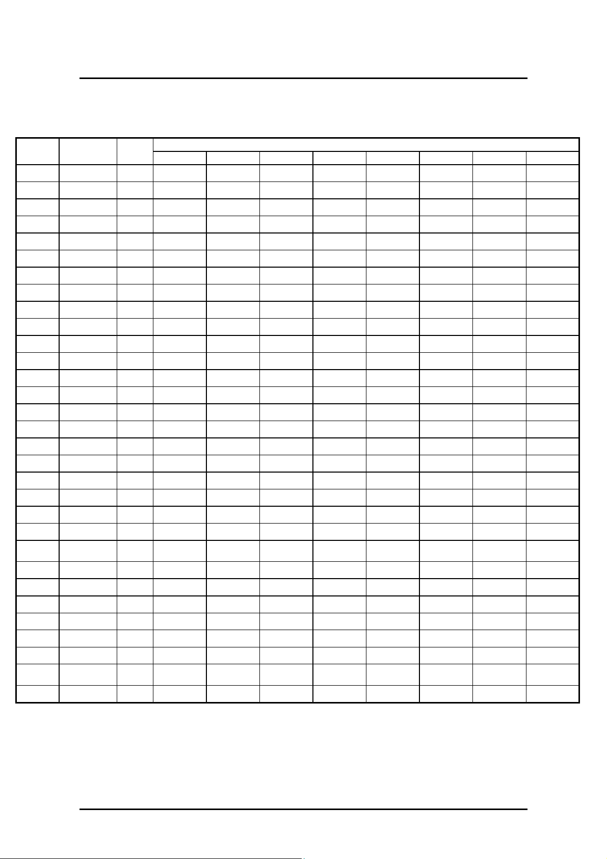
7 Register Map
Address Mnemonic
00h DEVCTL0 10 HS_SUS CHIRPEN EP0TXSTL DISGLUSB EP0RXSTL WAKEDIS PWRDN
01h EVTFLG 00 CHIRPDET URST WAKEUP RESUME SUSPD EP0TX EP0RX
02h DEVADR 00 DEVADR6 DEVADR5 DEVADR4 DEVADR3 DEVADR2 DEVADR1 DEVADR0
03h RXCTL0 0x RXDIS0 RXSETUP RXOUT RXSEQ
04h TXCTL0 00 TXOE TXSEQ
05h CTLDAT xx CTLD7 CTLD6 CTLD5 CTLD4 CTLD3 CTLD2 CTLD1 CTLD0
06h MISC 00 SUSPD ADDR DEFAULT POWER TSTEPP FFRST0 SF SUSDIS
07h GPIO 00 GPIO7 GPIO6 GPIO5 GPIO4 GPIO3 GPIO2 GPIO1
08h GPIOCTL 00 GPIOEN7 GPIOEN6 GPIOEN5 GPIOEN4 GPIOEN3 GPIOEN2 GPIOEN1
09h UTMDATL 00 UTMD7 UTMD6 UTMD5 UTMD4 UTMD3 UTMD2 UTMD1 UTMD0
0Ah UTMDATH 00 UTMD15 UTMD14 UTMD13 UTMD12 UTMD11 UTMD10 UTMD9 UTMD8
0Bh UTMCTL 0C LINEST1 LINEST0 OPMOD1 OPMOD0 FSPEED HSTERM_ TXVLDH TXVLD
0Ch RXFF0LEN 00 RF0LEN7 RF0LEN6 RF0LEN5 RF0LEN4 RF0LEN3 RF0LEN2 RF0LEN1 RF0LEN0
0Dh RXFF1LEN 00 RF1LEN7 RF1LEN6 RF1LEN5 RF1LEN4 RF1LEN3 RF1LEN2 RF1LEN1 RF1LEN0
0Eh RX0CNT 00 FF0LEN6 FF0LEN5 FF0LEN4 FF0LEN3 FF0LEN2 FF0LEN1 FF0LEN0
10h DEVCTL1 00 EN_CLKO CKSEL2 CKSEL1 CKSEL0
11h ENDPCTL 00 EPEN3 EPEN2 EPEN1 EPSTL3 EPSTL2 EPSTL1
12h EPPCTL0 78 WAIT_ DSTRB_ ASTRB_ WR_ NC NC MODE16
13h INTFLG 00 RESUME SUSPND AUTOEND TSTPKTX EP3TX DATARX DATATX
14h UINTEN 00 REMINTEN SUSINTEN ATINTEN TPKINTEN EP3INTEN DRXINTEN DTXINTEN
15h Reserved
16h EP3DAT 00 EP3D7 EP3D6 EP3D5 EP3D4 EP3D3 EP3D2 EP3D1 EP3D0
17h FFSEL
Def
(Hex)
00 RX0FFPSH TX0FFPOP TX1FFSEL TX0FFSEL TXFFPSH RX1FFSEL RX0FFSEL RXFFPSH
B7 B6 B5 B4 B3 B2 B1 B0
BIT
18h FFCFG 00 TX512 ECP ATORXEN ATOTXEN
19h FFCTL 00 FF0RST RXFFRST TXFFRST EP3TXEN DTX1EN DTX0EN TSTPKEN TSTPKRST
1Ah TXFFDAT xx TXFFD7 TXFFD6 TXFFD5 TXFFD4 TXFFD3 TXFFD2 TXFFD1 TXFFD0
1Bh RXFFDAT xx RXFFD7 RXFFD6 RXFFD5 RXFFD4 RXFFD3 RXFFD2 RXFFD1 RXFFD0
1Ch ATOLENL xx ATOLEN7 ATOLEN6 ATOLEN5 ATOLEN4 ATOLEN3 ATOLEN2 ATOLEN1 ATOLEN0
1Dh ATOLENH xx ATOLEN15 ATOLEN14 ATOLEN13 ATOLEN12 ATOLEN11 ATOLEN10 ATOLEN9 ATOLEN8
1Eh EPPCTL1
1Fh EPPAD xx EPPAD7 EPPAD6 EPPAD5 EPPAD4 EPPAD3 EPPAD2 EPPAD1 EPPAD0
80 NORMEPP ADOE
©2000-2001 Genesys Logic Inc.—All rights reserved. Page 13 of 20
Page 14

GL660USB - USB2.0 to IEEE-1284/DMA Bridge Controller
8 Electrical Characteristics
8.1 Absolute Maximum Ratings
SYMBOL Description MIN MAX
VCC DC supply voltage -0.5V +3.6V
VI DC input voltage -0.5V VCC+0.5V
V
DC input voltage range for I/O -0.5V VCC+0.5V
I/O
V
DC input voltage for USB D+/D- pins -0.5V VCC+0.5V
AI/O
V
DC voltage applied to outputs in High Z state -0.5V VCC+0.5V
I/OZ
V
Static discharge voltage 4000V
ESD
TA Ambient Temperature 0 oC 100
o
C
8.2 DC Characteristics (Digital Pins)
SYMBOL Description MIN TYP MAX UNIT
PD Power Dissipation mA
VDD Power Supply Voltage 3 3.3 3.6 V
IO DC output sink current excluding D+/D-
/VCC/GND
VIL LOW level input voltage 0.9 V
VIH HIGH level input voltage 2.0 V
V
LOW to HIGH threshold voltage 1.3 1.43 1.56 V
TLH
V
HIGH to LOW threshold voltage 1.3 1.43 1.56 V
THL
V
Hysteresis voltage - 0 - V
HYS
VOL LOW level output voltage when IOL=8mA 0.4 V
VOH HIGH level output voltage when IOH=8mA 2.4 V
I
Leakage current for pads with internal
OLK
pull up or pull down resistor
8 mA
46 µA
RDN Pad internal pull down resister (Note 1) 79K 105K 152K Ohms
RUP Pad internal pull up resister (Note 2) 78K 104K 146K Ohms
©2000-2001 Genesys Logic Inc.—All rights reserved. Page 14 of 20
Page 15

GL660USB - USB2.0 to IEEE-1284/DMA Bridge Controller
8.3 DC Characteristics (D+/D-)
SYMBOL Description MIN TYP MAX UNIT
VOL D+/D- static output LOW (RL of 1.5K to
0.3 V
3.6V )
VOH D+/D- static output HIGH (RL of 15K to
2.8 3.6 V
GND )
VDI Differential input sensitivity 0.2 V
VCM Differential common mode range 0.8 2.5 V
VSE Single-ended receiver threshold 0.2 V
CIN Transceiver capacitance 20 pF
ILO Hi-Z state data line leakage -10 +10 µA
Z
Driver output resistance 28 43 Ohms
DRV
8.4 Switching Characteristics
SYMBOL Description MIN TYP MAX UNIT
FX1 X1 crystal frequency 11.97 12 12.03 MHz
T
X1 cycle time 83.3 ns
CYC
T
X1 clock LOW time 0.45T
X1L
T
X1 clock HIGH time 0.45T
X1H
T
Output pad rise time from 10% to 90%
r30pf
cyc
cyc
ns
ns
ns
swing with 30pF loading
T
Output pad fall time from 10% to 90%
f30pf
ns
swing with 30pF loading
T
Output pad rise time from 10% to 90%
r50pf
ns
swing with50pF loading
T
Output pad fall time from 10% to 90%
f50pf
ns
swing with 50pF loading
T
D+/D- rise time with 50pF loading 4 20 ns
rUSB
T
D+/D- fall time with 50pF loading 4 20 ns
fUSB
©2000-2001 Genesys Logic Inc.—All rights reserved. Page 15 of 20
Page 16

GL660USB - USB2.0 to IEEE-1284/DMA Bridge Controller
8.5 IEEE-1284 Mode Timing Chart
8.5.1 Burst EPP Data Write (8-bit Mode)
T0
DSTRB_
T2
WR_
WAIT_
IOD7-0
T1
T4
Symbol Description Min Max Unit
T0 DSTRB_ low to WR_ low 0 1.5 ns
T1 WR_ low to IOD7-0 valid 15 ns
T3
T2 WAIT_ high to DSTRB_ high 0.5 T 1.5 T T=1/f
T3 WAIT_ low to DSTRB_ low 1.5 T 2.5 T T=1/f
T4 WR_ high to IOD7-0 invalid 0 ns
8.5.2 Burst EPP Data Read (8-bit Mode)
DSTRB_
WAIT_
IOD7-0
Symbol Description Min Max Unit
T0 IOD7-0 Setup Time 10 ns
T2
T3
T1
T0
T1 IOD7-0 Hold Time 0 ns
T2 WAIT_ high to DSTRB_ high 0.5 T 1.5 T T=1/f
T3 WAIT_low to DSTRB_low 1.5 T 2.5 T T=1/f
©2000-2001 Genesys Logic Inc.—All rights reserved. Page 16 of 20
Page 17
GL660USB - USB2.0 to IEEE-1284/DMA Bridge Controller
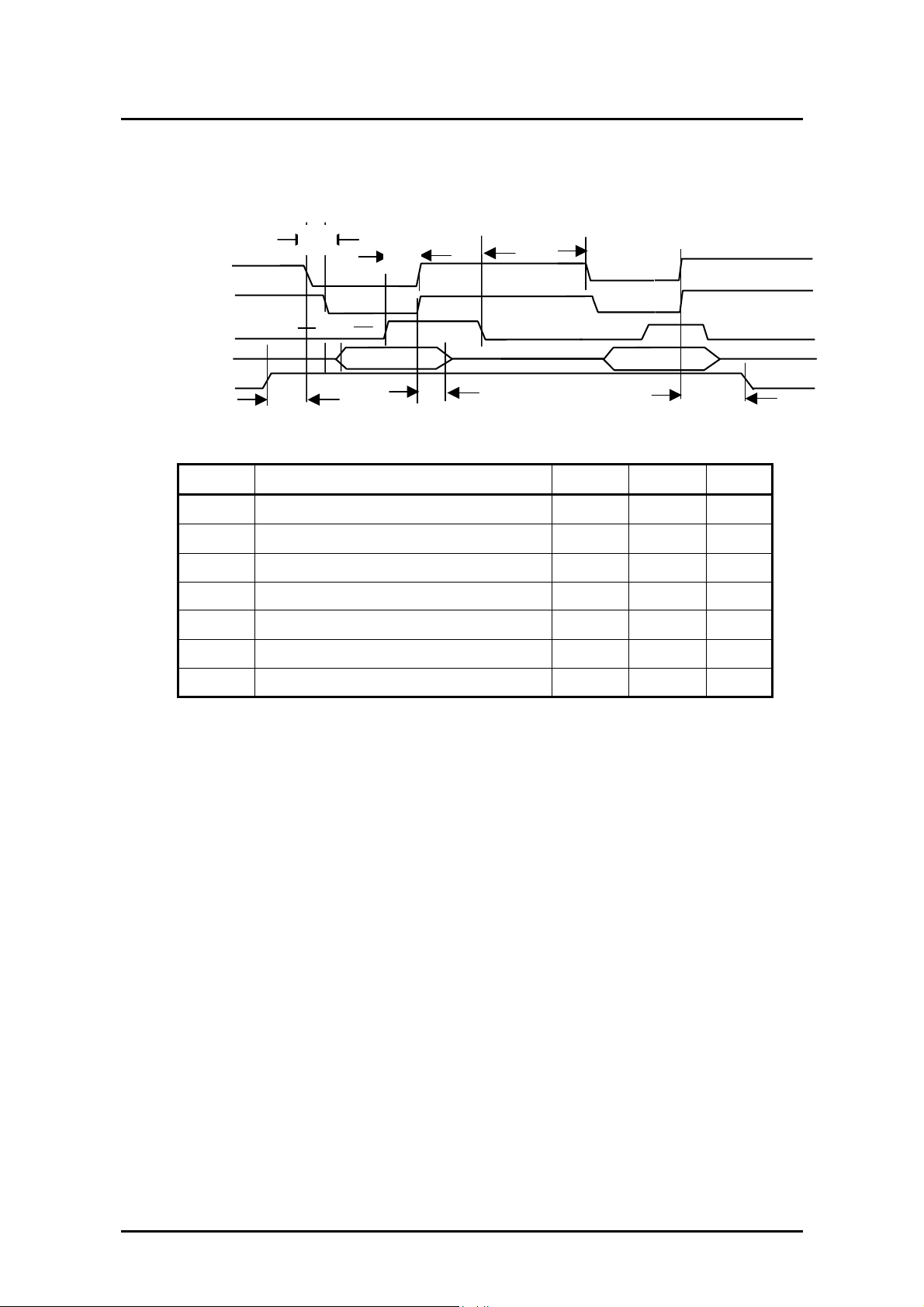
8.5.3 Burst EPP Data Write (16-bit Mode)
DSTRB_
WR_
T0
T2
T3
WAIT_
T1
IOD15-0
VALID H
T4
T5
T6
Symbol Description Min Max Unit
T0 DSTRB_ low to WR_ low 0 1.5 ns
T1 WR_ low to IOD15-0 valid 15 ns
T2 WAIT_ high to DSTRB_ high 0.5T 1.5T 1/f
T3 WAIT_ low to DSTRB_ low 1.5T 2.5T 1/f
T4 VALIDH high to DSTRB_ low 1T 1T 1/f
T5 WR_ high to IOD15-0 invalid 0 ns
T6 DSTRB_ high to VALIDH low 2T 2T 1/f
©2000-2001 Genesys Logic Inc.—All rights reserved. Page 17 of 20
Page 18

GL660USB - USB2.0 to IEEE-1284/DMA Bridge Controller
8.5.4 Burst EPP Data Read (16-bit Mode)
DSTRB_
WR_
WAIT_
IOD15-0
VALID H
T4
T2
T0
T1
Symbol Description Min Max Unit
T0 IOD15-0 valid to DSTRB_ high 10 ns
T3
T5
T1 DSTRB_ high to IOD15-0 invalid 0 ns
T2 WAIT_ high to DSTRB_ high 1/2 T 3/2 T 1/f
T3 WAIT_ low to DSTRB_ low 3/2 T 5/2 T 1/f
T4 VALIDH high to DSTRB_ low T T 1/f
T5 DSTRB_ high to VALIDH low 2T 2T 1/f
©2000-2001 Genesys Logic Inc.—All rights reserved. Page 18 of 20
Page 19

GL660USB - USB2.0 to IEEE-1284/DMA Bridge Controller
9 Package Dimension
SYMBOL MIN MAX
A 1.6
A1 0.05 0.15
A2 1.35 1.45
C1 0.09 0.16
D 9.00BSC
D1 7.00BSC
E 9.00BSC
E1 7.00BSC
e 0.5BSC
b 0.17 0.27
L 0.45 0.75
L1 1 REF
©2000-2001 Genesys Logic Inc.—All rights reserved. Page 19 of 20
Page 20

GL660USB - USB2.0 to IEEE-1284/DMA Bridge Controller
10 Revision History
Version Description Date
1.0 First draft 2000/10/25
1.1 Added IEEE1284 mode Timing chart. 2001/06/29
©2000-2001 Genesys Logic Inc.—All rights reserved. Page 20 of 20
 Loading...