

Page 1

GL620USB-A
GeneLink
USB PC-to-PC Networking
Controller
SPECIFICATION 1.6
Nov 17, 2000
Genesys Logic, Inc.
10F, No.11, Ln.3, Tsao Ti Wei, Shenkeng, Taipei, Taiwan
Tel: 886-2-2664-6655 Fax: 886-2-2664-5757
http://www.genesyslogic.com
Your Imagination, Our Creation
Page 2

Revision 1.6 Nov. 17, 2000
-2-
GL620USB-A
Index
1. Features ............................................................................................................................ 3
2. Functional Overview........................................................................................................4
3. Applications...................................................................................................................... 5
4. Functional Description..................................................................................................... 6
5. Driver Support.................................................................................................................. 8
6. Pin Definitions and Descriptions.................................................................................... 10
7. Electrical Characteristics.................................................................................................11
7.1 Absolute Maximum Ratings (Voltages referenced to GND)..................................................................11
7.2 DC Characteristics (VCP/D+/D-)........................................................................................................11
7.3 DC Characteristics (PIN1, 2)...............................................................................................................11
7.4 DC Characteristics (PIN10, 11) ..........................................................................................................12
7.5 DC Characteristics (PIN14, 15).......................................................................................................... 12
7.6 Switching Characteristics.................................................................................................................... 12
8. Package Diagram............................................................................................................13
9. Application Circuit......................................................................................................... 14
Page 3

Revision 1.6 Nov. 17, 2000
-3-
GL620USB-A
1. Features
l Conforms to USB 12Mbps Specification, Version 1.1
l Patented architecture
l Single chip solution for host-to-host communication
l Network driver (NDIS standard) support running on Windows 98 and Windows 2000
l Support TCP/IP, NetBEUI, IPX/SPX protocols
l Up to 8.6Mbps transfer rate
l Suitable for mobile and SOHO environment
l Tiniest solution in the market – 16-pin SOP
l On-chip 3.3V output
l 12MHz external clock
l Internal power-on reset
l Power management support
Page 4
Revision 1.6 Nov. 17, 2000
-4-
GL620USB-A
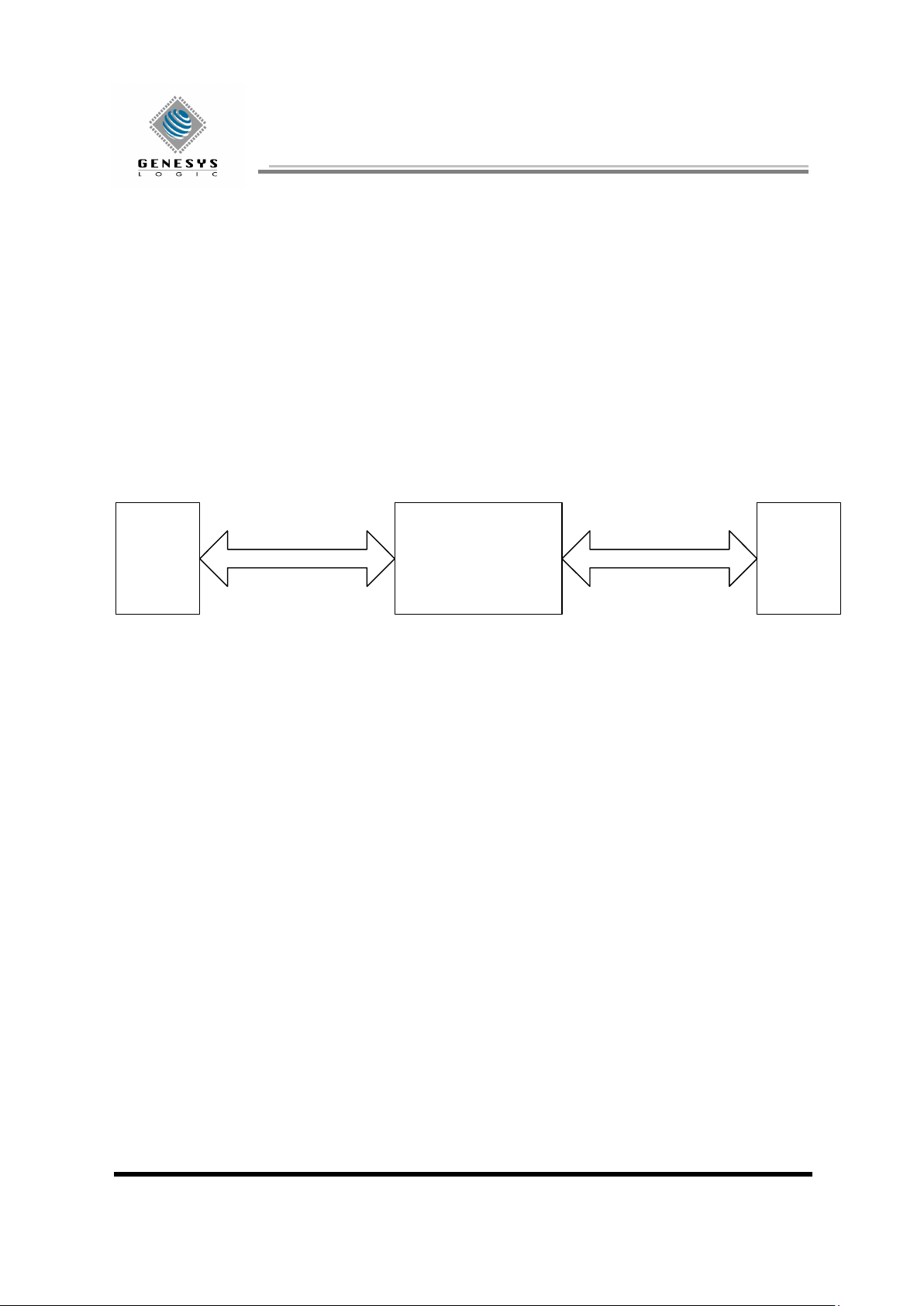
2. Functional Overview
The GL620USB-A provides a single-chip solution for networking two or more PCs via their USB ports.
According to USB protocol, the PC is the host and the device is a slave, where the host initiates all the USB traffic
and the slave responds to the host ’s requests. In other words, a host cannot talk to another host via USB protocol;
instead, a host can only talk to one or more devices. The GL620USB-A’s patent-pending architecture overcomes
the USB inherently incompatibility of connecting two or more PCs by providing two independent USB
transceivers and SIEs for each host, i.e., data can be transferred in both directions simultaneously.
System Diagram
GL620USB-A
PC A PC B
USB Connection USB Connection
Page 5

Revision 1.6 Nov. 17, 2000
-5-
GL620USB-A
3. Applications
The windows network driver software comes with GL620USB-A can connect 2 or more PCs via USB ports easily.
Genesys Logic also provides Macintosh driver software for GL620USB-A and supports the direct connection
between two Macintosh machines. The plug-and-play nature of USB protocol makes the installation and usage of
end products very simple.
Working with a full-featured windows driver, the GL620USB-A can perform the following functions between
two or more PCs:
l File transfer
l Ethernet emulation
l Storage device sharing: hard drive, CD-ROM, floppy, …
l Printer sharing
l Internet sharing
Working with a full-featured Macintosh driver, the GL620USB-A can perform the following functions between
two Macintosh machines:
l Ethernet emulation
l Storage device sharing: hard drive, CD-ROM, floppy, …
l Printer sharing
Working with GL620USB-A and its Windows/Macintosh drivers, PC can provide Internet sharing to Macintosh.
GL620USB-A doesn’t support file transfer/sharing function between PC and Macintosh except that the extra
third-party software is installed.
The GL620USB-A networking function can be integrated with the following form factors:
l USB standalone cable
l USB standalone hub
l USB monitor with hub
l PC host
Page 6

Revision 1.6 Nov. 17, 2000
-6-
GL620USB-A
4. Functional Description
Block diagram of GL620USB-A
The GL620USB-A is equipped with two full-speed USB ports, and each port has four endpoints to provide
different functions as follows:
Endpoint 0: control transfer
Endpoint 1: bulk-read transfer
Endpoint 2: bulk-write transfer
Endpoint 3: interrupt transfer
Two 8-bytes FIFO and four 64-bytes FIFO are built in the device as follows:
- Left 8-byte FIFO: provide a pipe to link left endpoint 0 and right endpoint 3. For example, if left host wants
to communicate with right host, left host can issue a no data control transfer and the setup command will be
64 Byte FIFO
64 Byte FIFO
8 Byte FIFO
8 Bytes FIFO
USB
Interface
USB
Interface
Micro-
controller
USB Registers
&
FIFO Control
D+
D-
D+
D-
Page 7

Revision 1.6 Nov. 17, 2000
-7-
GL620USB-A
stored in the left 8-byte FIFO. Right host can request an interrupt transfer to get the setup command from
left host. The status stage of the left side control transfer will not be terminated until the right side get the
setup command via interrupt transfer.
- Right 8-byte FIFO: provide a pipe to link right endpoint 0 and left endpoint 3.
- Left 64-bytes DATA0/DATA1 FIFOs: provide a pipe to link left endpoint 2 and right endpoint 1. For
example, if left host wants to transfer data to right host, left host can issue bulk write transfer and the
payload will be stored in the left 64-byte FIFOs. Right host can request a bulk read transfer to get the data
from left host.
- Right 64-bytes DATA0/DATA1 FIFOs: provide a pipe to link right endpoint 2 and left endpoint 1.
Page 8

Revision 1.6 Nov. 17, 2000
-8-
GL620USB-A
5. Driver Support
The Genesys Logic Ethernet Driver is a mini-port device driver emulating a network interface running on
Windows 98 and Windows 2000. The Genesys Logic Ethernet Driver conforms to the NDIS (Network Driver
Interface Specification) standard. The users can use standard Windows utilities such as Windows Explorer,
Network Neighborhood and standard file sharing security features. Even though there’s no Ethernet card present,
the Genesys Logic Ethernet Driver performs all the functions an Ethernet card can do, and more, the
plug-and-play feature. The users can build up their own private network by connecting several PCs via the
GL620USB-A embedded cables.
The Genesys Logic software router is a network protocol layer driver. The software router can forward packet
between the GL620USB-A embedded cable and Ethernet LAN to emulate all PCs on the network build by
GL620USB-A is also on the Ethernet LAN. This function can share all resources on Ethernet LAN to
GL620USB-A connected PCs.
The Genesys Logic Ethernet Macintosh Driver is a device driver emulating a network interface running on Mac
OS 8.5, 8.6 and 9.0. After enable the standard Macintosh file sharing service, the users can share the device
resources such as HD, CD-ROM between two Macintosh machines by the Macintosh Network Browser.
Page 9

Revision 1.6 Nov. 17, 2000
-9-
GL620USB-A
Computer A
Computer B
Computer C
Printer
Computer D
Ethernet LAN
GL620USB-A
Cable
Genesys Logic software router is running
on Computer B
NDIS driver for GL620USB-A are
Functional equivalent
Computer B
Computer C
Printer
Computer D
Ethernet LAN
Computer A
Page 10

Revision 1.6 Nov. 17, 2000
-10-
GL620USB-A
6. Pin Definitions and Descriptions
PIN SYMBOL I/O DESCRIPTION
1 GPIO1 B General purpose IO pin / Driving LED capability
2 GPIO2 B General purpose IO pin / Driving LED capability
3 LVM B Left D4 LVP B Left D+
5 VCP O 3.3V output
6 RVP B Right D+
7 RVM B Right D8 AGND - Ground
9 DGND - Ground
10 OSCSEL I Selection of clock type
11 EXTRST_ I External reset
12 XTAL1 I 12M crystal input
13 XTAL2 O Crystal output
14 GPIO3 B General purpose IO pin
15 GPIO4 B General purpose IO pin
16 VCC - 5V power
1
2
3
4
14
7
6
5
VCC
OSCSEL
XTAL2
AGND
RVM
GPIO1
EXTRST_
LVM
13
10
12
11
9
8
DGND
GPIO2
GPIO3
GPIO4
LVP
XTAL1
RVP
VCP
16
15
16-pin SOP
Page 11

Revision 1.6 Nov. 17, 2000
-11-
GL620USB-A
7. Electrical Characteristics
7.1 Absolute Maximum Ratings (Voltages referenced to GND)
SYMBOL Description MIN MAX
VCC DC supply voltage -0.5V +7V
VI DC input voltage -0.5V VCC+0.5V
V
I/O
DC input voltage range for bidirect pins -0.5V VCC+0.5V
V
AI/O
DC input voltage for USB D+/D- pins(PIN3, 4, 6, 7) -0.5V VCC+0.5V
V
I/OZ
DC voltage applied to outputs in High Z state -0.5V VCC+0.5V
V
ESD
static discharge voltage 4000V
7.2 DC Characteristics (VCP/D+/D-)
SYMBOL Description MIN TYP MAX UNIT
V
3.3
VCP regulator output 3.0 3.3 3.6 V
I
3.3
VCP maximum supply current 27 41 56 mA
VOL D+/D- static output LOW(RL of 1.5K to 3.6V ) 0.3 V
VOH D+/D- static output HIGH (RL of 15K to GND ) 2.8 3.6 V
VDI Differential input sensitivity 0.2 V
VCM Differential common mode range 0.8 2.5 V
VSE Single-ended receiver threshold 0.2 V
CIN Transceiver capacitance 20 pF
ILO Hi-Z state data line leakage -10 +10
µA
Z
DRV
Driver output resistance 28 43 Ohms
7.3 DC Characteristics (PIN1, 2)
SYMBOL Description MIN TYP MAX UNIT
VDD Power Supply Voltage 4.5 5.0 5.5 V
IOL DC output sink current at 0.4V 13.01 19.54 24.82 mA
IOH DC output source current at VDD -0.4V 6.35 9.82 12.37 mA
I
OHTTL
DC output source current at TTL high 24.62 49.45 69.12 mA
VIL LOW level input voltage 0.7 V
VIH HIGH level input voltage 2.66 V
V
TLH
LOW to HIGH threshold voltage 2.02 2.38 2.66 V
V
THL
HIGH to LOW threshold voltage 0.7 0.83 1.0 V
V
HYS
Hysteresis voltage 1.1 1.55 1.79 V
VOL LOW level output voltage when IOL=16mA 0.4 V
Page 12

Revision 1.6 Nov. 17, 2000
-12-
GL620USB-A
7.4 DC Characteristics (PIN10, 11)
SYMBOL Description MIN TYP MAX UNIT
VDD Power Supply Voltage 4.5 5.0 5.5 V
VIL LOW level input voltage 0.69 V
VIH HIGH level input voltage 2.65 V
V
TLH
LOW to HIGH threshold voltage 2.01 2.37 2.65 V
V
THL
HIGH to LOW threshold voltage 0.69 0.82 0.99 V
V
HYS
Hysteresis voltage 1.1 1.55 1.79 V
RUP Pad internal pullup resister 191.27 240.69 376.34 Kohms
7.5 DC Characteristics (PIN14, 15)
SYMBOL Description MIN TYP MAX UNIT
VDD Power Supply Voltage 4.5 5.0 5.5 V
IOL DC output sink current at 0.4V 3.89 5.94 7.56 mA
IOH DC output source current at VDD -0.4V 2.85 4.36 5.46 mA
I
OHTTL
DC output source current at TTL high 10.9 21.5 29.75 mA
VIL LOW level input voltage 0.71 V
VIH HIGH level input voltage 2.68 V
V
TLH
LOW to HIGH threshold voltage 2.03 2.39 2.68 V
V
THL
HIGH to LOW threshold voltage 0.71 0.83 1.0 V
V
HYS
Hysteresis voltage 1.1 1.55 1.8 V
VOL LOW level output voltage when IOL=4mA 0.4 V
RDN Pad internal pulldown resister 122.08 160 267.31 Kohms
7.6 Switching Characteristics
SYMBOL Description MIN TYP MAX UNIT
FX1 X1 crystal frequency 11.97 12 12.03 MHz
T
CYC
X1 cycle time 83.3 ns
T
X1L
X1 clock LOW time 0.45T
cyc
ns
T
X1H
X1 clock HIGH time 0.45T
cyc
ns
T
r30pf
Output pad rise time from 10% to 90% swing with 30pF
loading
6 8 12 ns
T
f30pf
Output pad fall time from 10% to 90% swing with 30pF
loading
5.3 7 10.4 ns
T
r50pf
Output pad rise time from 10% to 90% swing with50pF
loading
9.5 13 19 ns
T
f50pf
Output pad fall time from 10% to 90% swing with 50pF
loading
7.7 10 16 ns
T
rUSB
D+/D- rise time with 50pF loading 4 20 ns
T
fUSB
D+/D- fall time with 50pF loading 4 20 ns
Page 13

Revision 1.6 Nov. 17, 2000
-13-
GL620USB-A
8. Package Diagram
Dimension in mils Dimension in mm
Symbol
Min Nom Max Min Nom Max
A --- 58 --- --- 1.473 --A1 6 --- --- 0.152 --- --A2 --- 24 --- --- 0.610 ---
B --- 16 --- --- 0.406 ---
C --- 8 --- --- 0.203 ---
D 388 390 392 9.855 9.906 9.957
E1 152 154 156 3.861 3.912 3.962
e --- 50 --- --- 1.270 ---
eB --- 238 --- --- 6.045 ---
L 25 --- --- 0.635 --- --θ
0° 3° 6° 0° 3° 6°
A2
A1
B
e
A
D
C
eB
E1
L
θ
Page 14

Revision 1.6 Nov. 17, 2000
-14-
GL620USB-A
9. Application Circuit
 Loading...