

Page 1

Genesys Logic, Inc.
GL603USB
Genesys Logic, Inc.
GL603USB-A
GL603USB-B
USB + PS/2 MOUSE
MICROCONTROLLER
SPECIFICATION 1.4
Sep 22, 2000
10F, No.11, Ln.3, Tsao Ti Wei, Shenkeng, Taipei, Taiwan
Tel: 886-2-2664-6655 Fax: 886-2-2664-5757
http://www.genesyslogic.com
Page 2

GL603USB/GL603USB-A/GL603USB-B
TABLE OF CONTENTS
1 FEATURES ............................................................................................................................................................4
2 FUNCTIONAL OVERVIEW ...........................................................................................................................6
3 PIN DEFIN ITIONS AND DESCRIPTIONS ................................................................................................7
3.1 GL603USB ......................................................................................................................................................7
3.2 GL603USB-A ..................................................................................................................................................9
3.3 GL603USB-B ................................................................................................................................................11
4 FUNCTIONAL DESCRIPTION....................................................................................................................12
4.1 MEMORY ORGANIZATION......................................................................................................................12
4.1.1 Program Memory Organization ...................................................................................................12
4.1.2 Data Memory Organization ........................................................................................................... 12
4.2 USB FUNCTION REGISTERS..................................................................................................................13
4.3 MCU FUNCTION REGISTERS ................................................................................................................16
4.4 FULL-RANGE DETECTION AND ANALOG -TO-DIGITAL CONVERTER.....................................20
4.5 CLOCK GENERATOR................................................................................................................................21
4.6 GENERAL PURPOSE I/O PORTS ...........................................................................................................21
4.7 TIMER INTERRUPT ...................................................................................................................................22
4.8 USB ENGINE................................................................................................................................................22
4.8.1 Voltage Regulator .............................................................................................................................22
4.8.2 USB Transceiver................................................................................................................................22
4.8.3 Serial Interface Engine (SIE).........................................................................................................24
4.9 INSTRUCTION SET SUMMARY..............................................................................................................25
4.9.1 Operand Field Descriptions ...........................................................................................................25
4.9.2 Instruction Set....................................................................................................................................25
5 ABSOLUTE MAXIMUM RATINGS ...........................................................................................................27
6 ELECTRICAL CHARACTERISTICS........................................................................................................34
7 PACKAGE DIAGRAMS ..................................................................................................................................36
7.1 16-pin P-DIP.................................................................................................................................................36
7.2 18-pin P-DIP.................................................................................................................................................37
7.3 20-pin P-DIP.................................................................................................................................................38
7.4 16-pin SOP....................................................................................................................................................39
7.5 18-pin SOP....................................................................................................................................................40
7.6 20-pin SOP....................................................................................................................................................41
2 09/22/00
Revision 1.4
Page 3

GL603USB/GL603USB-A/GL603USB-B
TABLE OF FIGURES
Figure 2-1 Block Diagram of GL603USB .......................................................................... 6
Figure 3-1 20-pin DIP& SOP (GL603USB)...................................................................... 8
Figure 3-2 18-pin DIP & SOP (GL603USB-A) ............................................................... 10
Figure 3-3 16-pin DIP& SOP (GL603USB-B)................................................................ 11
Figure 4-1 Program Memory Space .................................................................................. 12
Figure 4-2 Data Memory Space........................................................................................ 13
Figure 4-3 Differential Input Sensitivity over Entire Common Mode Range .................. 23
Figure 4-4 Receiver Jitter Tolerance ................................................................................. 24
Figure 4-5 Data Signal Rise and Fall Time ...................................................................... 24
Figure 7-1 Package outline dimension for 16-pin P-DIP.................................................. 36
Figure 7-2 Package outline dimension for 18-pin P-DIP.................................................. 37
Figure 7-3 Package outline dimension for 20-pin P-DIP.................................................. 38
Figure 7-4 Package outline dimension for 16-pin SOP .................................................... 39
Figure 7-5 Package outline dimension for 18-pin SOP .................................................... 40
Figure 7-6 Package outline dimension for 20-pin SOP .................................................... 41
3 09/22/00
Revision 1.4
Page 4

GL603USB/GL603USB-A/GL603USB-B
1 FEATURES
• Low-cost solution for PS/2 and low -speed USB combo mouse
• 8-bit micro-controller
− Operation Speed: DC to 6MHz clock input
− Performance: 3 MIPS/6 MIPS @ 6MHz (6 MIPS is only for mask type)
− Single cycle instruction execution
− RISC-like architecture
− USB optimized instruction set
• USB Specification Compliance
− Conforms to USB 1.5Mbps Specification, Version 1.1
− Conforms to USB HID Class Specification, Version 1.1
− Supports 1 device address and 2 endpoints (include endpoint 0)
• I/O ports
− Up to 13(GL603USB)/11(GL603USB-A)/9(GL603USB-B) general purpose I/O pins (OTP type is
less a GPIO pin than mask type, and the number is not included CLK/DATA in PS/2 mode).
− Internal RC clock to wakeup periodically (about 200ms for mask type, 500ms for OTP type) when
suspend
− Up to 8(GL603USB)/6(GL603USB-A)/4(GL603USB-B) special purpose I/O pins optimized for
photo-sensor (Internal build in 4 bits ADC)
− Up to 2 I/O pins with large current drive capability to drive LED (Sink current up to 16 mA)
− 2 open drain I/O pins combined with USB D+/D - functions to be used as DATA and CLK in PS/2
mode
• Internal memory
− 64 bytes of RAM (special purpose register is not included)
− 2.75K x 14 of program ROM
• Integrated USB tr ansceiver with open drain I/O capability
− In PS/2 mode, D+ used as CLK and D- used as DATA
− Use legacy USB cable and add an USB to PS/2 converter to connect PS/2 port
• Patented full-range detection for photo-sensor
− Removes the expensive process of matching LED and photo-sensor
• On-chip 3.3v output
− No external regulator required
• Improved output drivers with slew -rate control to reduce EMI
• 6 MHz external clock
• Build in clock generator to generate 12 MHz internal clock for micro-controller (mask type only)
− Improve photo-sensor sampling rate up to 100 us per sample in USB mode and 80 us in PS/2
mode
• Internal power -on reset(POR)
• Internal power -fail detector
• Supports suspend/normal mode power management
− Suspend current lower than 400µA for whole mouse system (mask type)
• 8-bits free-running timer
4 09/22/00
Revision 1.4
Page 5

GL603USB/GL603USB-A/GL603USB-B
• Available in cost saving 20-pin(GL603USB) PDIP, 18-pin(GL603USB-A) PDIP and 16-
pin(GL603USB-B) PDIP
5 09/22/00
Revision 1.4
Page 6
GL603USB/GL603USB-A/GL603USB-B
2 FUNCTIONAL OVERVIEW
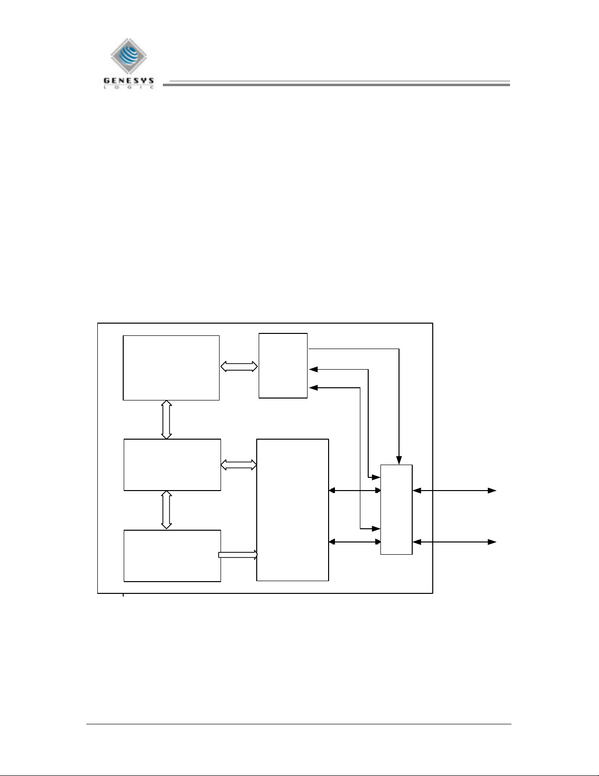
The GL603USB is a 8-bits RISC-like high performance microcontroller with a built-in 1.5Mbps SIE and
transceiver. The microcontroller features 33 instructions optimized for USB and PS/2 mouse. There are 64
bytes on-chip RAM and 2.75K x 14 program ROM incorporated into the microcontroller. Because the
GL603USB build in a clock generator circuit, it can accepts a 6 MHz ceramic resonator or a crystal as its
clock source. The clock generator can generate 12 MHz clock for micro-controller to sense mouse tracking
signal. The clock is only enabled when bit 1 of PORTCON1 register is cleared. In default firmware, it
indicates the controller is running on PS/2 mouse mode. The sampling rate of mouse tracking signal can be
up to 100 us in USB mode and 80 us in PS/2 mode. The micro-controller features 13 general purpose I/Os
(GPIOs). 8 GPIO pins build in 4 bits ADC for photo-sensor input to remove the expensive process of
matching LED and photo-sensor. Additionally, 2 GPIO pins are strong enough to drive LEDs. The other 3
GPIO pins is used for mouse buttons by default firmware. Beside the 13 GPIO pins, another 2 GPIO pins
combined with USB D+/D - functions can be used as DATA and CLK in PS/2 mode. Legacy USB cable
can be used for mouse in USB mode and an USB to PS/2 converter is required in PS/2 mode. All GPIO
ports feature low EMI emissions as a result of improved output drivers with slew -rate control.
USB Registers
&
FIFO Control
Endpoint 0
8 Bytes FIFO
Endpoint 1
8 Bytes FIFO
Select Control
Micro-
controller
USB
Interface
PS/2 CLK
PS/2 DATA
D+
D-
Figure 2-1 Block Diagram of GL603USB
D+ / PS2CLK
Mux
D- / PS2DATA
6 09/22/00
Revision 1.4
Page 7

GL603USB/GL603USB-A/GL603USB-B
3 PIN DEFINITIONS AND DESCRIPTIONS
3.1 GL603USB
Pin No. Name I/O Description
1 P1.2/LB
2 P1.3/MB I/O Port 1 bit 3/mouse middle button
3 P1.4/RB I/O Port 1 bit 4/mouse right button
4 P2.7/W2 I/O Port 2 bit 7/photo-sensor input for horizontal scroll 2
5 VCC - Voltage supply
6 XTAL2 O Ceramic resonator or crystal out
7 XTAL1 I Ceramic resonator or crystal in
8 P2.4/Z1 I/O Port 2 bit 4/photo-sensor input for vertical scroll 1
9 D+/P1.6/PS2 CLK I/O USB data+ when USBPS2 = 1
10 D-/P1.5/PS2 DATA I/O USB data- when USBPS2 = 1
11 V3.3 O 3.3V output, a 0.1uF to 1uF capacitor should be added
12 P2.5/Z2 I/O Port 2 bit 5/photo-sensor input for vertical scroll 2
13 P2.6/W1 I/O Port 2 bit 6/photo-sensor input for horizontal scroll 1
14 P1.0/LEDCTL I/O Port 1 bit 0 with LED drive capability
15 P1.1/MODESEL I/O Port 1 bit 1/mouse mode selector
16 GND - Ground
17 P2.3/Y1 I/O Port 2 bit 3/photo-sensor input for Y axis 1
18 P2.2/Y2 I/O Port 2 bit 2/photo-sensor input for Y axis 2
19 P2.1/X1 I/O Port 2 bit 1/photo-sensor input for X axis 1
20 P2.0/X2 I/O Port 2 bit 0/photo-sensor input for X axis 2
Note 1: Name or description after “/” means default function specified by Genesys Logic firmware
[1]
I/O Port 1 bit 2/mouse left button
Internal pull up 10K
Internal pull up 10K
Internal pull up 10K
Optional internal pull down from 4K ~ 32K or
no pull down resistor
Optional internal pull down from 4K ~ 32K or
no pull down resistor
Port 1 bit 6 when USBPS2 = 0. This pin is a open drain
output pin.
Port 1 bit 5 when USBPS2 = 0. This pin is a open drain
output pin.
on external circuit for this pin
Optional internal pull down from 4K ~ 32K or
no pull down resistor
Optional internal pull down from 4K ~ 32K or
no pull down resistor
Optional internal pull down from 4K ~ 32K or
no pull down resistor
Optional internal pull down from 4K ~ 32K or
no pull down resistor
Optional internal pull down from 4K ~ 32K or
no pull down resistor
Optional internal pull down from 4K ~ 32K or
no pull down resistor
Table 3-1 GL603USB Pin Definitions and Descriptions
7 09/22/00
Revision 1.4
Page 8
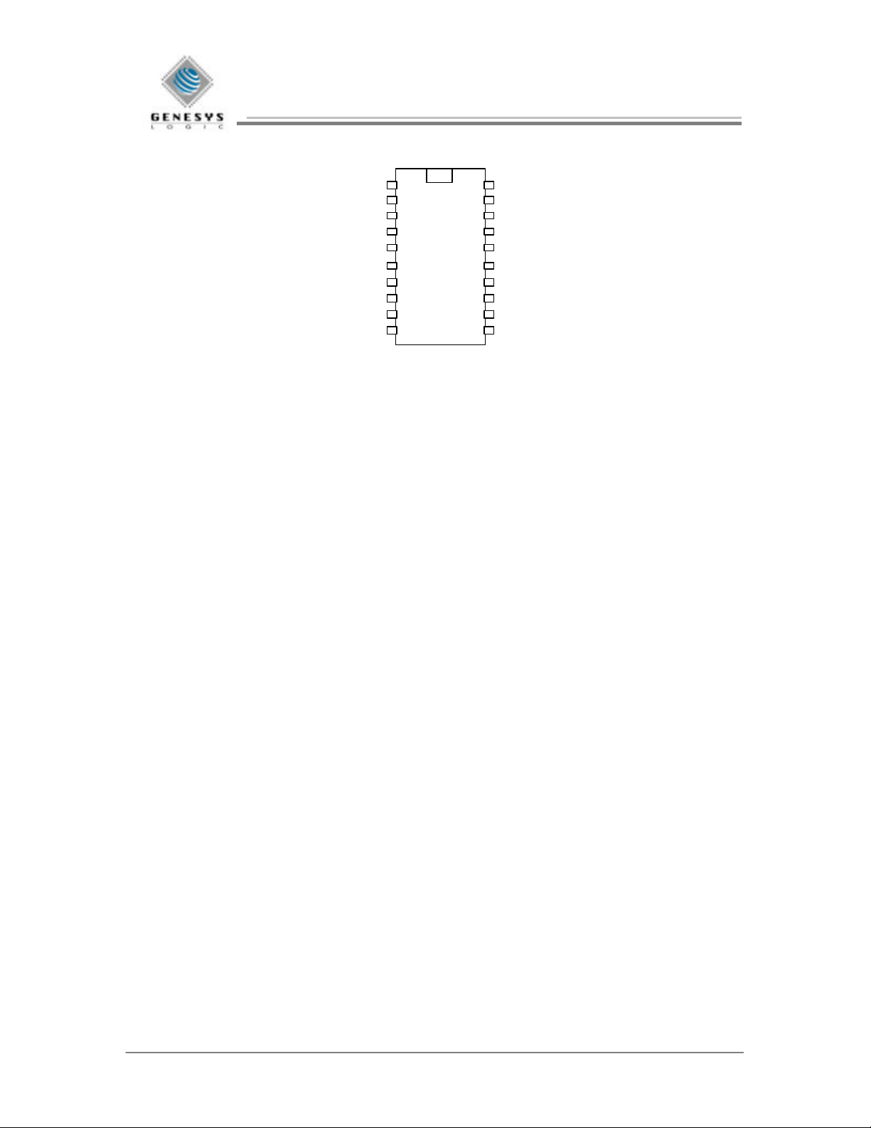
GL603USB/GL603USB-A/GL603USB-B
P1.2
P1.3
P1.4
P2.7
V
CC
XTAL2
XTAL1
P2.4
D+
D-
1 20
2 19
3 18
4 17
5 16
6 15
7 14
8 13
9 12
10 11
P2.0
P2.1
P2.2
P2.3
GND
P1.1
P1.0
P2.6
P2.5
V3.3
Figure 3-1 20-pin DIP& SOP (GL603USB)
8 09/22/00
Revision 1.4
Page 9

GL603USB/GL603USB-A/GL603USB-B
3.2 GL603USB-A
Pin No. Name I/O Description
1 P1.2/LB
2 P1.3/MB I/O Port 1 bit 3/mouse middle button
3 P1.4/RB I/O Port 1 bit 4/mouse right button
4 VCC - Voltage supply
5 XTAL2 O Ceramic resonator or crystal out
6 XTAL1 I Ceramic resonator or crystal in
7 P2.4/Z1 I/O Port 2 bit 4/photo-sensor input for vertical scroll 1
8 D+/P1.6/PS2 CLK I/O USB data+ when USBPS2 = 1
9 D-/P1.5/PS2 DATA I/O USB data- when USBPS2 = 1
10 V3.3 O 3.3V output, a 0.1uF to 1uF capacitor should be added
11 P2.5/Z2 I/O Port 2 bit 5/photo-sensor input for vertical scroll 2
12 P1.0/LEDCTL I/O Port 1 bit 0 with LED drive capability
13 P1.1/MODESEL I/O Port 1 bit 1/mouse mode selector
14 GND - Ground
15 P2.3/Y1 I/O Port 2 bit 3/photo-sensor input for Y axis 1
16 P2.2/Y2 I/O Port 2 bit 2/photo-sensor input for Y axis 2
17 P2.1/X1 I/O Port 2 bit 1/photo-sensor input for X axis 1
18 P2.0/X2 I/O Port 2 bit 0/photo-sensor input for X axis 2
[1]
I/O Port 1 bit 2/mouse lef t button
Internal pull up 10K
Internal pull up 10K
Internal pull up 10K
Optional internal pull down from 4K ~ 32K or
no pull down resistor
Port 1 bit 6 when USBPS2 = 0. This pin is a open drain
output pin.
Port 1 bit 5 when USBPS2 = 0. This pin is a open drain
output pin.
on external circuit for this pin
Optional internal pull down from 4K ~ 32K or
no pull down resistor
Optional internal pull down from 4K ~ 32K or
no pull down resistor
Optional internal pull down from 4K ~ 32K or
no pull down resistor
Optional internal pull down from 4K ~ 32K or
no pull down resistor
Optional internal pull down from 4K ~ 32K or
no pull down resistor
Table 3-2 GL603USB-A Pin Definitions and Descriptions
9 09/22/00
Revision 1.4
Page 10
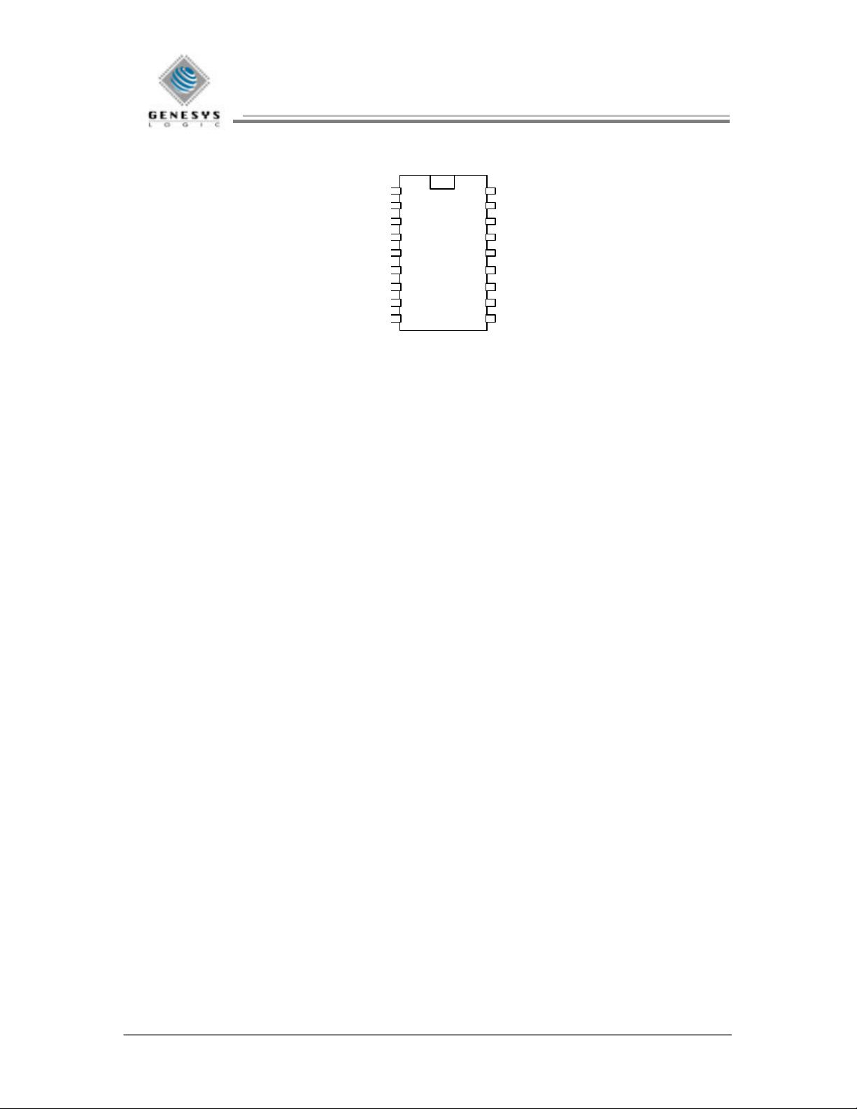
GL603USB/GL603USB-A/GL603USB-B
V3.3
9 10
P1.2
P1.3
P1.4
V
CC
XTAL2
XTAL1
P2.4
D+
D-
1 18
2 17
3 16
4 15
5 14
6 13
7 12
8 11
P2.0
P2.1
P2.2
P2.3
GND
P1.1
P1.0
P2.5
Figure 3-2 18-pin DIP & SOP (GL603USB-A)
10 09/22/00
Revision 1.4
Page 11
GL603USB/GL603USB-A/GL603USB-B
8 9
D-
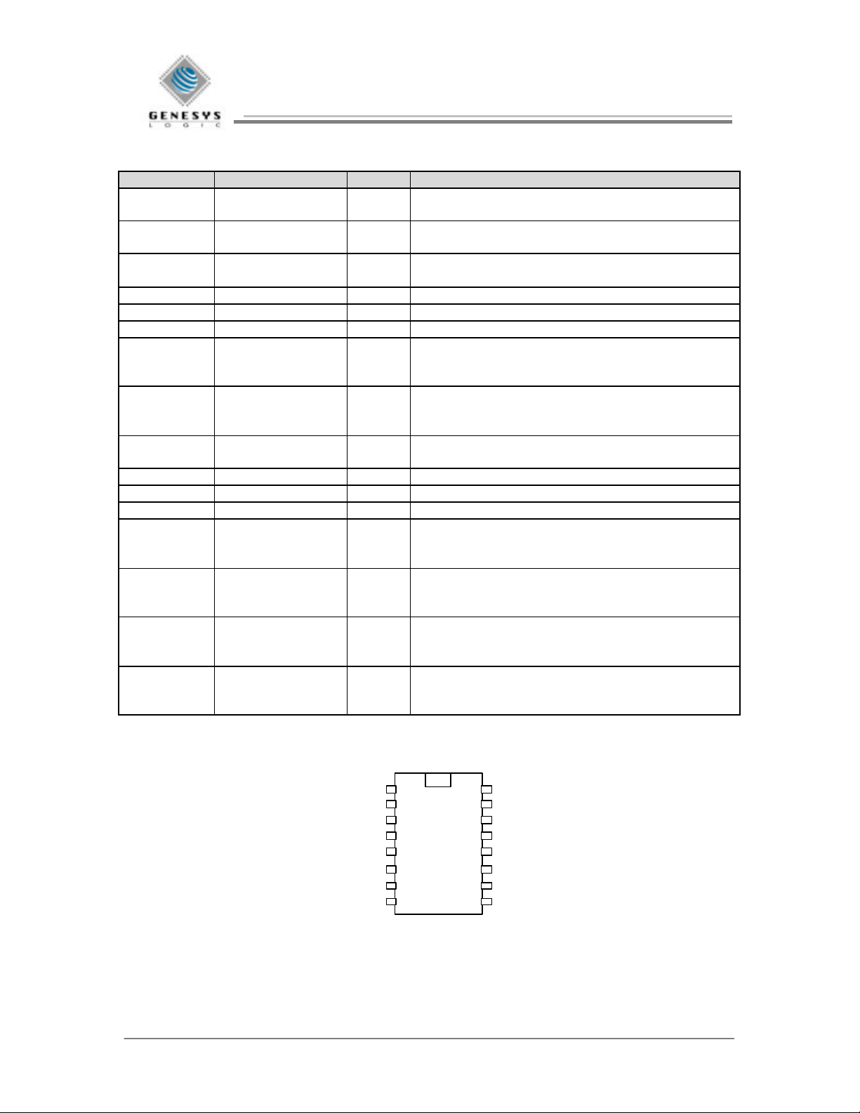
3.3 GL603USB-B
Pin No. Name I/O Description
1 P1.2/LB
2 P1.3/MB I/O Port 1 bit 3/mouse middle button
3 P1.4/RB I/O Port 1 bit 4/mouse right button
4 VCC - Voltage supply
5 XTAL2 O Ceramic resonator or crystal out
6 XTAL1 I Ceramic resonator or crystal in
7 D+/P1.6/PS2 CLK I/O USB data+ when USBPS2 = 1
8 D-/P1.5/PS2 DATA I/O USB data- when USBPS2 = 1
9 V3.3 O 3.3V output, a 0.1uF to 1uF capacitor should be added
10 P1.0/LEDCTL I/O Port 1 bit 0 with LED drive capability
11 P1.1/MODESEL I/O Port 1 bit 1/mouse mode selector
12 GND - Ground
13 P2.3/Y1 I/O Port 2 bit 3/photo-sensor input for Y axis 1
14 P2.2/Y2 I/O Port 2 bit 2/photo-sensor input for Y axis 2
15 P2.1/X1 I/O Port 2 bit 1/photo-sensor input for X axis 1
16 P2.0/X2 I/O Port 2 bit 0/photo-sensor input for X axis 1
Table 3-3 GL603USB-B Pin Definitions and Descriptions
[1]
I/O Port 1 bit 2/mouse left button
11 09/22/00
Internal pull up 10K
Internal pull up 10K
Internal pull up 10K
Port 1 bit 6 when USBPS2 = 0. This pin is a open drain
output pin.
Port 1 bit 5 when USBPS2 = 0. This pin is a open drain
output pin.
on external circuit for this pin
Optional internal pull down from 4K ~ 32K or
no pull down resistor
Optional internal pull down from 4K ~ 32K or
no pull down resistor
Optional internal pull down from 4K ~ 32K or
no pull down resistor
Optional internal pull down from 4K ~ 32K or
no pull down resistor
P1.2
P1.3
P1.4
V
CC
XTAL2
XTAL1
D+
Figure 3-3 16-pin DIP& SOP (GL603USB-B)
1 16
2 15
3 14
4 13
5 12
6 11
7 10
P2.0
P2.1
P2.2
P2.3
GND
P1.1
P1.0
V3.3
Revision 1.4
Page 12

GL603USB/GL603USB-A/GL603USB-B
4 FUNCTIONAL DESCRIPTION
The Genesys Logic GL603USB micro-controller is optimized for USB & PS/2 combo 2D/3D/4D mouse.
This USB microcontroller conforms to the low -speed (1.5Mbps) requirements of the USB Specification
version 1.1. The micro-controller is a self-contained unit with an USB SIE, an USB transceiver, an 8-bits
RISC-like microcontroller, a timer, data and program memories. It supports one USB device address and
two endpoints (include endpoint 0). The USB transceiver can be disabled in PS/2 mode and D+/D - can be
used as PS/2 CLK and DATA.
4.1 MEMORY ORGANIZATION
The memory in the microcontroller is organized into user program memory in program ROM and data
memory in SRAM space.
4.1.1 Program Memory Organization
The 12-bit Program Counter (PC) is capable of addressing 4K x 14 of program space. However, the
program space of the GL603USB is 2.75K x 14. The program memory space is divided into two functional
groups: Interrupt Vectors and program code. After a reset, the Program Counter points to location zero of
the program space. After a timer interrupt, the Program Counter points the location 0x0004 of the program
space.
After Reset
0x0000 Reset Vector
After Timer Interrupt
0x 0005
0x0AFF
Figure 4-1 Program Memory Space
4.1.2 Data Memory Organization
The data memory is partitioned into two banks that contain the General Purpose Registers, MCU Function
Registers and USB Function Registers. Bit BS is the bank select bit.
BS (STATUS<5>) = 1 → Bank 1
BS (STATUS<5>) = 0 → Bank 0
The lower locations of each Bank are reserved for MCU Function Registers and USB Function Registers.
Above the MCU Function Registers and USB Function Registers are General Pur pose Registers
implemented as SRAM. Both Bank 0 and Bank 1 contain MCU Function Registers. USB Function
Registers are located in Bank 0. Some “high use” MCU Function Registers from Bank 0 are mirrored in
Bank 1 for code reduction and quicker access.
Data Memory
Address
00h INDR 80h INDR
Data Memory
Address
→
0x0004 Timer Interrupt Vector
→
2.75K x 14 ROM
Address
12 09/22/00
Revision 1.4
Page 13
GL603USB/GL603USB-A/GL603USB-B
01h TIMER 81h PSCON
02h PCL 82h PCL
03h STATUS 83h STATUS
04h INDAR 84h INDAR
05h 85h
06h PORT1 86h PORT1CON
07h PORT2 87h PORT2CON
08h 88h
09h 89h
0Ah PCHBUF 8Ah PCHBUF
0Bh INTEN 8Bh INTEN
0Ch 8Ch
0Dh PHVAL 8Dh
0Eh PHSEL 8Eh
0Fh DMODE 8Fh
10h DEVCTL 10h
11h MODSEL 11h
12h EVTFLG 12h
13h DEVADR 13h
14h FFCNT0 14h
15h FFCNT1 15h
16h FFCTL 16h
17h FFDAT0 17h
18h FFDAT1 18h
19h EP0RXST 19h
1Ah
1Fh
20h
5Fh
60h
7Fh
Bank 0 Bank 1
4.2 USB FUNCTION REGISTERS
Address Name Function
10h DEVCTL Device control register
11h MODSEL Mode select register
12h EVTFLG Event flag register
13h DEVADR USB device address register
14h FFCNT0 Byte count buffer for endpoint 0
General
Purpose
Registers
(64 bytes)
FFh
Figure 4-2 Data Memory Space
13 09/22/00
Revision 1.4
Page 14

GL603USB/GL603USB-A/GL603USB-B
15h FFCNT1 Byte count buffer for endpoint 1
16h FFCTL FIFO control register
17h FFDAT0 Endpoint 0 FIFO port
18h FFDAT1 Endpoint 1 FIFO port
19h EP0RXST Endpoint 0 receiving status register
Table 4-1 USB Function Register Summary
DEVCTL (Address 10h, Device control register)
[1]
R/W
R/W R/W R/W R/W R/W
TXSE0 EP0STL EP1STL WAKE WKDIS PWRDN
TXSE0: Set and clear transmitting SE0 bit
1: Set transmitting SE0
0: Clear transmitting SE0
EP0STL: Endpoint 0 stall bit. This bit will be cleared automatically by hardware when SETUP packet is
received
1: Endpoint 0 will respond with a STALL to a valid transaction except SETUP
0: Endpoint 0 will not respond with a STALL to a valid transaction
EP1STL: Endpoint 1 stall bit
1: Endpoint 1 will respond with a STALL to a valid transaction
0: Endpoint 1 will not respond with a STALL to a valid transaction
WAKE: Wake-up bit
1: Set this bit to wake up host controller by placing USB bus into K state
0: Clear this bit to force USB bus leave K state
WKDIS: Wake-up disable bit. The WAKE bit has no effect if WKDIS bit is set to 1.
1: Disable remote wake-up capability
0: Enable remote wake-up capability
PWRDN: Power -down mode bit. Writing 1 to this bit will enter power-down mode
If USB suspend is detected, firmware can set this bit to enter power -down mode. In power-down
mode, crystal/resonator will stop. The PWRDN bit will be cleared automatically by hardware and
crystal/resonator will restart when the internal RC timer timeout (about 300ms for mask, 500ms
for OTP). Firmware should check buttons and photo position encoders of the mouse. If mouse
status is not changed, Firmware should set the PWRDN bit to enter power down mode again.
Power consumption in suspend mode depends on how much time the firmware checking mouse
status changed. Hardware will also clear PWRDN bit automatically when USB D+ or D- is
toggled.
0: Normal mode, not power-down
Value on POR: “1 - 0 - 0 0 0 0”
[2]
Note 1: “R/W” means readable and writable bit. All reserved fields should not be changed by firmware.
Note 2: “-“ means unimplemented read as 0
MODSEL (Address 11h, Mode select register)
R/W
USBPS2
USBPS2: USB or PS/2 mode selector bit
1: USB mode, enable SIE
0: PS/2 mode, disable SIE
Value on POR: “- - - 0 - - - -”
EVTFLG (Address 12h, Event flag register)
R/W1C
[1]
R/W1C R/W1C R/W1C R/W1C
RESUME SUSPD EP1TX EP0TX EP0RX
RESUME: Global resume bit
1: Global resume (USB D+/D - toggle) was detected
14 09/22/00
Revision 1.4
Page 15

GL603USB/GL603USB-A/GL603USB-B
0: Global resume was not detected
SUSPD: Global suspend bit
1: Global suspend (USB idle more than 3ms) was detected
0: Global suspend was not detected
EP1TX: Endpoint 1 transmitting status bit
1: Data has been sent from endpoint 1
0: Data has not been sent from endpoint 1
EP0TX: Endpoint 0 transmitting status bit
1: Data has been sent from endpoint 0
0: Data has not been sent from endpoint 0
EP0RX: Endpoint 0 receiving status bit
1: Data has been received by endpoint 0
0: Data has not been received by endpoint 0
Note 1: “R/W1C” means read-only and write “1” to clear bit
DEVADR (Address 13h, USB device address register)
R/W R/W R/W R/W R/W R/W R/W
DADR6 DADR5 DADR4 DADR3 DADR2 DADR1 DADR0
Write this register to set the USB device address
Value on POR: “- 0 0 0 0 0 0 0”
FFCNT0 (Address 14h, Byte count buffer for endpoint 0)
[1]
R/O
R/O R/O R/O R/W R/W R/W R/W
RXCNT3 RXCNT2 RXCNT1 RXCNT0 TXCNT3 TXCNT2 TXCNT1 TXCNT0
RXCNT[3:0]: Number of bytes received by endpoint 0 OUT transaction
TXCNT[3:0]: Number of bytes to be sent by endpoint 0 IN transaction
Note 1: “R/O” means read-only bit. Writing this bit is no effect.
FFCNT1 (Address 15h, Byte count buffer for endpoint 1)
R/W R/W R/W R/W
TXCNT3 TXCNT2 TXCNT1 TXCNT0
TXCNT[3:0]: Number of bytes to be sent by endpoint 1 IN transaction
Value on POR: “- - - - x x x x”
FFCTL (Address 16h, FIFO control register)
W/O
[1]
R/W R/W R/W W/O R/W R/W
FFRST1 TXSEQ1 TXOE1 RXDIS0 FFRST0 TXSEQ0 TXOE0
FFRST1: Reset endpoint 1 FIFO read/write pointer
Write “1” to this bit will reset endpoint 1 FIFO read/write pointer. Data in endpoint 1 FIFO remain
unchanged. Before data are written into endpoint 1 FIFO, FFRST1 should be written first.
TXSEQ1: Endpoint 1 transmitting sequence bit
1: Transmitting data use DATA 1 as PID
0: Transmitting data use DATA 0 as PID
TXOE1: Endpoint 1 FIFO data ready bit
1: Endpoint 1 FIFO data are ready to be transmitted. Data will be transmitted when a valid IN
token is received. This bit is automatically cleared by hardware after the transaction complete
(ACK is received).
0: Endpoint 1 FIFO data are not ready to be transmitted. Endpoint 1 will respond with a NAK to a
valid IN transaction.
RXDIS0: Endpoint 0 receiving not available bit
1: Endpoint 0 FIFO is not available. The received data cannot be pushed into FIFO. The USB
controller will respond with a NAK to a valid OUT transaction. This bit is set by hardware when
15 09/22/00
Revision 1.4
Page 16

GL603USB/GL603USB-A/GL603USB-B
endpoint 0 data is received (both SETUP and OUT transaction) and should be cleared by firmware
after data is read from FIFO.
0: Endpoint 0 FIFO is available for data receiving
FFRST0: Reset endpoint 0 FIFO read/write pointer
Write “1” to this bit will reset endpoint 0 FIFO read/write pointer. Data in endpoint 0 FIFO remain
unchanged. Before data are written into endpoint 0 FIFO, FFRST0 should be written first.
TXSEQ0: Endpoint 0 transmitting sequence bit
1: Transmitting data use DATA 1 as PID
0: Transmitting data use DATA 0 as PID
TXOE0: Endpoint 0 FIFO data ready bit
1: Endpoint 0 FIFO data are ready to be transmitted. Data will be transmitted when a valid IN
token is received. This bit is automatically cleared by hardware after the transaction complete
(ACK is received).
0: Endpoint 0 FIFO data are not ready to be transmitted and respond with a NAK to a valid IN
transaction.
Value on POR: “- 0 0 0 0 0 0 0”
Note 1: “W/O” means write-only bit. 0 will be returned when reading this bit
FFDAT0 (Address 17h, Endpoint 0 FIFO port)
R/W R/W R/W R/W R/W R/W R/W R/W
FFDAT7 FFDAT6 FFDAT5 FFDAT4 FFDAT3 FFDAT2 FFDAT1 FFDAT0
Endpoint 0 FIFO data port
Endpoint 0 FIFO is a 8 bytes FIFO. Firmware can read/write this port 8 times to get/put the FIFO
data.
Value on POR: “x x x x x x x x”
FFDAT1 (Address 18h, Endpoint 1 FIFO port)
R/W R/W R/W R/W R/W R/W R/W R/W
FFDAT7 FFDAT6 FFDAT5 FFDAT4 FFDAT3 FFDAT2 FFDAT1 FFDAT0
Endpoint 1 FIFO port
Endpoint 1 FIFO is 8 bytes FIFO. Firmware can read this port 8 times to get the FIFO data.
Value on POR: “x x x x x x x x”
EP0RXST (Address 19h, Endpoint 0 receiving status register)
R/O R/O R/O R/O
RXST3 RXST2 RXST1 RXST0
RXST[3:0]: If EP0RX is set, then there’s a complete transaction. RXST[3:0] indicate the packet received.
Bit Value Packet received
1001 SETUP token with DATA0 packet
0101 OUT token with DATA0 packet
0110 OUT token with DATA1 packet
Value on POR: “- - - - x x x x”
4.3 MCU FUNCTION REGISTERS
Address Name Function
00h INDR Addressing this location will use the content of INDAR to address data
memory (not a physical address)
01h TIMER Timer register
02h PCL Program Counter’s low byte
03h STATUS Status register
04h INDAR Indirect address register
16 09/22/00
Revision 1.4
Page 17

GL603USB/GL603USB-A/GL603USB-B
06h PORT1 Port 1 data register
07h PORT2 Port 2 data register
0Ah PCHBUF Write buffer of Program Counter’s bi t 10-8
0Bh INTEN Interrupt enable register
0Dh PHVAL Photo-sensor value register
0Eh PHSEL Photo-sensor input select register
0Fh DMODE Photo-sensor input mode register
80h INDR Addressing this location will use the content of INDAR to address data
memory (not a physical address)
81h PSCON Prescaler control register
82h PCL Program Counter’s low byte
83h STATUS Status register
84h INDAR Indirect address register
86h PORT1CON Port 1 direction control register
87h PORT2CON Port 2 direction control register
8Ah PCHBUF Write buffer of Program Counter’s bit 10-8
8Bh INTEN Interrupt enable register
Table 4-2 MCU Function Register Summary
INDR (Address 00h/80h)
INDR is not a physical register. Addressing INDR register will cause indirect addressing. Any instruction
using the INDF register actually accesses the register pointed by the INDAR register.The indirect
addressing method only can be used for general purpose registers.
TIMER (Address 01h, Timer register)
R/W R/W R/W R/W R/W R/W R/W R/W
TIMER7 TIMER6 TIMER5 TIMER4 TIMER3 TIMER2 TIMER1 TIMER0
The timer starts to count up after power on reset. The TMROF bit at INTEN register will be set when the
TIMER register overflows from FFh to 00h. If both TMROEN and GIE bits at INTEN register are set, an
interrupt will be generated when TIMER register overflows.
Value on POR: “0 0 0 0 0 0 0 0”
PCL (Address 02h/82h, Program Counter’s low byte)
R/W R/W R/W R/W R/W R/W R/W R/W
PCL7 PCL6 PCL5 PCL4 PCL3 PCL2 PCL1 PCL0
The Program Counter (PC) is 11-bit wide. The low byte comes from the PCL register, which is a readable
and writable register. The high byte is not directly readable or writable and comes from PCHBUF. The
GL603USB has a 4 level deep x 11-bit wide hardware stake. The stake space is not part of either program
or data space and the stack pointer is not readable or writable. The PC is pushed onto the stack when a
CALL instruction is executed or an interrupt causes a branch. The stack is poped in the event of a RETIA,
RETI or a RET instruction execution. PCHBUF is not affected by a push or pop operation.
When write to PCL command executed, all 3 bits of PCHBUF will be loaded to PC because PCL is only a
8 bits register.
Value on POR: “0 0 0 0 0 0 0 0”
Status (Address 03h, Status register)
R/W R/W R/W R/W
BS ZO HC CA
BS: Bank Select. Because only 7 bits (bit 0~bit 6) operand implied by instruction for register address, this
bit is used as address bit 7 when register access.
1: Bank 1 (80h-FFh)
17 09/22/00
Revision 1.4
Page 18

GL603USB/GL603USB-A/GL603USB-B
0: Bank 0 (00h-7Fh)
ZO: Zero bit
1: The result of an arithmetic or logic operation is zero
0: The result of an arithmetic or logic operation is not zero
HC: Half Carry/Borrow bit
1: Carry or not borrow from the 4th low order bit
0: Borrow or not carry from the 4th low order bit
CA: Carry/Borrow bit
1: Carry or not borrow from the most significant bit
0: Borrow or not carry from the most significant bit
Value on POR: “- - 0 - - 0 0 0”
INDAR: (Address 04h/84h, Indirect address register)
R/W R/W R/W R/W R/W R/W R/W R/W
INDAR7 INDAR6 INDAR5 INDAR4 INDAR3 INDAR2 INDAR1 INDAR0
Any instruction using the INDF register actually accesses the register pointed by the INDAR register.
Value on POR: “x x x x x x x x”
[1]
Note 1: “x” means unknown
PORT1 (Address 06h, Port 1 data register)
R/W R/W R/W R/W R/W R/W R/W
PORT1.6 PORT1.5 PORT1.4 PORT1.3 PORT1.2 PORT1.1 PORT1.0
PORT1 is a 7-bits latch for Port 1.0~Port 1.6. Reading the PORT1 register gets the status of the pins.
Writing to it will write to the port latch. All write operations are read-modify-write operations.
PORT1CON is used to enable/disable every bits of the port latch.
Port 1.5 and Port 1.6 are combined with USB D+ and D- pins and can be used only when USBPS2 bit at
MODSEL is cleared. These 2 I/O pins are open drain output and should be external pulled up at PS/2 mode.
Value on POR: “- x x x x x x x”
PORT2 (Address 07h, Port 2 data register)
R/W R/W R/W R/W R/W R/W R/W R/W
PORT2.7 PORT2.6 PORT2.5 PORT2.4 PORT2.3 PORT2.2 PORT2.1 PORT2.0
PORT2 is an 8-bits latch for Port 2.0~Port 2.7. Reading the PORT2 register reads the status of the pins.
Writing to it will write to the port latch. All write operations are read-modify-write operations.
PORT2CON is used to enable/disable every bits of the port latch.
Value on POR: “x x x x x x x x”
PCHBUF (Address 0Ah/8Ah, Write buffer of Program Counter’s bit 11-8)
R/W R/W R/W R/W
PCHBUF3 PCHBUF2 PCHBUF1 PCHBUF0
Write buffer for upper 4-bit of Program Counter. The upper byte of Program Counter is not directly
accessible. PCHBUF is a holding register for the PC[11:8] that are transferred to the upper byte of the
Program Counter when branch occur. Please see PCL register to get more detail information.
Value on POR: “- - - - 0 0 0 0”
INTEN (Address 0Bh/8Bh, Interrupt enable register)
R/W R/W R/W
GIE TMROEN TMROF
GIE: Global interrupt enable bit
1: Enable all interrupts
0: Disable all interrupts
TMROEN: Timer overflow interrupt enable bit
1: Enable timer interrupt
18 09/22/00
Revision 1.4
Page 19

GL603USB/GL603USB-A/GL603USB-B
0: Disable timer interrupt
TMROF: Timer overflow interrupt flag bit. This bit should be cleared to ‘0’ by firmware after it is set by
hardware.
1: Timer register has overflowed
0: Timer register did not overflow
Value on POR: “0 - 0 - - 0 - -“
PHVAL (Address 0Dh, Photo-sensor value register)
R/O R/O R/O R/O
PHVAL3 PHVAL2 PHVAL1 PHVAL0
PHVAL[3:0]: the 8 channel, 4 bits analog-to-digital converter data. The ADC input is select by PHSEL
register from Port 2.0~Port 2.7
Bit Value Analog value
0000 0 V - 5/16 V
0001 5/16 V - 5/8 V
0010 5/8 V - 15/16 V
0011 15/16 V - 5/4 V
0100 5/4 V - 25/16 V
0101 25/16 V - 15/8 V
0110 15/8 V - 35/16 V
0111 35/16 V - 5/2 V
1000 5/2 V - 45/16 V
1001 45/16 V - 25/8 V
1010 25/8 V - 55/16 V
1011 55/16 V - 15/4 V
1100 15/4 V - 65/16 V
1101 65/16 V - 75/16 V
1110 75/16 V - 5V
1111 5V
Value on POR: “- - - - x x x x”
PHSEL (Address 0Eh, Photo-sensor analog input select register)
R/W R/W R/W
PHSEL2 PHSEL1 PHSEL0
PHSEL[2:0]: The selection register for 8 channel 4 bits, ADC.
Bit Value Source pin of the ADC
000 PORT2.0
001 PORT2.1
010 PORT2.2
011 PORT2.3
100 PORT2.4
101 PORT2.5
110 PORT2.6
111 PORT2.7
Value on POR: “- - - - - x x x”
DMODE (Address 0Fh, Photo-sensor input mode register)
R/W R/W R/W R/W R/W R/W R/W R/W
DMODE7 DMODE6 DMODE5 DMODE4 DMODE3 DMODE2 DMODE1 DMODE0
DMODE[7:0]: Individual enabler for Port 2.7~Port 2.0 input buffer.
1: Indicate the corresponding pin on Port 2 can be used in input mode. This pin can be selected
with PHSEL and firmware can get its state from PHVAL also.
19 09/22/00
Revision 1.4
Page 20

GL603USB/GL603USB-A/GL603USB-B
0: Indicate the corresponding pin on Port 2 cannot be used in input mode. But even firmware
cannot read this pin directly from Port 2 directly, this pin can be selected with PHSEL and
firmware can get its state from PHVAL also.
Value on POR: “0 0 0 0 0 0 0 0”
PSCON (Address 81h, Prescaler control register)
R/W R/W R/W R/W
PSDIS PS2 PS1 PS0
PSDIS: Prescaler disable bit
1: Set prescaler disable
0: Set prescaler enable
PS[2:0]: Prescaler rate select bits. These bits are used to control timer speed. The following table means
that how many instruction cycles the TIMER register should be added by 1 when PSDIS = 0.
Bit Value Timer Rate
(PSDIS = 0)
000 1:2
001 1:4
010 1:8
011 1:16
100 1:32
101 1:64
110 1:128
111 1:256
Value on POR: “- - - - 1 1 1 1”
PORT1CON (Address 86h, Port 1 direction control register)
R/W R/W R/W R/W R/W R/W R/W
P1CON6 P1CON5 P1CON4 P1CON3 P1CON2 P1CON1 P1CON0
There is a data direction control bit to match every pin of Port 1. The direction control bits can configure
these pins as output or input. Setting a PORT1CON register bit put the corresponding output driver in a hi impedance mode. Clearing a bit in the PORT1CON register puts the contents of the output latch on the
selected pin.
Except to control PORT1.1 output driver, a special function is applied to P1CON1. Clock generator in
GL603USB can be enabled only when P1CON1 is cleared. When a 6 MHz crystal or resonator is used and
P1CON1 is set, GL603USB cannot running on 12 MHz, even if clock generator is enabled by code option.
Value on POR: “- 1 1 1 1 1 1 1”
PORT2CON (Address 87h, Port 2 direction control register)
R/W R/W R/W R/W R/W R/W R/W R/W
P2CON7 P2CON6 P2CON5 P2CON4 P2CON3 P2CON2 P2CON1 P2CON0
There is a data direction control bit to match every pin of Port 2. The direction contr ol bits can configure
these pins as output or input. Setting a PORT2CON register bit put the corresponding output driver in a hiimpedance mode. Clearing a bit in the PORT2CON register puts the contents of the output latch on the
selected pin.
Value on POR: “1 1 1 1 1 1 1 1”
4.4 FULL-RANGE DETECTION AND ANALOG -TO-DIGITAL CONVERTER
20 09/22/00
Revision 1.4
Page 21

GL603USB/GL603USB-A/GL603USB-B
The GL603USB provides the unique “Full-Range Detection” ability. Over 95% of PC mouse market adopts
photo-sensor system to detect the mechanical movement of the roller inside the mouse. Because the
sensors may have varied characteristic on their output DC voltage level and output moving range, the
mouse manufacturers can’t avoid the expensive process of matching LED and photo-sensor. By providing
those photo-input pins with full-range detection function, the mouse makers can ignore the range difference
between those sensors, so the manufacturing procedure is simple and a huge cost is saved on the
manufacturing line.
By detecting the output signal came from the sensors, Genesys Logic’s patented algorithm could learn the
tiny difference of every signal and automatically adjust the threshold for the sensors without any side effect.
This new outstanding design can help the manufacturers decrease their inconvenience on mass -production
line and cut their human and mechanical cost tremendously.
There’s a 4-bit Analog-to-Digital Converter (ADC) module in the GL603USB. The input signal of ADC
can be connected to Port 2.0 ~ Port 2.7. When these I/O pins is used for analog input, the corresponding
bits in DMODE register should be set to 0 to disable input buffer of Port 2. This can save power consumed
by the pad of Port 2. The PHSEL register is used to select which input connected to the ADC and the
PHVAL register is used to store the digital value converted by the ADC. The Genesys Logic’s proprietary
algorithm can detect any analog waveform from photo-sensor with amplitude larger than 1V. The ADC is a
high-speed converter. It takes less than 500ns to complete the conversion. Because GL603USB is running
at 3 MIPS for USB low speed application, only two dummy instructions should be added between write
PHSEL to read PHVAL.
4.5 CLOCK GENERATOR
The GL603USB build in a clock generator circuit to generate the 12 MHz clock for micro-controller and 6
MHz clock for USB engine use. The clock generator is enabled only when bit 1 of PORTCON1 is cleared.
With the clock generator, we can only use a 6 MHz ceramic resonator or crystal to reduce EMI. The clock
generator can be disabled by code option. When the clock generator is disabled, the 6 MHz clock is used by
micro-controller and USB engine directly. When 12 MHz resonator or crystal is used, the 12 MHz clock is
directly used by micro-controller and divided by 2 before used by USB engine. The clock division can be
programmed by another code option when 12 MHz ceramic resonator or crystal is used.
4.6 GENERAL PURPOSE I/O PORTS
Interface with peripherals is conducted via up to 15 GPIO signals. These 15 signals are divided into two
ports: Port 1 and Port 2. Port 1 contains seven lines (PORT1.0-PORT1.6) and Port 2 contains eight lines
(PORT2.0-PORT2.7). The Port 1 data register is located at data memory address 06h while the Port 2 data
register is located at data memory address 07h.
Port 2 is a low current port with analog input capability suitable for connecting photo-sensor. Port 1 is a
high current port capable of LED drive. PORT1.5 and PORT1.6 (which is combined with USB D+/D -) are
open drain output. Therefore, they can only drive low at output mode and external pulled up resistor should
be added. This is enough for PS/2 CLK and DATA. Except these 2 GPIO lines, each GPIO line may
include an internal pull-up or pull-down resistor. Port 2’s internal pull-down resistor value can be
programmed by option-code. Each output drive has slew -rate control to reduce EMI. Please see the
following table for details.
Driving capability Pull-up resistor Pull-down resistor
PORT1.0 20 mA
PORT1.1 20 mA
PORT1.2 4 mA
10KΩ
21 09/22/00
Revision 1.4
Page 22

GL603USB/GL603USB-A/GL603USB-B
PORT1.3 4 mA
PORT1.4 4 mA
PORT1.5 4 mA (open drain)
PORT1.6 4 mA (open drain)
PORT2.0 4 mA
PORT2.1 4 mA
PORT2.2 4 mA
PORT2.3 4 mA
PORT2.4 4 mA
PORT2.5 4 mA
PORT2.6 4 mA
PORT2.7 4 mA
Note 1: The pull-down resistor can be configured as 4KΩ, 8KΩ, 16KΩ or 32KΩ by option-code.
Table 4-3 General Purpose I/O Port Summary
10KΩ
10KΩ
4KΩ/8KΩ/16KΩ/32KΩ
4KΩ/8KΩ/16KΩ/32KΩ
4KΩ/8KΩ/16KΩ/32KΩ
4KΩ/8KΩ/16KΩ/32KΩ
4KΩ/8KΩ/16KΩ/32KΩ
4KΩ/8KΩ/16KΩ/32KΩ
4KΩ/8KΩ/16KΩ/32KΩ
4KΩ/8KΩ/16KΩ/32KΩ
[1]
4.7 TIMER INTERRUPT
The Timer Interrupt is generated when the TIMER register overflows from FFh to 00h. This overflow sets
bit TMROF (INTEN<2>). The interrupt can be masked by clearing bit TMROEN (INTEN<5>). Bit
TMROF must be cleared in software by the Timer module interrupt service routine otherwise the Timer
Interrupt will not be generated again. If prescaler is disabled, the timer register will increase every
instruction cycle. If prescaler is enabled, its increment cycle depends on PS0~PS2 bits in PSCON register.
4.8 USB ENGINE
The USB module contains three functional blocks: a 3.3-volt regulator, a low-speed USB transceiver, and
the Serial Interface Engine (SIE). The USB module is only enabled under USB mode. While the mouse is
working under PS/2 mode, the USB module is disabled and D+/D - working as open drain GPIO pins. The
following details the function of the regulator, transceiver, and SIE.
4.8.1 Voltage Regulator
The USB data lines are required by the USB specification to have a maximum output voltage between 2.8V
and 3.6V. Because the GL603USB is a low speed USB devi ce, the D- lines also are required to have an
external 1.5-kΩ pull-up resistor connected between a data line and a voltage source between 3.0 V and 3.6
V. Since the power provided by the USB cable is specified to be between 4.4V and 5.0V, an on-chip
regulator is used to drop the voltage to the appropriate level for sourcing the USB transceiver and external
pull-up resistor. An output pin driven by the regulator is provided to source the 1.5-kΩ external resistor.
4.8.2 USB Transceiver
The USB transceiver provides the physical interface to the USB D+ and D- data lines. The transceiver is
composed of two parts: an output driver circuit and a receiver.
The USB transceiver uses a differential output driver to driver the USB data signal onto the USB cable. The
static output swing of the driver in its low state is below the V
its high state is above the VOH of 2.8V with 15-kΩ load to ground. The output swings between the
differential high and low state are well balanced to mini mize signal skew. Slew rate control on the driver is
used to minimize the radiated noise and cross talk. The driver’s outputs support 3-state operation to achieve
bi-directional half-duplex operation. The driver can tolerate a voltage on the signal pins of –0.5V to 3.8V
with respect to local ground reference without damage.
of 0.3V with 1.5-kΩ load to 3.6V and in
OL
22 09/22/00
Revision 1.4
Page 23

GL603USB/GL603USB-A/GL603USB-B
The rise and fall time of the signals on this cable are greater than 75ns to keep RFI (radio frequency
interference) emissions under FCC (Federal Communications Commission) class B limits and less than
300ns to limit timing delays, signaling skews, and distortions. The driver reaches the specified static signal
levels with smooth rise and fall times, and minimal reflections and ringing when driving the cable. This
driver is used only on segments between low -speed devices and the ports to which they are connected.
USB data transmission is done with differential signals. A differential input receiver is used to accept the
USB data signal. A differential 1 on the bus is represented by D+ being at least 200mV more positive than
D- as seen at the receiver, and a differential 0 is represented by D- being at least 200mV more positive than
D+ as seen at the receiver. The signal cross over point must be between 1.3V and 2.0V.
The receiver featur es an input sensitivity of 200mV when both differential data inputs are in the range of
0.8V and 2.5V with respect to the local ground reference. This is called the common mode input voltage
range. Proper data reception also is achieved when the differenti al data lines are outside the common mode
range. The receiver can tolerate static input voltage between –0.5V to 3.8V with respect to its local ground
reference without damage. In addition to the differential receiver, there is a single-ended receiver for each
of the two data lines.
1.0
0.8
0.6
0.4
0.2
Minimum Differential Sensitivity (volts)
0.0
0.0 0.2 0.4 0.6 0.8 1.0 1.2 1.4 1.6 1.8 2.0 2.2 2.4 2.6 2.8 3.0 3.2
Common Mode Input Voltage (volts)
Figure 4-3 Differential Input Sensitivity over Entire Common Mode Range
The data receivers for all types of devices must be able to properly decode the differential data in the
presence of jitter. The more of the bit time that any data edge can occupy and still be decoded, the more
reliable the data transfer will be. Data receivers are required to decode differential data transitions that
occur in a window plus and minus a nominal quarter bit time from the nominal (centered) data edge
position. Jitter will be caused by the delay mismatches and by mismatches in the source and destination
data rates (frequencies).
23 09/22/00
Revision 1.4
Page 24

GL603USB/GL603USB-A/GL603USB-B
PERIOD
10%
90%
FtR
10%
90%
T
Differential
Data Lines
TJR TJR1 T JR2
Consecutive
Transitions
N * TPERIOD + TJR1
Paired
Transitions
N * TPERIOD + TJR2
Figure 4-4 Receiver Jitter Tolerance
The source of data can have some variation (jitter) in the timing of edges of the data transmitted. The time
between any set of data transitions is N*T
transitions and T
is defined as the actual period of the data rate. The data jitter is measured with the
Period
± jitter time, where N is the number of bits between the
Period
same capacitive load used for maximum rise and fall times and is measured at the crossover points of the
data lines.
For low -speed transmissions, the jitter time for any consecutive differential data transitions must be within
±25ns and within ±10ns for any set of paired differential data transitions. These jitter numbers include
timing variations due to differential buffer delay, rise/fall time mismatches, internal clock source jitter,
noise and other random effects.
The output rise time and fall time are measured between 10% and 90% of the signal. Edge transition time
for the rising and falling edges of low -speed signals is 75ns (minimum) into a capacitive load (CL) of 50pF
and 300ns (maximum) into a capacitive load of 350pF. The rising and falling edges should be transitioning
(monotonic) smoothly when driving the cable to avoid excessive EMI.
CL
CL
4.8.3 Serial Interface Engine (SIE)
The SIE manages data movement between the CPU and the transceiver. The SIE handles both transmit and
receive operations on the USB. It contains the logic used to manipulate the transceiver and the endpoint
registers.
24 09/22/00
Rise Time
Differential
Data Lines
Low Speed: 75ns at CL = 50pF, 300ns at C L = 350pFFull Speed: 4 to 20ns at CL = 50pF
Figure 4-5 Data Signal Rise and Fall Time
Fall Time
t
Revision 1.4
Page 25

GL603USB/GL603USB-A/GL603USB-B
The byte count buffer is loaded from TXCNT(TXCTL0<3~0>) during endpoint 0 transmit operations. This
same buffer is used for receive transactions to count the number of bytes received at endpoint 0 and, upon
the end of transaction, transfer the value to RXCNT(RXCTL0<3~0>).
When transmitting, the SIE handles parallel -to-serial conversion, CRC generation, NRZI encoding, and bit
stuffing. When receiving, the SIE handles sync detection, packet identification, end-of-packet detection, bit
(un)stuffing, NRZI decoding, CRC validation, and serial -to-parallel conversion. Errors detected by the SIE
include bad CRC, timeout while waiting for EOP, and bit stuffing violations.
All USB devices are required to have an endpoint 0 that is used to initialize and manipulate the device.
Endpoint 0 provides access to the device’s configuration information and allows generic USB status and
control accesses. Endpoint 0 can receive and transmit data. Both receive and transmit data share the same
8-byte Endpoint 0 FIFO, FFDAT0. Received data may overwrite the data previously in the FIFO.
Endpoint 1 is of transmit only. This endpoint is used to transmit HID report data to host.
4.9 INSTRUCTION SET SUMMARY
4.9.1 Operand Field Descriptions
Field Description
r Register address
A Accumulator
i Immediate data
b Bit address within a 8-bit register
4.9.2 Instruction Set
Mnemonic,
Operands
Arithmetic Operations
ADDAR r, A Add r and A, r <- r + A 1 CA, HC, ZO
ADDAR A, r Add A and r, A <- A + r 1 CA, HC, ZO
ADDAI i Add A and i, A <- A + i 1 CA, HC, ZO
INCR r Increment r, r <- r +1 1 ZO
INCR A, r Increment r, A <- r + 1 1 ZO
INCRSZ r Increment r, r <- r +1, skip if (r = 0) 1 or 2
INCRSZ A, r Increment r, A <- r +1, skip if (A = 0) 1 or 2
SUBAR r, A Subtract A from r, r <- r - A 1 CA, HC, ZO
SUBAR A, r Subtract A from r, A <- r - A 1 CA, HC, ZO
SUBIA i Subtract A from i, A <- i - A 1 CA, HC, ZO
DECR r Decrement r, r <- r -1 1 ZO
DECR A, r Decrement r, A <- r -1 1 ZO
DECRSZ r Decrement r, r <- r-1, skip if (r = 0) 1 or 2
DECRSZ A, r Decrement r, A <- r – 1, skip if (A = 0) 1 or 2
CLRR r Clear r, r <- 0 1 ZO
CLRA Clear A, A <- 0 1 ZO
NOP No operation 1
Logical Operations
Description Cycles Flags
Affected
25 09/22/00
Revision 1.4
Page 26

GL603USB/GL603USB-A/GL603USB-B
ANDAR r, A And r and A, r <- r & A 1 ZO
ANDAR A, r And A and r, A <- A & r 1 ZO
ANDAI i And A and i, A <- A & i 1 ZO
CMPR r Complement r, r <- r ^ FF 1 ZO
CMPR A, r Complement r, A <- r ^ FF 1 ZO
ORAR r, A Inclusive OR r with A, r <- r | A 1 ZO
ORAR A, r Inclusive OR A with r, A <- A | r 1 ZO
ORIA i Inclusive OR i with A, A <- A | i 1 ZO
XORAR r, A Exclusive OR r with A, r <- r ^ A 1 ZO
XORAR A, r Exclusive OR A with r, A <- A ^ r 1 ZO
XORIA i Exclusive OR i with A, A <- A ^ i 1 ZO
Bit-wise Operations
BCR r, b Bit clear r, r.b <- 0 1
BSR r, b Bit set r, r.b <- 1 1
BTRSC r, b Bit test r, skip if (r.b = 0) 1 or 2
BTRSS r, b Bit test r, skip if (r.b =1) 1 or 2
Data Movement Operations
MOV r, A Move A into r, r <- A 1
MOV A, r Move r into A, A <- r 1 ZO
MOVIA i Move i into A, A <- i 1
Shift Operations
SWAPR r Swap high and low nibbles in r 1
SWAPR A, r Swap high and low nibbles in r,
result put into A
RLR r Rotate r left through C 1 CA
RLR A, r Rotate r left through C, (C, A) <- (r, C) 1 CA
RRR r Rotate r right through C 1 CA
RRR A, r Rotate r right through C, (A, C) <- (C, r) 1 CA
Control Transfer Operations
CALL i Call subroutine 2
JUMP i Jump to address 2
RETIA Return and load i to A 2
RETI Return from interrupt 2
RET Return from subroutine 2
1
26 09/22/00
Revision 1.4
Page 27

GL603USB/GL603USB-A/GL603USB-B
PS/2 mode is
detected, initialize the
5 Firmware Programming Guide
5.1 USB Power On Reset and Bus Reset Initialization
Power on reset
USB reset
(Address 0)
USB reset detected
Wait host controller
to initialize the USB
device
Yes
Drive (0, 0) on (PORT1.5, PORT1.6)
Set (PORT1.5, PORT1.6) to input mode
Wait for USB reset
USBPS2 = 1
about 200 ms
Set USBPS2 = 1
Use (PORT1.5, PORT1.6) to detect
Yes
No
USB or PS/2 mode
USB mode
detected ?
No
PS/2 device
27 09/22/00
Revision 1.4
Page 28

GL603USB/GL603USB-A/GL603USB-B
5.2 Suspend/Resume/Wakeup
SUSPD = 1
Write '1' to clear
SUSPD
Set PWRDN bit
to enter power down mode
Wait for resume or wakeup
No
No
Check remote
wakeup event like
mouse button
pressed or mouse
moved
Remote
wakeup event
occur ?
Yes
Set WAKE bit to drive
'K' state on USB
Delay about 1 ms
to clear WAKE bit
RESUME = 1
Yes
Write '1' to clear
RESUME
Suspend &
wakeup process
complete
28 09/22/00
Revision 1.4
Page 29

GL603USB/GL603USB-A/GL603USB-B
5.3 Receive Packet via Endpoint 0
EP0RX = 1
Packet received
complete
Write '1' to clear
EP0RX bit
Get received byte
count from
RXCNT of
FFCNT0 register
Read received data
continuous from
FFDAT0 (total RXCNT
bytes)
SETUP data
packet received
complete
Clear RXDIS0 bit to
enable endpoint 0
receiver
RXST = (1, 0, 0,
1)
NoYes
OUT data packet
received complete
29 09/22/00
Revision 1.4
Page 30

GL603USB/GL603USB-A/GL603USB-B
5.4 Transmit Packet via Endpoint 0
Start to transmit
function
Set FFRST0 to
reset FIFO
Push all
transmitting data
into FFDAT0
(maximum 8
bytes)
Set correct data toggle
sequence via
TXSEQ0
Set transmit data
length into TXCNT at
the packet while it
and
FFCNT0
Set TXOE0 bit
SIE will transmit
receives a IN
token
30 09/22/00
Revision 1.4
Page 31

GL603USB/GL603USB-A/GL603USB-B
5.5 Transmit Packet via Endpoint 1
Start to transmit
function
Set FFRST1 to
reset FIFO
Push all
transmitting data
into FFDAT1
(maximum 8
bytes)
Set correct data toggle
sequence via
TXSEQ1
Set transmit data
length into TXCNT in
SIE will transmit
the packet while it
and
FFCNT1
Set TXOE1 bit
receives a IN
token
31 09/22/00
Revision 1.4
Page 32

GL603USB/GL603USB-A/GL603USB-B
5.6 Timer Interrupt
Because CPU may enter timer interrupt routine at any time, the timer interrupt routine should
backup all special registers at its entry point and restore them before return.
(Address 0x004)
TIMER_ENTRY: MOV A_TEMP, A
SWAPR A, STATUS
BCR STATUS, BS
MOV S_TEMP, A
MOV A, INDAR
MOV I_TEMP, A
;
; Execute interrupt service routine
;
MOV A, I_TEMP
MOV INDAR, A
SWAPR A, S_TEMP
MOV STATUS, A
SWAPR A_TEMP
SWAPR A, A_TEMP
BCR INTEN, TMROF
RETI
5.7 Conditional Branch
Example: Conditional branch can be according to value of Accumulator. Firmware can use this
method to return value for lookahead table. Because Accumulator is only 8 bits wide, the higher 3
bits of Program Counter should be load into PCHBUF before the conditional branch executed.
(Address 0x540)
LOOKAHEAD: MOVIA 0x05
MOV PCHBUF, A
MOVIA LOOKAHEAD_VAL
ADDAR PCL, A
RETIA 0 ; Acc = 0
RETIA 1 ; Acc = 1
RETIA 2 ; Acc = 2
. .
. .
. .
5.8 Change Register Bank
Usually keeps BS = 0. If firmware want to access register address 0x80 to 0x8F, set BS = 1. After
process register address 0x80 to 0x8F complete, clear BS = 0 to address 0x00 to 0x7F.
BSR STATUS, BS
MOV PORT1CON, A
BCR STATUS, BS
5.9 Read Photo Sensor Input
32 09/22/00
Revision 1.4
Page 33

GL603USB/GL603USB-A/GL603USB-B
Start to Read
Photo Sensor
Select 1 of 8 channels by
write 0~7 to PHSEL
register
Add two dummy
instructions to
delay 667 us
Get phtot sensor
voltage value from
PHVAL register
33 09/22/00
Revision 1.4
Page 34

GL603USB/GL603USB-A/GL603USB-B
6 ABSOLUTE MAXIMUM RATINGS
Maximum ratings ar e the extreme limits to which the micro-controller can be exposed without permanently
damaging it. The micro-controller contains circuitry to protect the inputs against damage from high static
voltages; however, do not apply voltages higher than those show n in the table. Keep VIN and V
the range GND ≤ (VIN or V
) ≤ VCC. Connect unused inputs to the appropriate voltage level, either GND
OUT
OUT
within
or VDD.
Symbol Characteristic Value Unit
T
Storage temperature -55 to +150
STG
TOP Operating temperature 0 to +70
°C
°C
VCC Supply voltage -0.5 to +7.0 V
VIN DC input voltage -0.5 to +V
+ 0.5 V
DD
I Maximum current per pin excluding VDD and VSS 25 mA
I
Maximum current out of GND 100 mA
MGND
I
Maximum current out of VCC 100 mA
MVCC
V
Static discharge voltage >4000 V
ESD
7 ELECTRICAL CHARACTERISTICS
F
= 6MHz; Operating Temperature = 0 to 85°C; V
OSC
Symbol Characteristic Min Max Units Conditions
General
ICC Operating supply current 20 mA
ISB Supply current – suspend
360
mode
USB Interface
VOH Static output high 2.8 3.6 V
VOL Static output low 0.3 V
VDI Differential input
0.2 V |(D+) – (D-)|
sensitivity
VCM Differential common mode
0.8 2.5 V Include VDI range
range
VSE Single ended receiver
0.8 2.0 V
threshold
ILO Hi-Z state data line leakage -10 +10 V 0V < VIN < 3.3V
V3.3 Regulator supply voltage 3.0 3.6 V IL = 4mA
GPIO Interface
RUP PORT2.2-4 pull-up
68 120
resistance
R
PORT1.0-7 pull-down
DOWN
4 32
resistance
V
Static output high for
OH1
2.4 V V
PORT1.2-4, PORT2.0-7
V
Static output low for
OL1
0.4 V V
PORT1.2-4, PORT2.0-7
V
Static output high for
OH2
2.4 V V
PORT1.0-1
V
Static output low for
OL2
0.4 V V
PORT1.0-1
VIH Static input high 2.0 V V
= 4.4 to 5.5V
CC
µA
KΩ
KΩ
See note 1
RL of 15KΩ to GND
RL of 15KΩ to V3.3
Code option
= 5V; IOH = 4mA
CC
= 5V; IOL = 4mA
CC
= 5V; IOH = 20mA
CC
= 5V; IOL = 20mA
CC
= 5V
CC
34 09/22/00
Revision 1.4
Page 35

GL603USB/GL603USB-A/GL603USB-B
VIL Static input low 0.9 V V
I
Sink current for PORT1.2-
SINK1
4 mA V
4, PORT2.0-7
I
Sink current for PORT1.0-1 20 mA V
SINK2
CC
OUT
OUT
= 5V
= 0.4V;
= 0.4V;
IIN Input leakage current -1 +1
µA
V
OUT
= 0V or VCC
USB Low -speed Source
fOP Internal operating
1.5 1.5 MHz
frequency
Transition time
tR Rise time 75 ns CL = 50pF
300 ns CL = 350pF
tF Fall time 75 ns CL = 50pF
300 ns CL = 350pF
t
Rise/Fall time matching 80 120 % tR / tF
RFM
V
Output signal crossover
CRS
1.3 2.0 V
voltage
t
Low speed data rate 1.4775
DRATE
Source differential driver
676.8
1.5225
666.0
Mbs
ns
1.5Mbs ± 1.5%
jitter
t
To next transition -25 25 ns
UDJ1
t
For paired transition -10 10 ns
UDJ2
Receiver data jitter
CL = 350pF m easured at
crossover point
tolerance
t
To next transition -75 75 ns
DJR1
t
For paired transition -45 45 ns
DJR2
t
Source EOP width 1.25 1.50
EOPT
t
Differential to EOP
DEOP
-40 100 ns Measured at crossover point
µs
CL = 350pF measured at
crossover point
Measured at crossover point
transition skew
Receiver EOP width
t
Must reject as EOP 330 ns
EOPR1
t
Must accept 675 ns
EOPR2
Measured at crossover point
Notes:
1. ISB measured with USB in suspend mode; using external square wave clock source (F
OSC
=
6MHz); transceiver pull-up resistor of 1.5KΩ between V3.3 and D- and 15KΩ termination resistors on D+
and D- pins; no port pins sourcing current. The I
value is including power consumed by external resistors.
SB
35 09/22/00
Revision 1.4
Page 36

GL603USB/GL603USB-A/GL603USB-B
B1
E1
8 PACKAGE DIAGRAMS
8.1 16-pin P-DIP
15" (2X)
5" (2X)
Symbol
Min Nom Max Min Nom Max
A -- 130 -- -- 3.302 --
A1 59 60 61 1.499 1.524 1.549
B -- 18 -- -- 0.457 --
B1 -- 60 -- -- 1.524 --
C -- 10 -- -- 0.254 -D 740 750 760 18.796 19.050 19.304
E1 259 260 -- 6.579 6.604 --
F 290 300 310 7.366 7.620 7.874
L -- 130 -- -- 3.302 --
L1 -- 20 -- -- 0.508 --
e -- 100 -- -- 2.540 --
EB 345 355 365 8.763 9.017 9.271
θ 4ο 5.5ο 7ο 4ο 5.5ο 7ο
Figure 8-1 Package outline dimension for 16-pin P-DIP
D
e
Dimension in mil
F
A
A1
L1
L
B
15' (4X)
eB
Dimension in mm
C
36 09/22/00
Revision 1.4
Page 37

GL603USB/GL603USB-A/GL603USB-B
ο
ο
ο
ο
ο
ο
8.2 18-pin P-DIP
15"(2X
)
B
B1
e
D
F
E1
C
A
A1
L1
L
15"(4X)
£c
eB
Symbol
Dimension in mils Dimension in mils
Min Nom Max Min Nom Max
A -- 130 -- -- 3.302 --
A1 59 60 61 1.499 1.524 1.549
B -- 18 -- -- 0.457 --
B1 -- 60 -- -- 1.524 --
C -- 10 -- -- 0.254 --
D 890 900 910 22.606 22.860 23.114
E1 259 260 -- 6.579 6.604 --
F 290 300 310 7.366 7.620 7.874
L -- 130 -- -- 3.302 --
L1 -- 20 -- -- 0.508 --
1 e 1
-- 100 -- -- 2.540 --
eB 345 355 365 8.763 9.017 9.271
Figure 8-2 Package outline dimension for 18-pin P-DIP
4
5.5
7
4
5.5
7
37 09/22/00
Revision 1.4
Page 38

GL603USB/GL603USB-A/GL603USB-B
£c
8.3 20-pin P-DIP
E1
F
A
A1
e
B
eB
B1
D
Symbol
A -- 130 -- -- 3.302 --
A1 59 60 61 1.499 1.524 1.549
B -- 18 -- -- 0.457 --
B1 -- 60 -- -- 1.524 --
C -- 10 -- -- 0.254 -D 1015 1025 1035 25.781 26.035 26.289
E1 259 260 -- 6.579 6.604 --
F 290 300 310 7.366 7.620 7.874
e -- 100 -- -- 2.540 --
eB 345 355 365 8.763 9.017 9.271
θ 4ο 5.5ο 7ο 4ο 5.5ο 7ο
Min Nom Max Min Nom Max
Dimension in mil
Figure 8-3 Package outline dimension for 20-pin P-DIP
Dimension in mm
C
38 09/22/00
Revision 1.4
Page 39

GL603USB/GL603USB-A/GL603USB-B
A
A
e
8.4 16-pin SOP
C
B
e
E1
Symbol
Dimension in mils
Min Nom Max Min Nom Max
Dimension in mm
A --- 58 --- --- 1.473 --A1 6 --- --- 0.152 --- --A2 --- 24 --- --- 0.610 ---
B --- 16 --- --- 0.406 --C --- 8 --- --- 0.203 --D 388 390 392 9.855 9.906 9.957
E1 152 154 156 3.861 3.912 3.962
e --- 50 --- --- 1.270 ---
eB --- 238 --- --- 6.045 ---
L 25 --- --- 0.635 --- --θ 0° 3° 6° 0° 3° 6°
Figure 8-4 Package outline dimension for 16-pin SOP
A2
D
θ
L
39 09/22/00
Revision 1.4
Page 40

GL603USB/GL603USB-A/GL603USB-B
8.5 18-pin SOP
E
H
0.020 X 45
0.016typ
0.050typ
D
0.004 mox
SYMBOLS MIN MAX
A 0.093 0.104
A1 0.004 0.012
D 0.447 0.463
E 0.291 0.299
H 0.394 0.419
L 0.016 0.050
0 8
Figure 8-5 Package outline dimension for 18-pin SOP
A1
A
SEATING PLANE
L
40 09/22/00
Revision 1.4
Page 41

GL603USB/GL603USB-A/GL603USB-B
8.6 20-pin SOP
0.016typ
E
H
0.050typ
D
A
SEATING PLANE
0.004 max
A1
SYMBOLS MIN MAX
A 0.093 0.104
A1 0.004 0.012
D 0.496 0.508
E 0.291 0.299
H 0.394 0.419
L 0.016 0.050
0 8
Figure 8-6 Package outline dimension for 20-pin SOP
0.020 X 45
L
41 09/22/00
Revision 1.4
 Loading...