

Page 1
CML Semiconductor Products
PRODUCT INFORMATION
FX002
Features
Up to 8.5dB Signal-to-Noise
Improvement
Input Frequency Range: 17Hz to 13kHz
[Sub-Audio and Audio Frequencies]
Low-Voltage Operation: 2.5 Volts
10mVrms Minimum Signal Input
Digital Output Signal (fIN x 4)
‘Divided-Down’ Clock Outputs
SIGNAL BIAS
SIGNAL IN
-
+
DELAY
48-BIT
Signal to Noise Enhancer
Publication D/002/2 July 1994
Applications
Radio Communications and
Paging Systems
Tone Detection
Sonar Detection and Analysis
Slow Data-Rate Communications
Medical Equipment
Interference Investigation
DELAY
24-BIT
COMPARE
LOGIC
DELAY
24-BIT
V
DD
V
SS
XTAL/CLOCK
XTAL
COMPARE
LOGIC
DELAY
48-BIT
AUTOCORRELATION
PROCESS
CLOCKS
XTAL/CLOCK
GENERATOR/
DIVIDER
INTERPOLATE
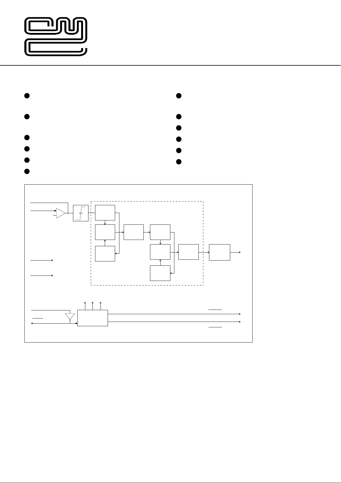
Fig.1 Functional Block Diagram
Brief Description
The FX002 is a single-chip device to extract single
periodic signals from very high random-noise
environments.
Using patented autocorrelation techniques the
FX002 will enhance the input signal's signal-to-noise
ratio by as much as 8.5dB and provide a digital output
signal centred at four times (x4) the input frequency.
The amplitude of non-periodic components of the
signal is substantially reduced. The patented
autocorrelator compares the incoming signal to itself;
the more elements of the waveform that are seen as
periodic, the higher the energy at the microcircuit
output.
The FX002 cascades two autocorrelators, each one
improving the signal-to-noise ratio.
OUTPUT
[4 x SIGNAL IN]
INTERPOLATE
OUTPUT
LOGIC
FX002
CLOCK
OUTPUT
6
CLOCK
OUTPUT
24
With a random noise input the output will swing
rail-to-rail at random (peak-limited). The input/output
signal delay is fixed by the choice of clock frequency
and the length of the internal register. The FX002 will
operate at supply voltages of between 2.5 volts and
5.5 volts and with Xtal/clock frequencies from 20kHz to
2.5MHz. Using various Xtal/clock inputs the device can
be set to accept input signal frequencies, in bands,
from 17.0Hz to 13.0kHz.
Two uncommited clock outputs are available to
supply 'divided-down' Xtal/clock frequencies for use in
external and peripheral functions.
This low-power signal processing device is
available in 16-pin cerdip dual-in-line (DIL) and plastic
small outline (S.O.I.C.) surface mount packages.
1
Page 2
Pin Number Function
FX002DW
1
3
4
5
6
8
FX002J
1
3
4
5
6
7
Signal In: The inverting input to the analogue amplifier/comparator. Used with the Signal Bias
pin; external coupling components are required (see Figure 2).
Signal Bias: The output of the analogue amplifier/comparator. Do not load this pin with
peripheral circuitry; there is no drive capacity for off-chip signalling. The feedback resistor
should be not less than 200kΩ. See Figure 2.
VDD: Positive supply rail. A single, stable power supply is required. Note that this device has
two VDD pins; this input is positioned to prevent cross-talk, either or both may be connected to
the host circuit's supply line. Do not attempt to draw current from either VDD pin.
Clock/24: A squarewave output clock signal at the rate of
Xtal/clock
/24; provided for peripheral
and test purposes.
Xtal: The output of the on-chip clock oscillator inverter.
Xtal/Clock: The input to the on-chip clock oscillator inverter; this may be a Xtal, resonator or
clock pulse input. The selection of this frequency will affect the operational input signal
bandwidth (and output frequency) of this device; refer to Table 2. Note that the choice of V
DD
will determine the maximum Xtal/clock frequency and hence the maximum useable signal
input frequency. Operation of any CML microcircuit without an active Xtal or clock input may
cause device damage. A clock pulse input is fed directly into this pin; Xtal/clock components
are not required.
Table 1 provides a guide to maximum usable Xtal/clock frequencies at pre-determined V
DD
values.
V
(V) Max. Xtal/Clock
DD
Freq. (MHz)
2.5 0.625
Table 1
3.0 1.0
5.0 2.5
9
11
13
16
2, 7, 10,
12, 14, 15
9
11
13
16
2, 8,
10, 12,
14, 15
VSS: Negative supply rail (GND).
Clock/6: A squarewave output clock signal at the rate of
Xtal/clock
/6; provided for peripheral
and test purposes.
Output: (f
OUT
= 4 x f
). The auto-correlated output signal at four times (x 4) the input
SIGNAL IN
signal (see Figure 4).
There is a time delay between input and output signals (see Specifications).
VDD: Positive supply rail. A single, stable power supply is required.
Note that this device has two VDD pins; either or both may be connected to the host circuit's
supply line. Do not attempt to draw current from either VDD pin.
The choice of VDD will determine the maximum Xtal/clock frequency and hence the maximum
useable signal input frequency (see Figure 3).
No internal connection. Leave open-circuit.
2
Page 3

Application Information
External Components
OUTPUT
R
2
SIGNAL IN
SIGNAL BIAS
R
XTAL
6
XTAL/CLOCK
7
SIGNAL
INPUT
XTAL/CLOCK
C
3
C
2
V
SS
XTAL/CLOCK
C
1
V
DD
4
XTAL
X
1
C
4
Fig.2 Recommended External Components
V
DD
C
5
1
x
2
3
1
4
5
FX002J
6
7
x
8
V
16
15
14
13
12
11
10
9
SS
V
DD
x
x
OUTPUT
x
CLOCK
x
V
SS
(f = 4 x SIGNAL IN)
OUTPUT
6
V
SS
Xtal/Clock Input Freq. (Hz)
Freq. (kHz) Min Max BW (Hz)
20 17 105 88
100 88 526 443
200 166 1052 886
300 250 1579 1329
400 333 2105 1772
500 416 2632 2216
560 467 2947 2480
600 500 3158 2658
700 583 3684 3101
800 667 4210 3543
900 750 4737 3987
1000 833 5263 4430
2000 1667 10526 8859
2500 2083 13157 11074
Table 2 Input Signal Ranges vs Xtal/Clock Frequency
14000
12000
10000
Minimum Input Frequency =
Xtal/Clock Frequency (Hz)
1200
Component Value for VDD = 5.0V
R
1
R
2
C
1
C
2
C
3
C
4
C
5
X
1
X1 range 20kHz to 2.5MHz
Table 3 Recommended External Components
Xtal/Clock Components
C4 is suggested for frequency setting when using a
resonator; when a Xtal is used C4 is omitted. Values
of capacitors C2 and C3 should be reduced for higher
Xtal frequencies and/or lower supply voltages (VDD).
Maximum Input Frequency =
Xtal/Clock Frequency (Hz)
190
2.2MΩ
1.0MΩ
0.01µF
47.0pF -see below
47.0pF -see below
5 - 65pF -see below
1.0µF
560kHz resonator
Maximum Input Frequency (Hz)
DD
=5.0V
For V
Maximum Clock Limit
=3.0V
at V
DD
Input Signal Frequency (Hz)
8000
6000
4000
2000
Maximum Clock Limit
at V
=2.5V
DD
0
0 500 1000 1500 2000 2500
Fig.3 Examples of Input Signal Ranges vs Xtal/Clock Frequency
3
Input Signal Bandwidth (Hz)
Minimum Input Frequency (Hz)
Xtal/Clock Frequency (kHz)
Page 4

Application Information ......
Level
Frequency
SIGNAL IN
f
SIGNAL IN
SIGNAL OUT
f
OUT
=4xf
SIGNAL IN
Fig.4 Example FX002 Input/Output Relationships
The diagrams in Figure 4 are example spectrums of the input and output signal conditions of the FX002.
Note that the frequency of the output signal is four times (x4) that of the input signal.
The graph shown in Figure 5 illustrates the signal-to-noise enhancement that can be obtained, under varying
input conditions, from the FX002.
Effective Output Signal-to-Noise Ratio (dB)
9
8
7
6
5
Input Signal = 2.7kHz 20mV r ms
Xtal/Clock Frequency 500kHz
V
=5.0V
DD
4
3
2
1
-6 -5 -4 -3 -2 -1 0 1 2 3 4 5 6 7 8
Input Signal-to-Noise Ratio (dB)
Fig.5 Enhancement of Signal-To-Noise Ratio
4
Page 5

Specification
Absolute Maximum Ratings
Exceeding the maximum rating can result in device damage. Operation of the device outside the operating
limits is not implied.
Supply voltage -0.3 to 7.0V
Input voltage at any pin (ref V
Sink/source current (supply pins) +/- 30mA
(other pins) +/- 20mA
Total device dissipation @ T
Derating 10mW/°C
Operating temperature range: FX002DW -40°C to +85°C
Storage temperature range: FX002DW -40°C to +85°C
Operating Limits
Correct operation of the device outside these limits is not implied.
Supply Voltage (VDD) Note 1 2.5 5.5 V
Operating Temperature -40.0 +85.0 °C
Xtal/Clock Frequency (VDD = 2.5V) 20.0 625 kHz
= 0V) -0.3 to (V
SS
25°C 800mW Max.
AMB
FX002J -40°C to +85°C
FX002J -55°C to +125°C
Remarks Min. Max. Unit
(VDD = 5.0V) 0.02 2.5 MHz
+ 0.3V)
DD
Operating Characteristics
All device characteristics are measured under the following conditions unless otherwise specified:
V
= 5.0V, T
DD
= 25°C. Xtal/Clock Frequency = 560kHz. Input Test Signal = 1.0kHz at 200mVrms.
AMB
Characteristics See Note Min. Typ. Max. Unit
Static Values
Supply Current (IDD) - 1.0 2.5 mA
2 - 4.0 - mA
Output Logic ‘1’ 80% - - V
Output Logic ‘0’ - - 20% V
Digital Output Impedance - 4.0 10.0 kΩ
Dynamic Values
Signal Input Levels 3 10.0 20.0 1000 mVrms
Analogue (Input) Amplifier Gain 4 20.0 - - dB
5 9.0 - - dB
6 10.0 - - dB
Recommended Input Signal Mark-to-Space Ratio 35.0 - - %
Freq. In/Freq. Out Ratio 4.0 4.0
Maximum Xtal/Clock Frequency 1 2.5 - - MHz
Minimum Xtal/Clock Frequency - - 20.0 kHz
Frequency Input Range (Xtal/Clock = 560kHz) 500 - 3000 Hz
(Table 2) 7 1/1200 1/190 Xtal/Clock
Input to Output Delay 8 - 1.4 - ms
Output Resolution - 1/6 - Xtal/Clock
DD
DD
Notes
1. Maximum Xtal/clock frquency allowed varies with applied supply voltage (VDD).
2. IDD requirement for Xtal/clock frequency of 2.24MHz.
3. Signal input level required to provide a constant autocorrelated output.
4. Measured with a 6.0kHz sinewave at the signal input.
5. Measured with VDD = 2.5 volts.
6. Measured with a 12kHz input signal.
7. Recommended input signal frequency range to correlation circuits.
8. Input (Signal In) to output (Output) time with a 2.24MHz Xtal/clock input.
5
Page 6

Package Outlines
The FX002 is available in the package styles outlined
below. Mechanical package diagrams and specifications
are detailed in Section 10 of this document.
Pin 1 identification marking is shown on the relevant
diagram and pins on all package styles number
anti-clockwise when viewed from the top.
Handling Precautions
The FX002 is a CMOS LSI circuit which includes input
protection. However precautions should be taken to
prevent static discharges which may cause damage.
FX002J 16-pin cerdip DIL (J2)FX002DW 16-pin plastic S.O.I.C. (D4)
NOT TO SCALE
Max. Body Length 10.49mm
Max. Body Width 7.59mm
NOT TO SCALE
Max. Body Length 19.48mm
Max. Body Width 7.39mm
Ordering Information
FX002DW 16-pin plastic S.O.I.C. (D4)
FX002J 16-pin cerdip DIL (J2)
CML does not assume any responsibility for the use of any circuitry described. No circuit patent licences are implied
and CML reserves the right at any time without notice to change the said circuitry.
6
 Loading...