

Page 1

Features/Applications
CML Semiconductor Products
PRODUCT INFORMATION
Duplex Frequency Inverter
FX118
for Cordless Telephones
Publication D/118/3 July 1994
Frequency Inversion Scrambling
Full-Duplex Operation
High Baseband and Carrier
Rejection
Audio Lowpass and Bandpass
Filtering On-Chip
Xtal Oscillator Stabilty
C1 AMP OUT
C1 IN
INPUT AMP
XTAL/CLOCK
XTAL
INPUT AMP
C2 IN
V
BIAS
V
BIAS
LPF(1) OUT B MOD(1) IN
LPF(1)
+0.5dB
+0.5dB
LPF(2) BAL MOD (2)
CHANNEL 1 (C1)
CHANNEL 2 (C2)
LPF(2) OUT B MOD(2) INC2 AMP OUT
CLOCKS
and
LOGIC
FILTER CLOCKS
111kHz
BAL MOD (1) BPF(1)
-4.0dB
CARRIER
3.3kHz
-4.0dB
Low Power Requirement
(3.0 Volt Minimum)
Cordless Telephones
Base and Handheld Applications
Input Gain Adjustment
Plastic DIL and S.O.I.C. Package
Styles
C1 OUT
+4.0dB
V
DD
V
BIAS
FX118
+4.0dB
BPF(2)
V
SS
C2 OUT
Fig.1 FX118 Duplex Frequency Inverter
Brief Description
The FX118 is a low-power, full-duplex frequency
inverter available to provide voice privacy for cordless
telephone systems by mixing the incoming audio with an
internally produced carrier frequency (3.3kHz).
This chip contains two completely separate audio
channels (C1 and C2) each comprising a “componentadjustable” input amplifier, a 10th-order lowpass filter, a
balanced modulator and a 14th-order bandpass filter
output.
The on-chip modulation process has the properties of
high baseband and carrier frequency rejection which
when combined with high-order output filtering,
produces a high-quality recovered voiceband audio.
The frequency stability of the FX118 is achieved by an
on-chip oscillator employing an external 4.433619MHz
Xtal or clock input to produce the common carrier
frequency and the sampling clocks for the switched
capacitor low and bandpass filters.
This microcircuit has a low power requirement of 3.0
volts (min.) and is encapsulated in either 16-pin DIL or
small outline SMD (S.O.I.C.) plastic packages both of
which are of a physical size suitable for either base or
handset type telephone instruments as well as batteryportable and mobile communications systems.
1
Page 2

Pin Number Function
FX118DW
FX118P
1
2
3
Xtal: Output of clock oscillator inverter.
No Internal Connection: It is recommended that, to improve noise conditions, this pin is connected to V
LPF(1) Out: The output of the Channel 1 Lowpass Filter. It is to be coupled to “B Mod(1) In” via a 1.0µF
.
SS
capacitor – see Figure 2.
4
B Mod(1) In: The input to Channel 1 balanced modulator. Internally biased at V
“LPF(1)” via a 1.0µF capacitor – see Figure 2.
V
5
6
7
: Negative supply (GND).
SS
C1 Out: The analogue output of Channel 1.
C1 Amp Output: Channel 1 amplifier with external components (see Figure 2) can be used to provide gain in
/2 it is to be coupled to
DD
the signal path.
10
11
12
13
14
8
9
C1 In: The negative input of Channel 1 Amplifier. Recommended external components are shown in Figure 2.
C2 In: The negative input of Channel 2 Amplifier. Recommended external components are shown in Figure 2.
C2 Amp Output: Channel 2 amplifier with external components (see Figure 2) can be used to provide gain in
the signal path.
C2 Out: The analogue output of Channel 2.
V
: The internal analogue bias line at VDD/2. It should be decoupled to VSS via a 1.0µF or greater capacitor.
BIAS
See Figure 2.
B Mod(2) In: The input to Channel 2 balanced modulator. Internally biased at V
“LPF(2)” via a 1.0µF capacitor – see Figure 2.
/2 it is to be coupled to
DD
LPF(2) Out: The output of the Channel 2 Lowpass Filter. It is to be coupled to “B Mod(2) In” via a 1.0µF
capacitor – see Figure 2.
15
16
VDD: The positive supply rail. A single positive supply voltage (3.0v – 5.0v) is required. Levels and voltages
within the Duplex Frequency Inverter are dependent upon this supply.
Xtal/Clock: 4.433619 MHz Xtal or externally derived clock is injected at this pin. See Figure 2. Operation of
the FX118 without a Xtal or clock input may cause device damage.
2
Page 3
Application Information
C
3
V
DD
C
2
X
C
1
1
R
1
XTAL
LPF(1) OUT
C
4
B MOD(1) IN
V
C1 OUT
CHANNEL 1 OUTPUT
CHANNEL 1 INPUT
R
C
2
5 R
R
3
C1 AMP OUT
C1 IN
1
2
3
4
SS
FX118
5
6
7
16
15
14
13
12
11
10
89
V
SS
XTAL/CLOCK
V
DD
LPF(2) OUT
B MOD(2) IN
V
BIAS
C2 OUT
C2 AMP OUT
C2 IN
C
V
SS
R
5
Component Value
R
1
R2 R3 C
R4 R5 C
C
1
5
6
= 1.0MΩ
See Note
See Note
47pF
C
2
C
3
C
4
T
olerances C = ±20% R = ±10%
= 33pF
0.47µF
1.0µF
C
7
C
8
X
1
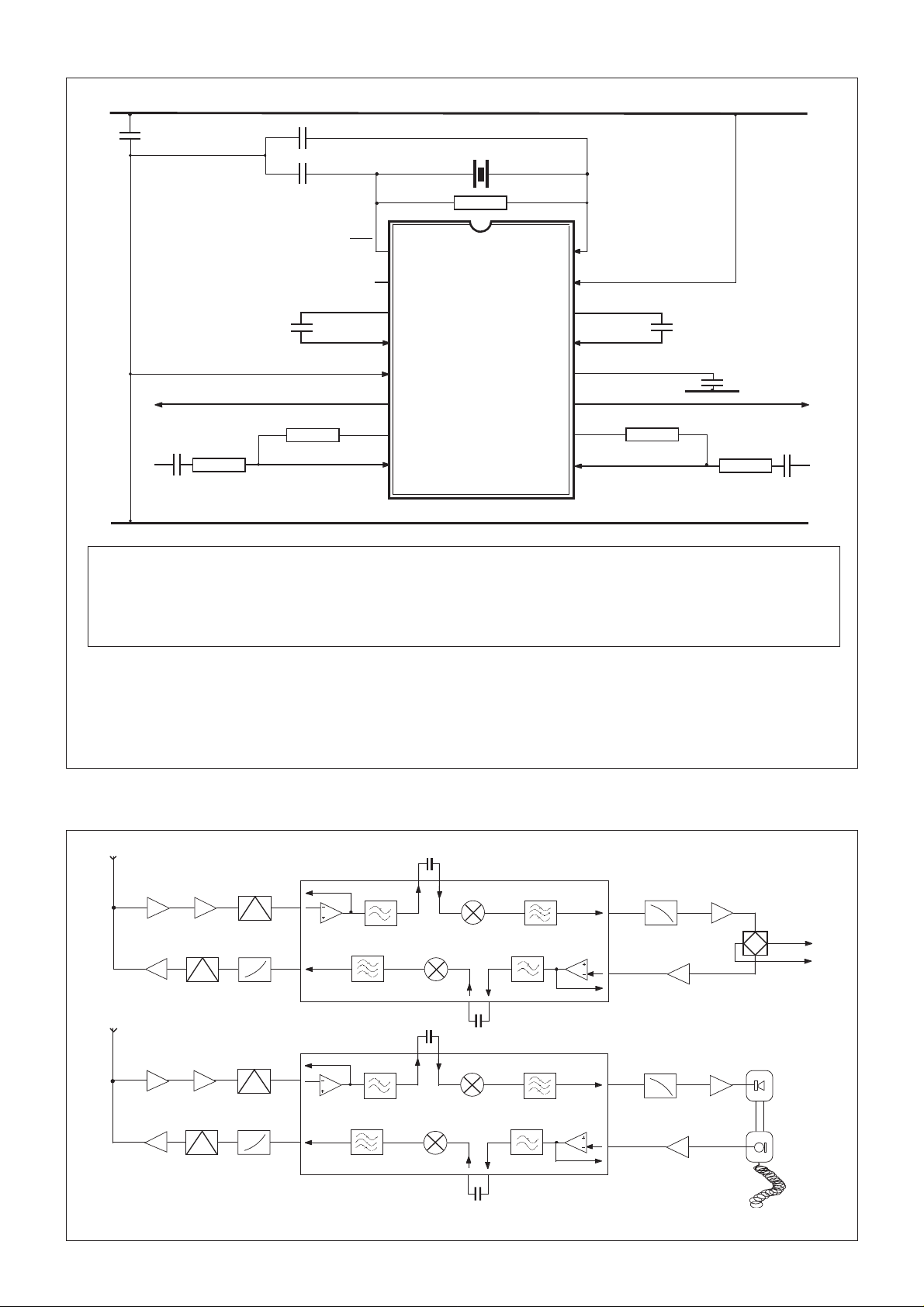
NOTES 1. Configurations R2, R3, C5 and R4, R5, C6 should be chosen with respect to the specific application.
2. Operation of any CML microcircuit without a Xtal or clock input may cause device damage. To minimise damage
in the event of a Xtal/drive failure, it is recommended that the power rail (VDD) is fitted with a current limiting
device (resistor or fast-reaction fuse).
8
C
7
CHANNEL 2 OUTPUT
CHANNEL 2 INPUT
= 1.0µF
C
4
6
1.0µF
4.433619MHz
Fig.2 Recommended External Components
Rx Channel
RF
IF
AMP
MODULATION
FM
Tx Channel
Rx Channel
IF
AMP
MODULATION
FM
Tx Channel
DETECTION
FM
PRE-
EMPHASIS
DETECTION
FM
PRE-
EMPHASIS
AMP
AMP
AMP
AMP
RF
RF
RF
CHANNEL 1 (C1)
CHANNEL 1 (C1)
CHANNEL 2 (C2)
CHANNEL 2 (C2)
BASE UNIT
FX118
FX118
HANDHELD UNIT
DE-EMPHASIS
DE-EMPHASIS
AF AMP
AF AMP
AF AMP
HYBRID
TRANSFORMER
AF AMP
TELEPHONE
LINE
Fig.3 Example of the FX118 Employed in a Cordless Telephone Application
3
Page 4
Application Information ......
Gain
+5
dB
0
-3
-10
-20
-30
-40
0.1 0.2 0.3 0.5 2.01.0 7.0
Audio Input Level = 275mVrms
V = 3.75V
DD
3.0
Frequency kHz
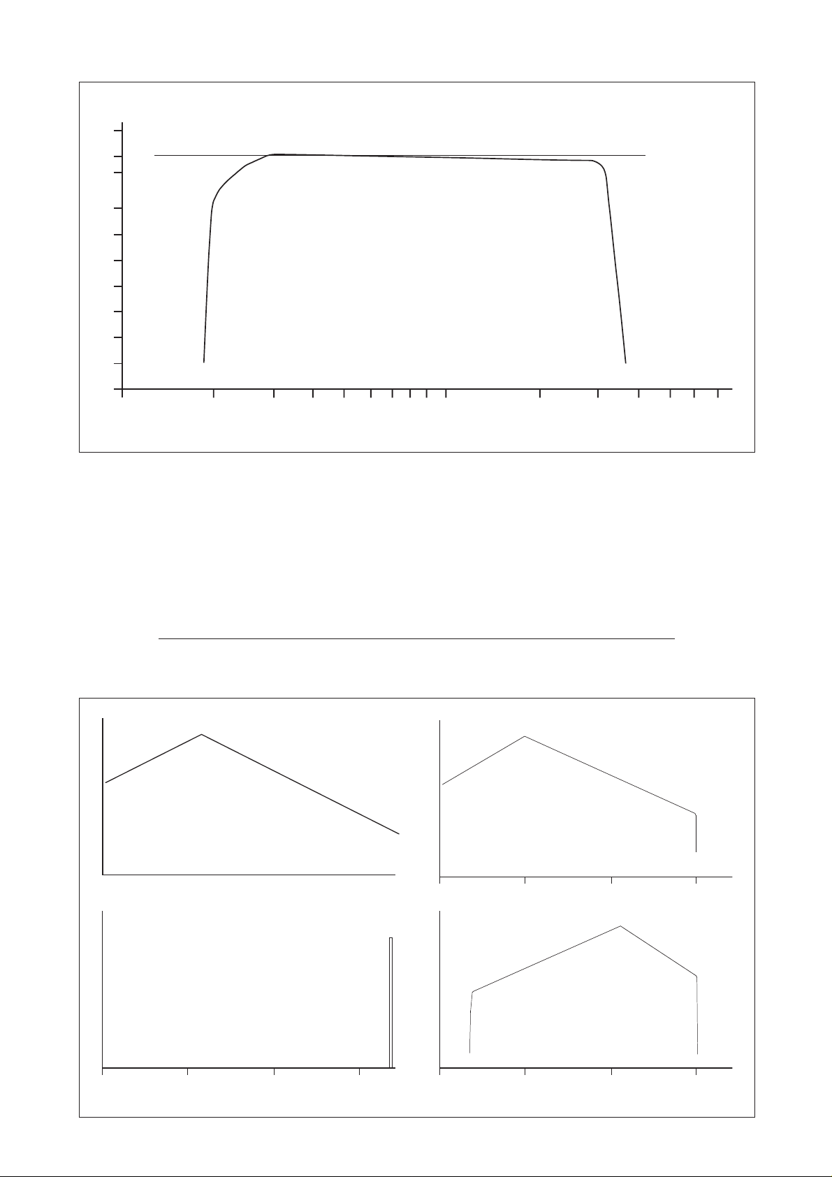
Fig.4 Typical Audio Frequency Response of a Single Scrambled or De-scrambled Channel
System Gains
When calculating the external components for the operation of the FX118 the following points should be considered:
(a) The Input Lowpass Filter has a (typical) gain of 0.5dB.
(b) The Balanced Modulator has a (typical) attenuation of 4.0dB.
(c) The Output Bandpass Filter has a (typical) gain of 4.5dB.
How the Inverter Works
Carrier Frequency
(1)
Input Voiceband Frequencies
(3)
minus
Input Voice Frequency
Speech Band
Carrier Frequency (3300Hz)
Generated On-Chip for Input to
Balanced Modulator
equals
Scrambled Voice Frequency
(2)
B
A
Lowpass Filtered Voiceband
Balanced Modulator
0
(4)
D
Bandpass Filtered Voiceband
after Mixing with the Carrier Frequency
in the Balanced Modulator
C
D
for Input to
1000Hz 2000Hz 3000Hz
B
C
A
Presented at the Ouput
0
1000 2000 3000
3300
0
Fig.5 A Pictorial Explanation of the FX118 “Scramble Operation”
4
1000 2000 3000
Page 5

Specification
Absolute Maximum Ratings
Exceeding the maximum rating can result in device damage. Operation of the device outside the operating limits is not
implied.
Supply voltage -0.3 to 7.0V
Input voltage at any pin (ref V
Sink/source current (supply pins) +/- 30mA
(other pins) +/- 20mA
Total device dissipation @ T
Derating 10mW/°C
Operating temperature range: FX118DW/P -40°C to +85°C
Storage temperature range: FX118DW/P -40°C to +85°C
Operating Limits
All device characteristics are measured under the following conditions unless otherwise specified:
V
= 3.75V. T
DD
= 25°C. Xtal/Clock f0 = 4.433619MHz. Audio level 0dB ref: = 388mV rms @ 1.0kHz.
AMB
Characteristics See Note Min. Typ. Max. Unit
Static Values
Supply Voltage 3.0 3.75 5.5 V
Supply Current – 4.0 6.0 mA
Input Impedance (Amplifiers) 1.0 10.0 – MΩ
Output Impedance (LP Filters) – 2.0 – kΩ
Output Impedance (C1, C2 ) – 200 – Ω
Output Impedance (C1, C2 Amps) – 10.0 – kΩ
On-Chip Xtal Oscillator
R
IN
R
OUT
Inverter Gain – 10.0 – V/V
Gain/Bandwidth Product – 10.0 – MHz
Dynamic Values
Analogue Signal Input Levels -16.0 – 4.0 dB
SINAD 6 – 30.0 – dB
Unwanted Modulation Products 1, 2 – -40.0 – dB
Carrier Breakthrough 1, 2 – -55.0 – dB
Baseband Breakthrough 1, 2 – -40.0 – dB
Carrier Frequency – 3299 – Hz
Analogue Output Noise 3 – -42.0 – dB
Analogue Output Noise 5 – -46.0 – dBp
Filters
Input Lowpass Filter 1
Cut-Off Frequency (-3dB) – 3100 – Hz
Passband Ripple (300Hz - 3kHz) – ±1.0 – dB
Attenuation at 3.3kHz – 30.0 – dB
Attenuation at 3.6kHz – 45.0 – dB
Passband Gain – 0.5 – dB
Output Bandpass Filter 1, 4
Passband Frequencies 300 – 3000 Hz
Passband Ripple – ±1.0 – dB
Low Freq. Roll-Off <200Hz 12.0 – – dB/oct.
High Freq. – Attenuation at 3.4kHz – 48.0 – dB
Passband Gain 3.5 4.5 5.5 dB
Overall Modulated and De-Modulated Channel Response
Passband Frequencies (Tx and Rx Channel) 300 – 3000 Hz
Passband Ripple -3.0 – 2.0 dB
Low Freq. Roll-Off <250Hz 18.0 – – dB/oct.
High Freq. – Attenuation at 3.4kHz – 48.0 – dB
Passband Gain 4 – 0.5 – dB
Distortion 1 – 3.0 – %
= 0V) -0.3 to (V
SS
25°C 800mW Max.
AMB
10.0 – – MΩ
– 10.0 – kΩ
+ 0.3V)
DD
Notes:
1. Measured with an audio input level of -3.0dB.
2. With respect to a single modulated (scrambling) channel.
3. Measured with a short circuit input, at any analogue output, in a 30.0kHz bandwidth.
4. With Input Amplifier gain at 0dB.
5. Measured psophometrically weighted, at any analogue output.
6. Measured in a 30kHz bandwidth.
5
Page 6
Package Outlines
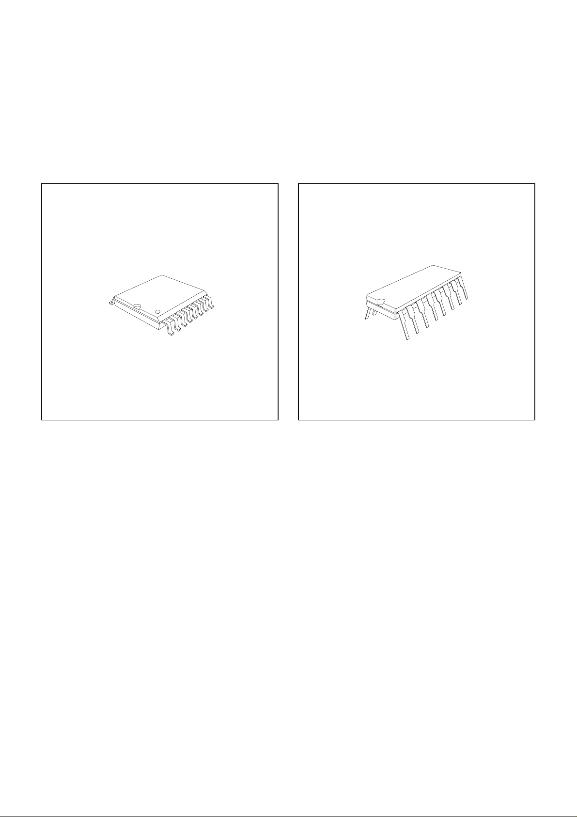
The FX118 is available in the package styles outlined
below. Mechanical package diagrams and specifications
are detailed in Section 10 of this document.
Pin 1 identification marking is shown on the relevant
diagram and pins on all package styles number
anti-clockwise when viewed from the top.
Handling Precautions
The FX118 is a CMOS LSI circuit which includes input
protection. However precautions should be taken to
prevent static discharges which may cause damage.
FX118DW 16-pin S.O.I.C. (D4)
NOT TO SCALE
Max. Body Length 10.49mm
Max. Body Width 7.59mm
FX118P 16-pin plastic DIL (P3)
NOT TO SCALE
Max. Body Length 20.57mm
Max. Body Width 6.60mm
Ordering Information
FX118DW 16-pin S.O.I.C. (D4)
FX118P 16-pin plastic DIL (P3)
CML does not assume any responsibility for the use of any circuitry described. No circuit patent licences are implied
and CML reserves the right at any time without notice to change the said circuitry.
6
 Loading...