

Page 1

E
4/9/97 2:23 PM PIIX4aDS
INTEL CONFIDENTIAL
(until publication date)
© INTEL CORPORATION 1997 April 1997 Order Number: 290562-001
Supported Kits for both Pentium® and
Pentium
®
II Microprocessors
82430TX ISA Kit
82440LX ISA/DP Kit
Multifunction PCI to ISA Bridge
Supports PCI at 30 MHz and 33 MHz
Supports PCI Rev 2.1 Specification
Supports Full ISA or Extended I/O
(EIO) Bus
Supports Full Positive Decode or
Subtractive Decode of PCI
Supports ISA and EIO at 1/4 of PCI
Frequency
Supports both Mobile and Desktop
Deep Green Environments
3.3V Operation with 5V Tolerant
Buffers
Ultra-low Power for Mobile
Environments Support
Power-On Suspend, Suspend to
RAM, Suspend to Disk, and SoftOFF System States
All Registers Readable and
Restorable for Proper Resume
from 0.V Suspend
Power Management Logic
Global and Local Device
Management
Suspend and Resume Logic
Supports Thermal Alarm
Support for External
Microcontroller
Full Support for Advanced
Configuration and Power Interface
(ACPI) Revision 1.0 Specification
and OS Directed Power
Management
Integrated IDE Controller
Independent Timing of up to
4 Drives
PIO Mode 4 and Bus Master IDE
Transfers up to 14 Mbytes/sec
Supports “Ultra DMA/33”
Synchronous DMA Mode Transfers
up to 33 Mbytes/sec
Integrated 16 x 32-bit Buffer for IDE
PCI Burst Transfers
Supports Glue-less “Swap-Bay”
Option with Full Electrical Isolation
Enhanced DMA Controller
Two 82C37 DMA Controllers
Supports PCI DMA with 3 PC/PCI
Channels and Distributed DMA
Protocols (Simultaneously)
Fast Type-F DMA for Reduced PCI
Bus Usage
Interrupt Controller Based on Two
82C59
15 Interrupt Support
Independently Programmable for
Edge/Level Sensitivity
Supports Optional I/O APIC
Serial Interrupt Input
Timers Based on 82C54
System Timer, Refresh Request,
Speaker Tone Output
USB
Two USB 1.0 Ports for Serial
Transfers at 12 or 1.5 Mbit/sec
Supports Legacy Keyboard and
Mouse Software with USB-based
Keyboard and Mouse
Supports UHCI Design Guide
SMBus
Host Interface Allows CPU to
Communicate Via SMBus
Slave Interface Allows External
SMBus Master to Control Resume
Events
Real-Time Clock
256-byte Battery-Back CMOS SRAM
Includes Date Alarm
Two 8-byte Lockout Ranges
Microsoft Win95* Compliant
324 mBGA Package
82371AB PCI-TO-ISA / IDE
XCELERATOR (PIIX4)
Page 2

82371AB (PIIX4) E
2
4/9/97 2:23 PM PIIX4aDS
INTEL CONFIDENTIAL
(until publication date)
PRELIMINARY
The 82371AB PCI ISA IDE Xcelerator (PIIX4) is a multi-function PCI device implementing a PCI-to-ISA bridge
function, a PCI IDE function, a Universal Serial Bus host/hub function, and an Enhanced Power Management
function. As a PCI-to-ISA bridge, PIIX4 integrates many common I/O functions found in ISA-based PC
systems—two 82C37 DMA Controllers, two 82C59 Interrupt Controllers, an 82C54 Timer/Counter, and a Real
Time Clock. In addition to compatible transfers, each DMA channel supports Type F transfers. PIIX4 also
contains full support for both PC/PCI and Distributed DMA protocols implementing PCI-based DMA. The
Interrupt Controller has Edge or Level sensitive programmable inputs and fully supports the use of an external
I/O Advanced Programmable Interrupt Controller (APIC) and Serial Interrupts. Chip select decoding is provided
for BIOS, Real Time Clock, Keyboard Controller, second external microcontroller, as well as two Programmable
Chip Selects. PIIX4 provides full Plug and Play compatibility. PIIX4 can be configured as a Subtractive Decode
bridge or as a Positive Decode bridge. This allows the use of a subtractive decode PCI-to-PCI bridge such as
the Intel 380FB PCIset which implements a PCI/ISA docking station environment.
PIIX4 supports two IDE connectors for up to four IDE devices providing an interface for IDE hard disks and CD
ROMs. Up to four IDE devices can be supported in Bus Master mode. PIIX4 contains support for “Ultra DMA/33”
synchronous DMA compatible devices.
PIIX4 contains a Universal Serial Bus (USB) Host Controller that is Universal Host Controller Interface (UHCI)
compatible. The Host Controller’s root hub has two programmable USB ports.
PIIX4 supports Enhanced Power Management, including full Clock Control, Device Management for up to
14 devices, and Suspend and Resume logic with Power On Suspend, Suspend to RAM or Suspend to Disk. It
fully supports Operating System Directed Power Management via the Advanced Configuration and Power
Interface (ACPI) specification. PIIX4 integrates both a System Management Bus (SMBus) Host and Slave
interface for serial communication with other devices.
Information in this document is provided in conjunction with Intel products. No license, express or implied, by estoppel or
otherwise, to any intellectual property rights is granted by this document or by the sale of Intel products. Except as provided in
Intel’s Terms and Conditions of Sale for such products, Intel assumes no liability whatsoever, and Intel disclaims any express
or implied warranty, relating to sale and/or use of Intel products including liability or warranties relating to fitness for a particular
purpose, merchantability, or infringement of any patent, copyright or other intellectual property right. Intel products are not
intended for use in medical, life saving, or life sustaining applications.
Intel retains the right to make changes to specifications and product descriptions at any time, without notice.
The 82371AB PIIX4 may contain design defects or errors known as errata. Current characterized errata are available
on request.
Intel disclaims all liability, including liability for infringement of any proprietary rights, relating to use of information in this
specification. Intel does not warrant or represent that such use will not infringe such rights.
I2C is a two-wire communication bus/protocol developed by Philips. SMBus is a subset of the I2C bus/protocol and was
developed by Intel. Implementation of the I2C bus/protocol or the SMBus bus/protocol may require licenses from various
entities, including Philips Electronics N.V. and North American Philips Corporation.
Third-party brands and names are the property of their respective owners.
Page 3
E 82371AB (PIIX4)
3
4/9/97 2:23 PM PIIX4aDS
INTEL CONFIDENTIAL
(until publication date)
PRELIMINARY
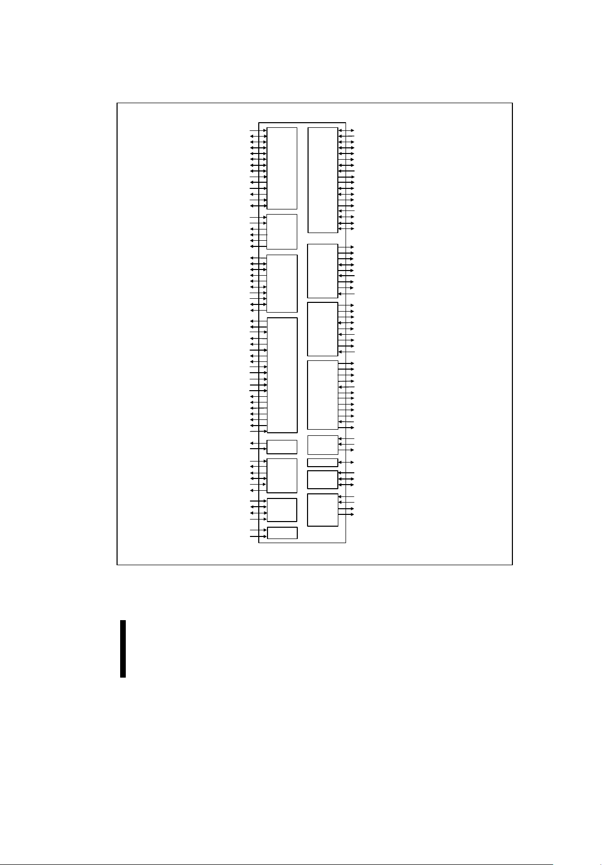
PCICL
K
AD[31:0]
C/BE[3:0]#
FRAME#
TRDY#
IRDY#
STOP#
DEVSEL#
SERR#
PAR
IDSEL
PHOLD#
PHLKA#
CLKR
UN#
RCIN#
PWROK
CPURST
RSTDRV
INIT
PCIRST#
IRQ0//GPO14
IRQ8#/GPI6
IRQ12/M
INTR
NMI
IRQ[15,14,11:9,7:3,1]
SERIRQ/GPI7
PRIQ[A:C]
PIRQD
IRQ9OUT#/GPO29
SMI#
STPCLK#
EXTSMI#
SLP#
SUSCLK
BATLOW#/GPI9
THRM#/GPI8
LID//GPI10
RI#/GPI12
RSMRST#
PWRBTN#
SUSA#
SUSB#/GPO15
SUSC#/GPO16
ZZ/GPO19
PCIREQ[D:A]#
SPKR
OSC
DREQ[7:5,3:0]
DACK[7:5,3:0]#
TC
REFRESH#
REQ[A:C]#/GPI[2:4]
GNT[A:C]#/GPO[9:11]
CLK48
USBPO±
USBP1±
OC[1:0]#
CONFIG[2:1]
TEST#
PCI Bus
Interface
ISA Bus
Interface
System
Reset
Interrupt
Primary
IDE
Interface
Secondary
IDE
Interface
System
Power
Mgmt.
X-Bus
Support
Logic
Timers/
Counters
DMA
I/O APIC
Support
Logic
Universal
Serial
Bus
RTC
SMBUS
General
Purpose
Inputs
and
Outputs
Test
SD[15:0]
IOCS16#
MEMCS16#
MEMR#
MEMW#
AEN
IOCHRDY
IOCHK#/GPI0
SYSCLK
BALE
IOR#
IOW#
SMEMR#
SMEMW#
ZEROWS#
SA[19:0]
LA[23:17]/GPO[7:1]
SBHE#
PDCS1#
PDCS3#
PDA[2:0]
PDD[15:0]
PDDACK#
PDDREQ
PDIOIR#
PDIOW#
PIORDY
SDCS1#
SDCS3#
SDA[2:0]
SDD[15:0]
SDDACK#
SDDREQ
SDIOR#
SDIOW#
SIORDY
PCS[1:0]#
XDIR#/GPO22
XOE#/GPO23
RTCALE/GPO25
FERR#
IGNNE#
BIOSCS#
RTCCS#/GPO24
KBCCS#/GPO26
A20M#
A20GATE
MCCS#
APICCS#/GPO13
APICACK#/GPO12
APCIREQ#/GPI5
RTCX[2:1]
SMBALERT#
SMBCLK
SMBDATA
GPI[21:13,1]
GPI[12:2,0] (Multiplexed)
GPO[30,28:27,8,0]
GPO[29,26:9,7:1] (Multiplexed)
Pix4_blk
Simplified Block Diagram
Page 4

82371AB (PIIX4) E
4
4/9/97 2:23 PM PIIX4aDS
INTEL CONFIDENTIAL
(until publication date)
PRELIMINARY
CONTENTS
PAGE
1.0. ARCHITECTURAL OVERVIEW....................................................................................................................12
2.0. SIGNAL DESCRIPTION................................................................................................................................15
2.1. PIIX4 Signals ..............................................................................................................................................16
2.1.1. PCI Bus Interface.................................................................................................................................16
2.1.2. ISA Bus Interface.................................................................................................................................18
2.1.3. X-Bus Interface....................................................................................................................................21
2.1.4. DMA Signals........................................................................................................................................23
2.1.5. Interrupt Controller/APIC Signals.........................................................................................................24
2.1.6. CPU Interface Signals .........................................................................................................................26
2.1.7. Clocking Signals..................................................................................................................................28
2.1.8. IDE Signals..........................................................................................................................................28
2.1.9. Universal Serial Bus Signals ...............................................................................................................33
2.1.10. Power Management Signals..............................................................................................................33
2.1.11. General Purpose Input and Output Signals.......................................................................................35
2.1.12. Other System and Test Signals.........................................................................................................39
2.1.13. Power and Ground Pins.....................................................................................................................39
2.2. Power Planes..............................................................................................................................................40
2.3. Power Sequencing Requirements..............................................................................................................41
3.0. REGISTER ADDRESS SPACE.....................................................................................................................42
3.1. PCI/ISA Bridge Configuration.....................................................................................................................42
3.1.1. PCI Configuration Registers (Function 0)............................................................................................43
3.1.2. IO Space Registers .............................................................................................................................44
3.2. IDE Configuration........................................................................................................................................47
3.2.1. PCI Configuration Registers (Function 1)............................................................................................47
3.2.2. IO Space Registers .............................................................................................................................48
3.3. Universal Serial Bus (USB) Configuration..................................................................................................48
3.3.1. PCI Configuration Registers (Function 2)............................................................................................48
3.3.2. IO Space Registers .............................................................................................................................49
3.4. Power Management Configuration .............................................................................................................50
3.4.1. IO Space Registers .............................................................................................................................51
4.0. PCI TO ISA/EIO BRIDGE REGISTER DESCRIPTIONS..............................................................................53
4.1. PCI to ISA/EIO Bridge PCI Configuration Space Registers (PCI Function 0)............................................53
4.1.1. VID—Vendor Identification Register (Function 0)................................................................................53
4.1.2. DID—Device Identification Register (Function 0)................................................................................53
4.1.3. PCICMD—PCI Command Register (Function 0) ................................................................................54
4.1.4. PCISTS—PCI Device Status Register (Function 0)............................................................................55
4.1.5. RID—Revision Identification Register (Function 0).............................................................................55
Page 5

E 82371AB (PIIX4)
5
4/9/97 2:23 PM PIIX4aDS
INTEL CONFIDENTIAL
(until publication date)
PRELIMINARY
4.1.6. CLASSC—Class Code Register (Function 0).....................................................................................56
4.1.7. HEDT—Header Type Register (Function 0)........................................................................................56
4.1.8. IORT—ISA I/O Recovery Timer Register (Function 0).......................................................................56
4.1.9. XBCS—X-Bus Chip Select Register (Function 0)...............................................................................57
4.1.10. PIRQRC[A:D]—PIRQX Route Control Registers (Function 0) .........................................................59
4.1.11. SERIRQC—Serial IRQ Control Register (Function 0) ......................................................................59
4.1.12. TOM—Top of Memory Register (Function 0)....................................................................................60
4.1.13. MSTAT—Miscellaneous Status Register (Function 0)......................................................................61
4.1.14. MBDMA[1:0]—Motherboard Device DMA Control Registers (Function 0)........................................61
4.1.15. APICBASE—APIC Base Address Relocation Register (Function 0)................................................62
4.1.16. DLC—Deterministic Latency Control Register (Function 0)..............................................................62
4.1.17. PDMACFG—PCI DMA Configuration Register (Function 0).............................................................63
4.1.18. DDMABP—Distributed DMA Slave Base Pointer Registers (Function 0).........................................64
4.1.19. GENCFG—General Configuration Register (Function 0) .................................................................65
4.1.20. RTCCFG—Real Time Clock Configuration Register (Function 0)....................................................67
4.2. PCI to ISA/EIO Bridge IO Space Registers (IO) ........................................................................................68
4.2.1. DMA Registers.....................................................................................................................................68
4.2.1.1. DCOM—DMA Command Register (IO)........................................................................................68
4.2.1.2. DCM—DMA Channel Mode Register (IO)....................................................................................69
4.2.1.3. DR—DMA Request Register (IO).................................................................................................70
4.2.1.4. WSMB—Write Single Mask Bit (IO) .............................................................................................70
4.2.1.5. RWAMB—Read/Write All Mask Bits (IO).....................................................................................71
4.2.1.6. DS—DMA Status Register (IO)....................................................................................................71
4.2.1.7. DBADDR—DMA Base and Current Address Registers (IO).......................................................72
4.2.1.8. DBCNT—DMA Base and Current Count Registers (IO)..............................................................72
4.2.1.9. DLPAGE—DMA Low Page Registers (IO)...................................................................................73
4.2.1.10. DCBP—DMA Clear Byte Pointer Register (IO)..........................................................................73
4.2.1.11. DMC—DMA Master Clear Register (IO) ....................................................................................73
4.2.1.12. DCLM—DMA Clear Mask Register (IO).....................................................................................74
4.2.2. Interrupt Controller Registers...............................................................................................................74
4.2.2.1. ICW1—Initialization Command Word 1 Register (IO) ..................................................................74
4.2.2.2. ICW2—Initialization Command Word 2 Register (IO) ..................................................................75
4.2.2.3. ICW3—Initialization Command Word 3 Register (IO) ..................................................................75
4.2.2.4. ICW3—Initialization Command Word 3 Register (IO) ..................................................................76
4.2.2.5. ICW4—Initialization Command Word 4 Register (IO) ..................................................................76
4.2.2.6. OCW1—Operational Control Word 1 Register (IO)......................................................................77
4.2.2.7. OCW2—Operational Control Word 2 Register (IO)......................................................................77
4.2.2.8. OCW3— Operational Control Word 3 Register (IO).....................................................................78
4.2.2.9. ELCR1—Edge/Level Control Register (IO)..................................................................................79
4.2.2.10. ELCR2—Edge/Level Control Register (IO)................................................................................79
4.2.3. Counter/Timer Registers......................................................................................................................80
4.2.3.1. TCW—Timer Control Word Register (IO).....................................................................................80
4.2.3.2. TMRSTS—Timer Status Registers (IO).......................................................................................82
Page 6

82371AB (PIIX4) E
6
4/9/97 2:23 PM PIIX4aDS
INTEL CONFIDENTIAL
(until publication date)
PRELIMINARY
4.2.3.3. TMRCNT—Timer Count Registers (IO) .......................................................................................82
4.2.4. NMI Registers......................................................................................................................................83
4.2.4.1. NMISC—NMI Status and Control Register (IO)...........................................................................83
4.2.4.2. NMIEN—NMI Enable Register (Shared with Real-Time Clock Index Register) (IO)...................84
4.2.5. Real Time Clock Registers..................................................................................................................84
4.2.5.1. RTCI—Real-Time Clock Index Register (Shared with NMI Enable Register) (IO) ......................84
4.2.5.2. RTCD—Real-Time Clock Data Register (IO)...............................................................................85
4.2.5.3. RTCEI—Real-Time Clock Extended Index Register (IO).............................................................85
4.2.5.4. RTCED—Real-Time Clock Extended Data Register (IO)............................................................85
4.2.6. Advanced Power Management (APM) Registers................................................................................86
4.2.6.1. APMC—Advanced Power Management Control Port (IO)...........................................................86
4.2.6.2. APMS—Advanced Power Management Status Port (IO) ............................................................86
4.2.7. X-Bus, Coprocessor, and Reset Registers .........................................................................................86
4.2.7.1. RIRQ—Reset X-Bus IRQ12/M and IRQ1 Register (IO)...............................................................86
4.2.7.2. P92—Port 92 Register (IO)...........................................................................................................87
4.2.7.3. CERR—Coprocessor Error Register (IO) ....................................................................................87
4.2.7.4. RC—Reset Control Register (IO).................................................................................................88
5.0. IDE CONTROLLER REGISTER DESCRIPTIONS (PCI FUNCTION 1) ......................................................89
5.1. IDE Controller PCI Configuration Registers (PCI Function 1)....................................................................89
5.1.1. VID—Vendor Identification Register (Function 1)................................................................................89
5.1.2. DID—Device Identification Register (Function 1)................................................................................89
5.1.3. PCICMD—PCI Command Register (Function 1) ................................................................................89
5.1.4. PCISTS—PCI Device Status Register (Function 1)............................................................................90
5.1.5. RID—Revision Identification Register (Function 1).............................................................................91
5.1.6. CLASSC—Class Code Register (Function 1).....................................................................................91
5.1.7. MLT—Master Latency Timer Register (Function 1)............................................................................91
5.1.8. HEDT—Header Type Register (Function 1)........................................................................................92
5.1.9. BMIBA—Bus Master Interface Base Address Register (Function 1)..................................................92
5.1.10. IDETIM—IDE Timing Register (Function 1) ......................................................................................93
5.1.11. SIDETIM—Slave IDE Timing Register (Function 1)..........................................................................95
5.1.12. UDMACTL—Ultra DMA/33 Control Register (Function 1) ................................................................96
5.1.13. UDMATIM—Ultra DMA/33 Timing Register (Function 1)..................................................................96
5.2. IDE Controller IO Space Registers.............................................................................................................99
5.2.1. BMICX—Bus Master IDE Command Register (IO).............................................................................99
5.2.2. BMISX—Bus Master IDE Status Register (IO) .................................................................................100
5.2.3. BMIDTPX—Bus Master IDE Descriptor Table Pointer Register (IO)................................................101
6.0. USB HOST CONTROLLER REGISTER DESCRIPTIONS (PCI FUNCTION 2)........................................102
6.1. USB Host Controller PCI Configuration Registers (PCI Function 2)........................................................102
6.1.1. VID—Vendor Identification Register (Function 2)..............................................................................102
6.1.2. DID—Device Identification Register (Function 2)..............................................................................102
6.1.3. PCICMD—PCI Command Register (Function 2) ..............................................................................103
6.1.4. PCISTS—PCI Device Status Register (Function 2)..........................................................................103
Page 7

E 82371AB (PIIX4)
7
4/9/97 2:23 PM PIIX4aDS
INTEL CONFIDENTIAL
(until publication date)
PRELIMINARY
6.1.5. RID—Revision Identification Register (Function 2)...........................................................................104
6.1.6. CLASSC—Class Code Register (Function 2)...................................................................................104
6.1.7. MLT—Master Latency Timer Register (Function 2)..........................................................................105
6.1.8. HEDT—Header Type Register (Function 2)......................................................................................105
6.1.9. INTLN—Interrupt Line Register (Function 2).....................................................................................105
6.1.10. INTPN—Interrupt Pin (Function 2) ..................................................................................................106
6.1.11. SBRNUM—Serial Bus Release Number (Function 2) ....................................................................106
6.1.12. LEGSUP—Legacy Support Register (Function 2)..........................................................................107
6.1.13. USBBA—USB I/O Space Base Address Register (Function 2)......................................................108
6.1.14. MISCSUP—Miscellaneous Support Register (Function 2).............................................................109
6.2. USB Host Controller IO Space Registers.................................................................................................109
6.2.1. USBCMD—USB Command Register (IO) ........................................................................................109
6.2.2. USBSTS—USB Status Register (IO)................................................................................................111
6.2.3. USBINTR—USB Interrupt Enable Register (IO)...............................................................................112
6.2.4. FRNUM—Frame Number Register (IO)............................................................................................113
6.2.5. FLBASEADD—Frame List Base Address Register (IO)...................................................................113
6.2.6. SOFMOD—Start Of Frame (SOF) Modify Register (IO)...................................................................114
6.2.7. PORTSC—Port Status and Control Register (IO).............................................................................115
7.0. POWER MANAGEMENT REGISTER DESCRIPTIONS............................................................................117
7.1. Power Management PCI Configuration Registers (PCI Function 3) ........................................................117
7.1.1. VID—Vendor Identification Register (Function 3)..............................................................................117
7.1.2. DID—Device Identification Register (Function 3)..............................................................................117
7.1.3. PCICMD—PCI Command Register (Function 3) ..............................................................................117
7.1.4. PCISTS—PCI Device Status Register (Function 3)..........................................................................118
7.1.5. RID—Revision Identification Register (Function 3)...........................................................................119
7.1.6. CLASSC—Class Code Register (Function 3)...................................................................................119
7.1.7. HEDT—Header Type Register (Function 3)......................................................................................119
7.1.8. INTLN—Interrupt Line Register (Function 3).....................................................................................120
7.1.9. INTPN—Interrupt Pin (Function 3) ....................................................................................................120
7.1.10. PMBA—Power Management Base Address (Function 3)...............................................................120
7.1.11. CNTA—Count A (Function 3)..........................................................................................................121
7.1.12. CNTB—Count B (Function 3)..........................................................................................................121
7.1.13. GPICTL—General Purpose Input Control (Function 3)...................................................................123
7.1.14. DEVRESD—Device Resource D (Function 3)................................................................................123
7.1.15. DEVACTA—Device Activity A (Function 3) ....................................................................................125
7.1.16. DEVACTB—Device Activity B (Function 3) ....................................................................................126
7.1.17. DEVRESA—Device Resource A (Function 3)................................................................................127
7.1.18. DEVRESB—Device Resource B (Function 3)................................................................................129
7.1.19. DEVRESC—Device Resource C (Function 3)................................................................................130
7.1.20. DEVRESE—Device Resource E (Function 3)................................................................................131
7.1.21. DEVRESF—Device Resource F (Function 3).................................................................................131
7.1.22. DEVRESG—Device Resource G (Function 3) ...............................................................................132
Page 8

82371AB (PIIX4) E
8
4/9/97 2:23 PM PIIX4aDS
INTEL CONFIDENTIAL
(until publication date)
PRELIMINARY
7.1.23. DEVRESH—Device Resource H (Function 3)................................................................................133
7.1.24. DEVRESI—Device Resource I (Function 3)...................................................................................133
7.1.25. DEVRESJ
Device Resource J (Function 3) .................................................................................134
7.1.26. PMREGMISC
Miscellaneous Power Management (Function 3)..................................................134
7.1.27. SMBBA—SMBUS Base Address (Function 3)................................................................................135
7.1.28. SMBHSTCFG
SMBUS Host Configuration (Function 3)..............................................................135
7.1.29. SMBSLVC
SMBUS Slave Command (Function 3).......................................................................135
7.1.30. SMBSHDW1
SMBUS Slave Shadow Port 1 (Function 3)............................................................136
7.1.31. SMBSHDW2
SMBUS Slave Shadow Port 2 (Function 3)............................................................136
7.1.32. SMBREV
SMBUS Revision Identification (Function 3) ................................................................136
7.2. Power Management IO Space Registers.................................................................................................137
7.2.1. PMSTS
Power Management Status Register (IO) .........................................................................137
7.2.2. PMEN
Power Management Resume Enable Register (IO)............................................................138
7.2.3. PMCNTRL
Power Management Control Register (IO)...................................................................138
7.2.4. PMTMR
Power Management Timer Register (IO)..........................................................................139
7.2.5. GPSTS
General Purpose Status Register (IO) ..............................................................................139
7.2.6. GPEN
General Purpose Enable Register (IO) ...............................................................................140
7.2.7. PCNTRL
Processor Control Register (IO)......................................................................................141
7.2.8. PLVL2
Processor Level 2 Register (IO) .........................................................................................142
7.2.9. PLVL3
Processor Level 3 Register (IO) ........................................................................................142
7.2.10. GLBSTS
Global Status Register (IO) ...........................................................................................143
7.2.11. DEVSTS
Device Status Register (IO) ..........................................................................................144
7.2.12. GLBEN
Global Enable Register (IO) ............................................................................................144
7.2.13. GLBCTL
Global Control Register (IO)..........................................................................................145
7.2.14. DEVCTL
Device Control Register (IO).........................................................................................146
7.2.15. GPIREG
General Purpose Input Register (IO).............................................................................147
7.2.16. GPOREG
General Purpose Output Register (IO)........................................................................148
7.3. SMBus IO Space Registers......................................................................................................................148
7.3.1. SMBHSTSTS
SMBus Host Status Register (IO)............................................................................148
7.3.2. SMBSLVSTS
SMBus Slave Status Register (IO) ..........................................................................149
7.3.3. SMBHSTCNT
SMBus Host Control Register (IO)..........................................................................150
7.3.4. SMBHSTCMD
SMBus Host Command Register (IO)....................................................................150
7.3.5. SMBHSTADD
SMBus Host Address Register (IO)........................................................................151
7.3.6. SMBHSTDAT0
SMBus Host Data 0 Register (IO).........................................................................151
7.3.7. SMBHSTDAT1
SMBus Host Data 1 Register (IO).........................................................................151
7.3.8. SMBBLKDAT
SMBus Block Data Register (IO).............................................................................152
7.3.9. SMBSLVCNT
SMBus Slave Control Register (IO).........................................................................152
7.3.10. SMBSHDWCMD
SMBus Shadow Command Register (IO).........................................................153
7.3.11. SMBSLVEVT
SMBus Slave Event Register (IO) .........................................................................153
7.3.12. SMBSLVDAT
SMBus Slave Data Register (IO)...........................................................................153
8.0. PCI/ISA BRIDGE FUNCTIONAL DESCRIPTION ......................................................................................154
8.1. Memory and IO Address Map...................................................................................................................154
Page 9

E 82371AB (PIIX4)
9
4/9/97 2:23 PM PIIX4aDS
INTEL CONFIDENTIAL
(until publication date)
PRELIMINARY
8.1.1. I/O Accesses .....................................................................................................................................154
8.1.2. Memory Address Map........................................................................................................................154
8.1.3. BIOS Memory....................................................................................................................................155
8.2. PCI Interface.............................................................................................................................................157
8.2.1. Transaction Termination....................................................................................................................157
8.2.2. Parity Support....................................................................................................................................157
8.2.3. PCI Arbitration....................................................................................................................................157
8.3. ISA/EIO Interface......................................................................................................................................158
8.4. DMA Controller .........................................................................................................................................158
8.4.1. DMA Transfer Modes.........................................................................................................................159
8.4.2. DMA Transfer Types .........................................................................................................................160
8.4.3. DMA Timings .....................................................................................................................................161
8.4.4. DMA Buffer for Type F Transfers ......................................................................................................161
8.4.5. DREQ and DACK# Latency Control..................................................................................................161
8.4.6. Channel Priority .................................................................................................................................162
8.4.7. Register Functionality........................................................................................................................162
8.4.8. Address Compatibility Mode..............................................................................................................162
8.4.9. Summary of DMA Transfer Sizes......................................................................................................163
8.4.9.1. Address Shifting When Programmed for 16-Bit I/O Count by Words.........................................163
8.4.10. Autoinitialize.....................................................................................................................................163
8.4.11. Software Commands.......................................................................................................................164
8.4.12. ISA Refresh Cycles .........................................................................................................................164
8.5. PCI DMA...................................................................................................................................................165
8.5.1. PC/PCI DMA......................................................................................................................................165
8.5.2. Distributed DMA.................................................................................................................................168
8.6. Interrupt Controller....................................................................................................................................171
8.6.1. Programming the Interrupt Controller ................................................................................................172
8.6.2. End-of-Interrupt Operation.................................................................................................................173
8.6.3. Modes of Operation ...........................................................................................................................173
8.6.4. Cascade Mode...................................................................................................................................175
8.6.5. Edge and Level Triggered Mode........................................................................................................175
8.6.6. Interrupt Masks..................................................................................................................................176
8.6.7. Reading the Interrupt Controller Status.............................................................................................176
8.6.8. Interrupt Steering...............................................................................................................................177
8.7. Serial Interrupts.........................................................................................................................................178
8.7.1. Protocol..............................................................................................................................................178
8.8. Timer/Counters.........................................................................................................................................180
8.8.1. Programming the Interval Timer ........................................................................................................180
8.9. Real Time Clock .......................................................................................................................................183
8.9.1. RTC Registers and RAM...................................................................................................................183
8.9.1.1. Control Register A.......................................................................................................................185
8.9.1.2. Control Register B.......................................................................................................................186
8.9.1.3. Control Register C ......................................................................................................................187
Page 10

82371AB (PIIX4) E
10
4/9/97 2:23 PM PIIX4aDS
INTEL CONFIDENTIAL
(until publication date)
PRELIMINARY
8.9.1.4. Control Register D ......................................................................................................................187
8.9.2. RTC Update Cycle.............................................................................................................................188
8.9.3. RTC Interrupts...................................................................................................................................188
8.9.4. Lockable RAM Ranges......................................................................................................................188
8.9.5. RTC External Connections................................................................................................................188
8.10. X-Bus Support ........................................................................................................................................188
8.11. Reset Support.........................................................................................................................................189
8.12. Stand-Alone I/O APIC Support...............................................................................................................190
9.0. IDE CONTROLLER FUNCTIONAL DESCRIPTION ..................................................................................191
9.1. IDE Signal Configuration...........................................................................................................................191
9.2. ATA Register Block Decode.....................................................................................................................192
9.3. PIO IDE Transactions...............................................................................................................................193
9.4. Bus Master Function.................................................................................................................................195
9.5. “Ultra DMA/33” Synchronous DMA Operation..........................................................................................197
10.0. USB HOST CONTROLLER FUNCTIONAL DESCRIPTION ...................................................................199
11.0. POWER MANAGEMENT FUNCTIONAL DESCRIPTION .......................................................................201
11.1. Power Management Overview ...............................................................................................................201
11.2. Clock Control..........................................................................................................................................202
11.2.1. Host Clock Control Mechanisms.....................................................................................................202
11.2.2. Stop Clock and Deep Sleep State Example Sequence...................................................................208
11.2.3. PCI Clock Control............................................................................................................................210
11.3. Peripheral Device Management .............................................................................................................210
11.3.1. Device Idle Timer.............................................................................................................................211
11.3.2. Device Trap .....................................................................................................................................212
11.3.3. Peripheral Device Management Sequence.....................................................................................212
11.3.4. Device Location on PCI Bus or ISA Bus .........................................................................................212
11.3.5. Device Specific Details....................................................................................................................215
11.3.5.1. Device 0: IDE Primary Drive 0..................................................................................................215
11.3.5.2. Device 1: IDE Primary Drive 1..................................................................................................216
11.3.5.3. Device 2: IDE Secondary Drive 0.............................................................................................216
11.3.5.4. Device 3: IDE Secondary Drive 1.............................................................................................217
11.3.5.5. Device 4: Audio.........................................................................................................................218
11.3.5.6. Device 5: Floppy Disk Drive .....................................................................................................219
11.3.5.7. Device 6: Serial Port A..............................................................................................................220
11.3.5.8. Device 7: Serial Port B..............................................................................................................221
11.3.5.9. Device 8: LPT (Parallel Port)....................................................................................................222
11.3.5.10. Device 9: Generic I/O Device 0..............................................................................................223
11.3.5.11. Device 10: Generic I/O Device 1............................................................................................224
11.3.5.12. Device 11: User Interface (Keyboard, Mouse, Video)............................................................225
11.3.5.13. Device 12: Cardbus Slot (or Generic I/O and MEM Device)..................................................226
11.3.5.14. Device 13: Cardbus Slot (or Generic I/O and MEM Device)..................................................227
Page 11

E 82371AB (PIIX4)
11
4/9/97 2:23 PM PIIX4aDS
INTEL CONFIDENTIAL
(until publication date)
PRELIMINARY
11.4. Suspend/Resume and Power Plane Control..........................................................................................228
11.4.1. System Suspend..............................................................................................................................228
11.4.2. System Resume ..............................................................................................................................230
11.4.3. System Suspend and Resume Control Signaling............................................................................232
11.4.3.1. Power Supply Timings..............................................................................................................232
11.4.3.2. Power Level Active Status Signal Timings...............................................................................233
11.4.3.3. Power Management Signal Timings (Powered From Suspend Power Well) ...........................234
11.4.3.4. PCI Clock Stop and Start Timing Relationships.......................................................................235
11.4.3.5. Power Management Signal Timings (Powered From PIIX4 Main Core Well) ..........................236
11.4.3.6. Power Management Signal Timings (Powered From PIIX4 Main Core Well) ..........................238
11.4.3.7. Mechanical Off to On Condition Timings..................................................................................240
11.4.3.8. On State to Power On Suspend State Timing..........................................................................242
11.4.3.9. Power On Suspend to On Timing (With a Full System Reset).................................................244
11.4.3.10. System Transition From Power On Suspend to On (With Only Processor Reset)................246
11.4.3.11. Power On Suspend to On Timing (With No Resets)..............................................................248
11.4.3.12. On State to Suspend to RAM State Timing............................................................................250
11.4.3.13. Suspend-To-RAM to On Timing (With Full System Reset)....................................................252
11.4.3.14. On State to Suspend to Disk/Soft Off State Timings..............................................................254
11.4.3.15. Suspend-To-Disk to On (With Full System Reset).................................................................256
11.4.4. Shadow Registers............................................................................................................................258
11.5. System Management..............................................................................................................................262
11.5.1. SMI Operation..................................................................................................................................262
11.5.2. SMI# Generation Events..................................................................................................................263
11.5.3. Global Standby Timer Operation.....................................................................................................265
11.5.4. SMBus Functional Description ........................................................................................................266
11.5.4.1. SMBus Host Interface...............................................................................................................266
11.5.4.2. SMBus Slave Interface.............................................................................................................267
11.6. ACPI Support..........................................................................................................................................268
11.6.1. SCI Generation................................................................................................................................268
11.6.2. Power Management Timer...............................................................................................................268
11.6.3. Global Lock......................................................................................................................................269
12.0. PINOUT INFORMATION...........................................................................................................................270
13.0. PIIX4 PACKAGE INFORMATION.............................................................................................................274
14.0. TESTABILITY ............................................................................................................................................277
14.1. Test Mode Description............................................................................................................................277
14.2. Tri-state Mode.........................................................................................................................................278
14.3. NAND Tree Mode...................................................................................................................................278
Page 12
82371AB (PIIX4) E
12
4/9/97 2:23 PM PIIX4aDS
INTEL CONFIDENTIAL
(until publication date)
PRELIMINARY
1.0. ARCHITECTURAL OVERVIEW
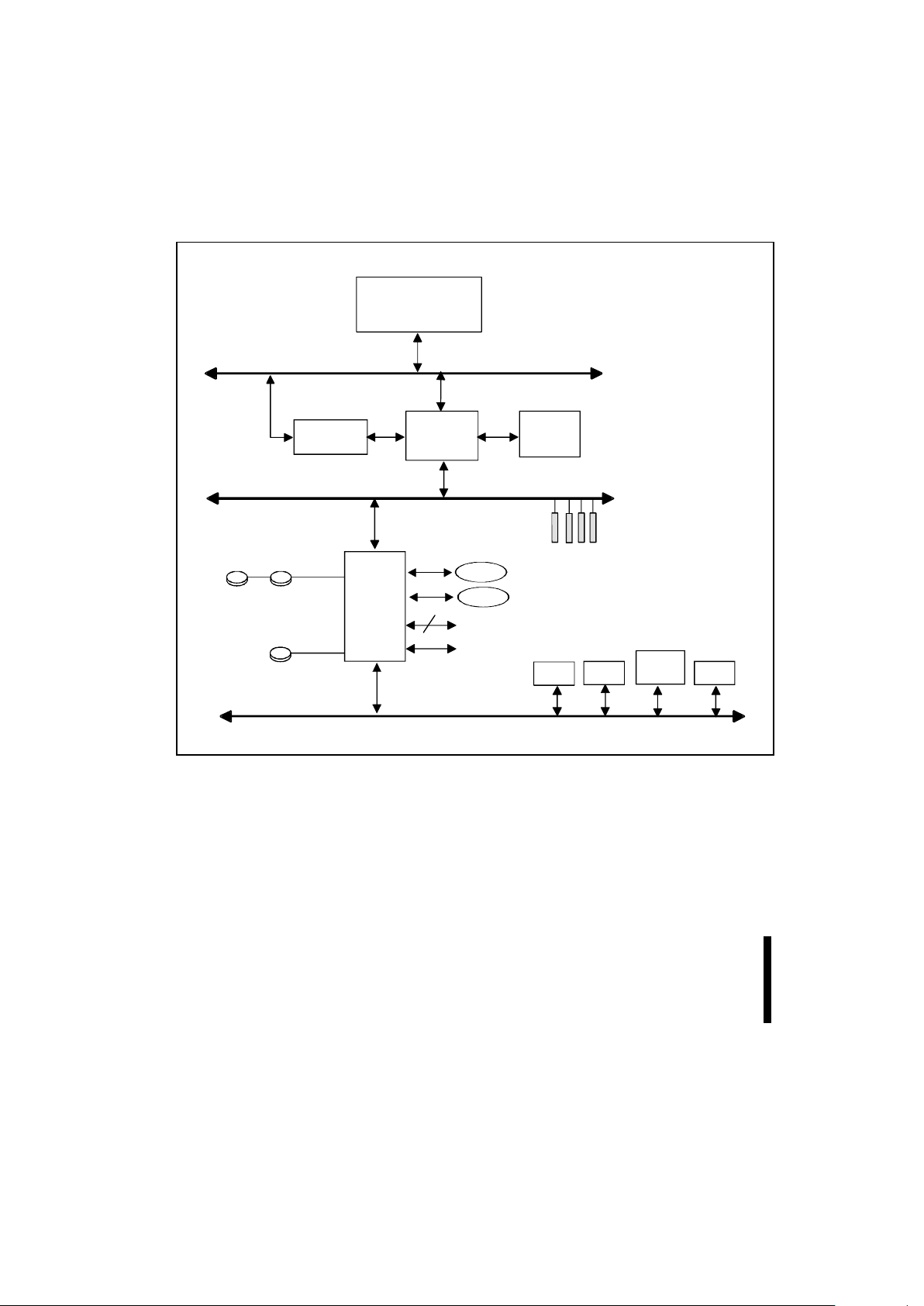
PIIX4 is a multi-function PCI device that integrates many system-level functions. Figure 1 shows an example
system block diagram using PIIX4.
PCI Bus (3.3V or 5V, 30/33 MHz)
Main
Memory
(DRAM)
Processor
Host Bus
Second Level
Cache
Host-to-PCI
Bridge
BMI IDE
Ultra DMA/33
CD ROM
Hard
Disk
ISA/EIO Bus
(3.3V; 5V Tolerant)
USB 2
USB 1
82371AB
(PIIX4)
GP[I,O] (30+)
SMBus
Audio
KBD
SP, PP,
FDC, IR
BIOS
PCI Slots
Hard
Disk
pix4_sys
Figure 1. PIIX4 System Block Diagram
PCI to ISA/EIO Bridge
PIIX4 is compatible with the PCI Rev 2.1 specification, as well as the IEEE 996 specification for the ISA (AT)
bus. On PCI, PIIX4 operates as a master for various internal modules, such as the USB controller, DMA
controller, IDE bus master controller, distributed DMA masters, and on behalf of ISA masters. PIIX4 operates as
a slave for its internal registers or for cycles that are passed to the ISA or EIO buses. All internal registers are
positively decoded.
Page 13

E 82371AB (PIIX4)
13
4/9/97 2:23 PM PIIX4aDS
INTEL CONFIDENTIAL
(until publication date)
PRELIMINARY
PIIX4 can be configured for a full ISA bus or a subset of the ISA bus called the Extended IO (EIO) bus. The use
of the EIO bus allows unused signals to be configured as general purpose inputs and outputs. PIIX4 can directly
drive up to five ISA slots without external data or address buffering. It also provides byte-swap logic, I/O
recovery support, wait-state generation, and SYSCLK generation. X-Bus chip selects are provided for Keyboard
Controller, BIOS, Real Time Clock, a second microcontroller, as well as two programmable chip selects.
PIIX4 can be configured as either a subtractive decode PCI to ISA bridge or as a positive decode bridge. This
gives a system designer the option of placing another subtractive decode bridge in the system (e.g., an Intel
380FB Dock Set).
IDE Interface (Bus Master capability and synchronous DMA Mode)
The fast IDE interface supports up to four IDE devices providing an interface for IDE hard disks and CD ROMs.
Each IDE device can have independent timings. The IDE interface supports PIO IDE transfers up to 14
Mbytes/sec and Bus Master IDE transfers up to 33 Mbytes/sec. It does not consume any ISA DMA resources.
The IDE interface integrates 16x32-bit buffers for optimal transfers.
PIIX4’s IDE system contains two independent IDE signal channels. They can be electrically isolated
independently, allowing for the implementation of a “glueless” Swap Bay. They can be configured to the standard
primary and secondary channels (four devices) or primary drive 0 and primary drive 1 channels (two devices).
This allows flexibility in system design and device power management.
Compatibility Modules (DMA Controller, Timer/Counters, Interrupt Controller)
The DMA controller incorporates the logic of two 82C37 DMA controllers, with seven independently
programmable channels. Channels [0:3] are hardwired to 8-bit, count-by-byte transfers, and channels [5:7] are
hardwired to 16-bit, count-by-word transfers. Any two of the seven DMA channels can be programmed to
support fast Type-F transfers. The DMA controller also generates the ISA refresh cycles.
The DMA controller supports two separate methods for handling legacy DMA via the PCI bus. The PC/PCI
protocol allows PCI-based peripherals to initiate DMA cycles by encoding requests and grants via three PC/PCI
REQ#/GNT# pairs. The second method, Distributed DMA, allows reads and writes to 82C37 registers to be
distributed to other PCI devices. The two methods can be enabled concurrently. The serial interrupt scheme
typically associated with Distributed DMA is also supported.
The timer/counter block contains three counters that are equivalent in function to those found in one 82C54
programmable interval timer. These three counters are combined to provide the system timer function, refresh
request, and speaker tone. The 14.31818-MHz oscillator input provides the clock source for these three
counters.
PIIX4 provides an ISA-Compatible interrupt controller that incorporates the functionality of two 82C59 interrupt
controllers. The two interrupt controllers are cascaded so that 14 external and two internal interrupts are
possible. In addition, PIIX4 supports a serial interrupt scheme. PIIX4 provides full support for the use of an
external IO APIC.
All of the registers in these modules can be read and restored. This is required to save and restore system state
after power has been removed and restored to the circuit.
Enhanced Universal Serial Bus (USB) Controller
The PIIX4 USB controller provides enhanced support for the Universal Host Controller Interface (UHCI). This
includes support that allows legacy software to use a USB-based keyboard and mouse.
Page 14

82371AB (PIIX4) E
14
4/9/97 2:23 PM PIIX4aDS
INTEL CONFIDENTIAL
(until publication date)
PRELIMINARY
RTC
PIIX4 contains a Motorola* MC146818A-compatible real-time clock with 256 bytes of battery-backed RAM. The
real-time clock performs two key functions: keeping track of the time of day and storing system data, even when
the system is powered down. The RTC operates on a 32.768-kHz crystal and a separate 3V lithium battery that
provides up to 7 years of protection.
The RTC also supports two lockable memory ranges. By setting bits in the configuration space, two 8-byte
ranges can be locked to read and write accesses. This prevents unauthorized reading of passwords or other
system security information.
The RTC also supports a date alarm, that allows for scheduling a wake up event up to 30 days in advance,
rather than just 24 hours in advance.
GPIO and Chip Selects
Various general purpose inputs and outputs are provided for custom system design. The number of inputs and
outputs varies depending on PIIX4 configuration. Two programmable chip selects are provided which allows the
designer to place devices on the X-Bus without the need for external decode logic.
Pentium
®
and Pentium® II Processor Interface
The PIIX4 CPU interface allows connection to all Pentium and Pentium II processors. The Sleep mode for the
Pentium II processors is also supported.
Enhanced Power Management
PIIX4’s power management functions include enhanced clock control, local and global monitoring support for 14
individual devices, and various low-power (suspend) states, such as Power-On Suspend, Suspend-to-DRAM,
and Suspend-to-Disk. A hardware-based thermal management circuit permits software-independent entrance to
low-power states. PIIX4 has dedicated pins to monitor various external events (e.g., interfaces to a notebook lid,
suspend/resume button, battery low indicators, etc.). PIIX4 contains full support for the Advanced Configuration
and Power Interface (ACPI) Specification.
System Management Bus (SMBus)
PIIX4 contains an SMBus Host interface that allows the CPU to communicate with SMBus slaves and an SMBus
Slave interface that allows external masters to activate power management events.
Configurability
PIIX4 provides a wide range of system configuration options. This includes full 16-bit I/O decode on internal
modules, dynamic disable on all the internal modules, various peripheral decode options, and many options on
system configuration.
Page 15

E 82371AB (PIIX4)
15
4/9/97 2:23 PM PIIX4aDS
INTEL CONFIDENTIAL
(until publication date)
PRELIMINARY
2.0. SIGNAL DESCRIPTION
This section provides a detailed description of each signal. The signals are arranged in functional groups
according to their associated interface.
The “#” symbol at the end of a signal name indicates that the active, or asserted state occurs when the signal is
at a low voltage level. When “#” is not present after the signal name, the signal is asserted when at the high
voltage level.
The terms assertion and negation are used exclusively. This is done to avoid confusion when working with a
mixture of “active low” and “active high” signal. The term assert, or assertion indicates that a signal is active,
independent of whether that level is represented by a high or low voltage. The term negate, or negation indicates
that a signal is inactive.
Certain signals have different functions, depending on the configuration programmed in the PCI configuration
space. The signal whose function is being described is in bold font. Some of the signals are multiplexed with
General Purpose Inputs and Outputs. The default configuration and control bits for each are described in Table 1
and Table 2.
Each output signal description includes the value of the signal During Reset, After Reset, and During POS.
During Reset refers to when the PCIRST# signal is asserted. After Reset is immediately after negation of
PCIRST# and the signal may change value anytime thereafter. The term High-Z means tri-stated. The term
Undefined means the signal could be high, low, tri-stated, or in some in-between level. Some of the power
management signals are reset with the RSMRST# input signal. The functionality of these signals during
RSMRST# assertion is described in the Suspend/Resume and Power Plane Control section.
The I/O buffer types are shown below:
Buffer Type Description
I input only signal
O totem pole output
I/O bi-direction, tri-state input/output pin
s/t/s sustained tri-state
OD open drain
I/OD input/open drain output is a standard input buffer with an open drain output
V This is not a standard signal. It is a power supply pin.
3.3V/2.5V Indicates the buffer is 3.3V or 2.5V only, depending on the voltage (3.3V or 2.5V) connected to
V
CCX pins.
3.3V/5V Indicates that the output is 3.3V and input is 3.3V receiver with 5V tolerance.
5V Indicates 3.3V receiver with 5V tolerance.
All 3V output signals can drive 5V TTL inputs. Most of the 3V input signals are 5V tolerant. The 3V input signals
which are powered via the RTC or Suspend power planes should not exceed their power supply voltage (see
Power Planes chapter for additional information). The open drain (OD) CPU interface signals should be pulled up
to the CPU interface signal voltage.
Page 16

82371AB (PIIX4) E
16
4/9/97 2:23 PM PIIX4aDS
INTEL CONFIDENTIAL
(until publication date)
PRELIMINARY
2.1. PIIX4 Signals
2.1.1. PCI BUS INTERFACE
Name Type Description
AD[31:0] I/O PCI ADDRESS/DATA. AD[31:0] is a multiplexed address and data bus. During the first
clock of a transaction, AD[31:0] contain a physical byte address (32 bits). During
subsequent clocks, AD[31:0] contain data.
A PIIX4 Bus transaction consists of an address phase followed by one or more data
phases. Little-endian byte ordering is used. AD[7:0] define the least significant byte
(LSB) and AD[31:24] the most significant byte (MSB).
When PIIX4 is a Target, AD[31:0] are inputs during the address phase of a transaction.
During the following data phase(s), PIIX4 may be asked to supply data on AD[31:0] for
a PCI read, or accept data for a PCI write.
As an Initiator, PIIX4 drives a valid address on AD[31:2] and 0 on AD[1:0] during the
address phase, and drives write or latches read data on AD[31:0] during the data
phase.
During Reset: High-Z After Reset: High-Z During POS: High-Z
C/BE#[3:0] I/O BUS COMMAND AND BYTE ENABLES. The command and byte enable signals are
multiplexed on the same PCI pins. During the address phase of a transaction,
C/BE[3:0]# define the bus command. During the data phase C/BE[3:0]# are used as
Byte Enables. The Byte Enables determine which byte lanes carry meaningful data.
C/BE0# applies to byte 0, C/BE1# to byte 1, etc. PIIX4 drives C/BE[3:0]# as an Initiator
and monitors C/BE[3:0]# as a Target.
During Reset: High-Z After Reset: High-Z During POS: High-Z
CLKRUN# I/O CLOCK RUN#. This signal is used to communicate to PCI peripherals that the PCI
clock will be stopped. Peripherals can assert CLKRUN# to request that the PCI clock
be restarted or to keep it from stopping. This function follows the protocol described in
the PCI Mobile Design Guide, Revision 1.0.
During Reset: Low After Reset: Low During POS: High
DEVSEL# I/O DEVICE SELECT. PIIX4 asserts DEVSEL# to claim a PCI transaction through positive
decoding or subtractive decoding (if enabled). As an output, PIIX4 asserts DEVSEL#
when it samples IDSEL active in configuration cycles to PIIX4 configuration registers.
PIIX4 also asserts DEVSEL# when an internal PIIX4 address is decoded or when PIIX4
subtractively or positively decodes a cycle for the ISA/EIO bus or IDE device. As an
input, DEVSEL# indicates the response to a PIIX4 initiated transaction and is also
sampled when deciding whether to subtractively decode the cycle. DEVSEL# is tristated from the leading edge of PCIRST#. DEVSEL# remains tri-stated until driven by
PIIX4 as a target.
During Reset: High-Z After Reset: High-Z During POS: High-Z
FRAME# I/O CYCLE FRAME. FRAME# is driven by the current Initiator to indicate the beginning and
duration of an access. While FRAME# is asserted data transfers continue. When
FRAME# is negated the transaction is in the final data phase. FRAME# is an input to
PIIX4 when it is the Target. FRAME# is an output when PIIX4 is the initiator. FRAME#
remains tri-stated until driven by PIIX4 as an Initiator.
During Reset: High-Z After Reset: High-Z During POS: High-Z
Page 17

E 82371AB (PIIX4)
17
4/9/97 2:23 PM PIIX4aDS
INTEL CONFIDENTIAL
(until publication date)
PRELIMINARY
Name Type Description
IDSEL I INITIALIZATION DEVICE SELECT. IDSEL is used as a chip select during PCI
configuration read and write cycles. PIIX4 samples IDSEL during the address phase of
a transaction. If IDSEL is sampled active, and the bus command is a configuration read
or write, PIIX4 responds by asserting DEVSEL# on the next cycle.
IRDY# I/O INITIATOR READY. IRDY# indicates PIIX4’s ability, as an Initiator, to complete the
current data phase of the transaction. It is used in conjunction with TRDY#. A data
phase is completed on any clock both IRDY# and TRDY# are sampled asserted. During
a write, IRDY# indicates PIIX4 has valid data present on AD[31:0]. During a read, it
indicates PIIX4 is prepared to latch data. IRDY# is an input to PIIX4 when PIIX4 is the
Target and an output when PIIX4 is an Initiator. IRDY# remains tri-stated until driven by
PIIX4 as a master.
During Reset: High-Z After Reset: High-Z During POS: High-Z
PAR O CALCULATED PARITY SIGNAL. PAR is “even” parity and is calculated on 36 bits;
AD[31:0] plus C/BE[3:0]#. “Even” parity means that the number of “1”s within the
36 bits plus PAR are counted and the sum is always even. PAR is always calculated on
36 bits regardless of the valid byte enables. PAR is generated for address and data
phases and is only guaranteed to be valid one PCI clock after the corresponding
address or data phase. PAR is driven and tri-stated identically to the AD[31:0] lines
except that PAR is delayed by exactly one PCI clock. PAR is an output during the
address phase (delayed one clock) for all PIIX4 initiated transactions. It is also an
output during the data phase (delayed one clock) when PIIX4 is the Initiator of a PCI
write transaction, and when it is the Target of a read transaction.
During Reset: High-Z After Reset: High-Z During POS: High-Z
PCIRST# O PCI RESET. PIIX4 asserts PCIRST# to reset devices that reside on the PCI bus. PIIX4
asserts PCIRST# during power-up and when a hard reset sequence is initiated through
the RC register. PCIRST# is driven inactive a minimum of 1 ms after PWROK is driven
active. PCIRST# is driven for a minimum of 1 ms when initiated through the RC register.
PCIRST# is driven asynchronously relative to PCICLK.
During Reset: Low After Reset: High During POS: High
PHOLD# O PCI HOLD. An active low assertion indicates that PIIX4 desires use of the PCI Bus.
Once the PCI arbiter has asserted PHLDA# to PIIX4, it may not negate it until PHOLD#
is negated by PIIX4. PIIX4 implements the passive release mechanism by toggling
PHOLD# inactive for one PCICLK.
During Reset: High-Z After Reset: High During POS: High
PHLDA# I PCI HOLD ACKNOWLEDGE. An active low assertion indicates that PIIX4 has been
granted use of the PCI Bus. Once PHLDA# is asserted, it cannot be negated unless
PHOLD# is negated first.
SERR# I/O SYSTEM ERROR. SERR# can be pulsed active by any PCI device that detects a
system error condition. Upon sampling SERR# active, PIIX4 can be programmed to
generate a non-maskable interrupt (NMI) to the CPU.
During Reset: High-Z After Reset: High-Z During POS: High-Z
Page 18

82371AB (PIIX4) E
18
4/9/97 2:23 PM PIIX4aDS
INTEL CONFIDENTIAL
(until publication date)
PRELIMINARY
Name Type Description
STOP# I/O STOP. STOP# indicates that PIIX4, as a Target, is requesting an initiator to stop the
current transaction. As an Initiator, STOP# causes PIIX4 to stop the current transaction.
STOP# is an output when PIIX4 is a Target and an input when PIIX4 is an Initiator.
STOP# is tri-stated from the leading edge of PCIRST#. STOP# remains tri-stated until
driven by PIIX4 as a slave.
During Reset: High-Z After Reset: High-Z During POS: High-Z
TRDY# I/O TARGET READY. TRDY# indicates PIIX4’s ability to complete the current data phase
of the transaction. TRDY# is used in conjunction with IRDY#. A data phase is
completed when both TRDY# and IRDY# are sampled asserted. During a read, TRDY#
indicates that PIIX4, as a Target, has place valid data on AD[31:0]. During a write, it
indicates PIIX4, as a Target is prepared to latch data. TRDY# is an input to PIIX4 when
PIIX4 is the Initiator and an output when PIIX4 is a Target. TRDY# is
tri-stated from the leading edge of PCIRST#. TRDY# remains tri-stated until driven
by PIIX4 as a slave.
During Reset: High-Z After Reset: High-Z During POS: High-Z
NOTES:
All of the signals in the host interface are described in the Pentium Processor data sheet. The preceding table
highlights PIIX4 specific uses of these signals.
2.1.2. ISA BUS INTERFACE
Name Type Description
AEN O ADDRESS ENABLE. AEN is asserted during DMA cycles to prevent I/O slaves from
misinterpreting DMA cycles as valid I/O cycles. When negated, AEN indicates that an
I/O slave may respond to address and I/O commands. When asserted, AEN informs
I/O resources on the ISA bus that a DMA transfer is occurring. This signal is also
driven high during PIIX4 initiated refresh cycles.
During Reset: High-Z After Reset: Low During POS: Low
BALE O BUS ADDRESS LATCH ENABLE. BALE is asserted by PIIX4 to indicate that the
address (SA[19:0], LA[23:17]) and SBHE# signal lines are valid. The LA[23:17]
address lines are latched on the trailing edge of BALE. BALE remains asserted
throughout DMA and ISA master cycles.
During Reset: High-Z After Reset: Low During POS: Low
IOCHK#/
GPI0
I I/O CHANNEL CHECK. IOCHK# can be driven by any resource on the ISA bus.
When asserted, it indicates that a parity or an uncorrectable error has occurred for
a device or memory on the ISA bus. A NMI will be generated to the CPU if the NMI
generation is enabled. If the EIO bus is used, this signal becomes a general purpose
input.
Page 19

E 82371AB (PIIX4)
19
4/9/97 2:23 PM PIIX4aDS
INTEL CONFIDENTIAL
(until publication date)
PRELIMINARY
Name Type Description
IOCHRDY I/O I/O CHANNEL READY. Resources on the ISA Bus negate IOCHRDY to indicate that
wait states are required to complete the cycle. This signal is normally high. IOCHRDY
is an input when PIIX4 owns the ISA Bus and the CPU or a PCI agent is accessing an
ISA slave, or during DMA transfers. IOCHRDY is output when an external ISA Bus
Master owns the ISA Bus and is accessing DRAM or a PIIX4 register. As a PIIX4
output, IOCHRDY is driven inactive (low) from the falling edge of the ISA commands.
After data is available for an ISA master read or PIIX4 latches the data for a write
cycle, IOCHRDY is asserted for 70 ns. After 70 ns, PIIX4 floats IOCHRDY. The 70 ns
includes both the drive time and the time it takes PIIX4 to float IOCHRDY. PIIX4 does
not drive this signal when an ISA Bus master is accessing an ISA Bus slave.
During Reset: High-Z After Reset: High-Z During POS: High-Z
IOCS16# I 16-BIT I/O CHIP SELECT. This signal is driven by I/O devices on the ISA Bus to
indicate support for 16-bit I/O bus cycles.
IOR# I/O I/O READ. IOR# is the command to an ISA I/O slave device that the slave may drive
data on to the ISA data bus (SD[15:0]). The I/O slave device must hold the data valid
until after IOR# is negated. IOR# is an output when PIIX4 owns the ISA Bus. IOR# is
an input when an external ISA master owns the ISA Bus.
During Reset: High-Z After Reset: High During POS: High
IOW# I/O I/O WRITE. IOW# is the command to an ISA I/O slave device that the slave may latch
data from the ISA data bus (SD[15:0]). IOW# is an output when PIIX4 owns the ISA
Bus. IOW# is an input when an external ISA master owns the ISA Bus.
During Reset: High-Z After Reset: High During POS: High
LA[23:17]/
GPO[7:1]
I/O ISA LA[23:17]. LA[23:17] address lines allow accesses to physical memory on the
ISA Bus up to 16 Mbytes. LA[23:17] are outputs when PIIX4 owns the ISA Bus. The
LA[23:17] lines become inputs whenever an ISA master owns the ISA Bus.
If the EIO bus is used, these signals become a general purpose output.
During Reset: High-Z After Reset: Undefined During POS: Last LA/GPO
MEMCS16# I/O MEMORY CHIP SELECT 16. MEMCS16# is a decode of LA[23:17] without any
qualification of the command signal lines. ISA slaves that are 16-bit memory devices
drive this signal low. PIIX4 ignores MEMCS16# during I/O access cycles and refresh
cycles. MEMCS16# is an input when PIIX4 owns the ISA Bus. PIIX4 drives this signal
low during ISA master to PCI memory cycles.
During Reset: High-Z After Reset: High-Z During POS: High-Z
MEMR# I/O MEMORY READ. MEMR# is the command to a memory slave that it may drive data
onto the ISA data bus. MEMR# is an output when PIIX4 is a master on the ISA Bus.
MEMR# is an input when an ISA master, other than PIIX4, owns the ISA Bus. This
signal is also driven by PIIX4 during refresh cycles. For DMA cycles, PIIX4, as a
master, asserts MEMR#.
During Reset: High-Z After Reset: High During POS: High
Page 20

82371AB (PIIX4) E
20
4/9/97 2:23 PM PIIX4aDS
INTEL CONFIDENTIAL
(until publication date)
PRELIMINARY
Name Type Description
MEMW# I/O MEMORY WRITE. MEMW# is the command to a memory slave that it may latch data
from the ISA data bus. MEMW# is an output when PIIX4 owns the ISA Bus. MEMW#
is an input when an ISA master, other than PIIX4, owns the ISA Bus. For DMA cycles,
PIIX4, as a master, asserts MEMW#.
During Reset: High-Z After Reset: High During POS: High
REFRESH# I/O REFRESH. As an output, REFRESH# is used by PIIX4 to indicate when a refresh
cycle is in progress. It should be used to enable the SA[7:0] address to the row
address inputs of all banks of dynamic memory on the ISA Bus. Thus, when MEMR#
is asserted, the entire expansion bus dynamic memory is refreshed. Memory slaves
must not drive any data onto the bus during refresh. As an output, this signal is driven
directly onto the ISA Bus. This signal is an output only when PIIX4 DMA refresh
controller is a master on the bus responding to an internally generated request for
refresh.
As an input, REFRESH# is driven by 16-bit ISA Bus masters to initiate refresh cycles.
During Reset: High-Z After Reset: High During POS: High
RSTDRV O RESET DRIVE. PIIX4 asserts RSTDRV to reset devices that reside on the ISA/EIO
Bus. PIIX4 asserts this signal during a hard reset and during power-up. RSTDRV is
asserted during power-up and negated after PWROK is driven active. RSTDRV is
also driven active for a minimum of 1 ms if a hard reset has been programmed in the
RC register.
During Reset: High After Reset: Low During POS: Low
SA[19:0] I/O SYSTEM ADDRESS[19:0]. These bi-directional address lines define the selection
with the granularity of 1 byte within the 1-Megabyte section of memory defined by the
LA[23:17] address lines. The address lines SA[19:17] that are coincident with
LA[19:17] are defined to have the same values as LA[19:17] for all memory cycles.
For I/O accesses, only SA[15:0] are used, and SA[19:16] are undefined. SA[19:0] are
outputs when PIIX4 owns the ISA Bus. SA[19:0] are inputs when an external ISA
Master owns the ISA Bus.
During Reset: High-Z After Reset: Undefined During POS: Last SA
SBHE# I/O SYSTEM BYTE HIGH ENABLE. SBHE# indicates, when asserted, that a byte is
being transferred on the upper byte (SD[15:8]) of the data bus. SBHE# is negated
during refresh cycles. SBHE# is an output when PIIX4 owns the ISA Bus. SBHE# is
an input when an external ISA master owns the ISA Bus.
During Reset: High-Z After Reset: Undefined During POS: High
SD[15:0] I/O SYSTEM DATA. SD[15:0] provide the 16-bit data path for devices residing on the ISA
Bus. SD[15:8] correspond to the high order byte and SD[7:0] correspond to the low
order byte. SD[15:0] are undefined during refresh.
During Reset: High-Z After Reset: Undefined During POS: High-Z
SMEMR# O STANDARD MEMORY READ. PIIX4 asserts SMEMR# to request an ISA memory
slave to drive data onto the data lines. If the access is below the 1-Mbyte range
(00000000h–000FFFFFh) during DMA compatible, PIIX4 master, or ISA master
cycles, PIIX4 asserts SMEMR#. SMEMR# is a delayed version of MEMR#.
During Reset: High-Z After Reset: High During POS: High
Page 21

E 82371AB (PIIX4)
21
4/9/97 2:23 PM PIIX4aDS
INTEL CONFIDENTIAL
(until publication date)
PRELIMINARY
Name Type Description
SMEMW# O STANDARD MEMORY WRITE. PIIX4 asserts SMEMW# to request an ISA memory
slave to accept data from the data lines. If the access is below the 1-Mbyte range
(00000000h–000FFFFFh) during DMA compatible, PIIX4 master, or ISA master
cycles, PIIX4 asserts SMEMW#. SMEMW# is a delayed version of MEMW#.
During Reset: High-Z After Reset: High During POS: High
ZEROWS# I ZERO WAIT STATES. An ISA slave asserts ZEROWS# after its address and
command signals have been decoded to indicate that the current cycle can be
shortened. A 16-bit ISA memory cycle can be reduced to two SYSCLKs. An 8-bit
memory or I/O cycle can be reduced to three SYSCLKs. ZEROWS# has no effect
during 16-bit I/O cycles.
If IOCHRDY is negated and ZEROWS# is asserted during the same clock, then
ZEROWS# is ignored and wait states are added as a function of IOCHRDY.
2.1.3. X-BUS INTERFACE
Name Type Description
A20GATE I ADDRESS 20 GATE. This input from the keyboard controller is logically combined with
bit 1 (FAST_A20) of the Port 92 Register, which is then output via the A20M# signal.
BIOSCS# O BIOS CHIP SELECT. This chip select is driven active during read or write accesses to
enabled BIOS memory ranges. BIOSCS# is driven combinatorially from the ISA
addresses SA[16:0] and LA[23:17], except during DMA cycles. During DMA cycles,
BIOSCS# is not generated.
During Reset: High After Reset: High During POS: High
KBCCS#/
GPO26
O KEYBOARD CONTROLLER CHIP SELECT. KBCCS# is asserted during I/O read or
write accesses to KBC locations 60h and 64h. It is driven combinatorially from the ISA
addresses SA[19:0] and LA[23:17].
If the keyboard controller does not require a separate chip select, this signal can be
programmed to a general purpose output.
During Reset: High After Reset: High During POS: High/GPO
MCCS# O MICROCONTROLLER CHIP SELECT. MCCS# is asserted during I/O read or write
accesses to IO locations 62h and 66h. It is driven combinatorially from the ISA
addresses SA[19:0] and LA[23:17].
During Reset: High After Reset: High During POS: High
PCS0#
PCS1#
O PROGRAMMABLE CHIP SELECTS. These active low chip selects are asserted for
ISA I/O cycles which are generated by PCI masters and which hit the programmable
I/O ranges defined in the Power Management section. The X-Bus buffer signals (XOE#
and XDIR#) are enabled while the chip select is active. (i.e., it is assumed that the
peripheral which is selected via this pin resides on the X-Bus.)
During Reset: High After Reset: High During POS: High
RCIN# I RESET CPU. This signal from the keyboard controller is used to generate an INIT
signal to the CPU.
Page 22

82371AB (PIIX4) E
22
4/9/97 2:23 PM PIIX4aDS
INTEL CONFIDENTIAL
(until publication date)
PRELIMINARY
Name Type Description
RTCALE/
GPO25
O REAL TIME CLOCK ADDRESS LATCH ENABLE. RTCALE is used to latch the
appropriate memory address into the RTC. A write to port 70h with the appropriate RTC
memory address that will be written to or read from causes RTCALE to be asserted.
RTCALE is asserted on falling IOW# and remains asserted for two SYSCLKs.
If the internal Real Time Clock is used, this signal can be programmed as a general
purpose output.
During Reset: Low After Reset: Low During POS: Low/GPO
RTCCS#/
GPO24
O REAL TIME CLOCK CHIP SELECT. RTCCS# is asserted during read or write I/O
accesses to RTC location 71h. RTCCS# can be tied to a pair of external OR gates to
generate the real time clock read and write command signals. If the internal Real Time
Clock is used, this signal can be programmed as a general purpose output.
During Reset: High After Reset: High During POS: High/GPO
XDIR#/
GPO22
O X-BUS TRANSCEIVER DIRECTION. XDIR# is tied directly to the direction control of a
74’245 that buffers the X-Bus data, XD[7:0]. XDIR# is asserted (driven low) for all I/O
read cycles regardless if the accesses is to a PIIX4 supported device. XDIR# is
asserted for memory cycles only if BIOS or APIC space has been decoded. For PCI
master initiated read cycles, XDIR# is asserted from the falling edge of either IOR# or
MEMR# (from MEMR# only if BIOS or APIC space has been decoded), depending on
the cycle type. For ISA master-initiated read cycles, XDIR# is asserted from the falling
edge of either IOR# or MEMR# (from MEMR# only if BIOS space has been decoded),
depending on the cycle type. When the rising edge of IOR# or MEMR# occurs, PIIX4
negates XDIR#. For DMA read cycles from the X-Bus, XDIR# is driven low from
DACKx# falling and negated from DACKx# rising. At all other times, XDIR# is negated
high.
If the X-Bus not used, then this signal can be programmed to be a general purpose
output.
During Reset: High After Reset: High During POS: High/GPO
XOE#/
GPO23
O X-BUS TRANSCEIVER OUTPUT ENABLE. XOE# is tied directly to the output enable
of a 74’245 that buffers the X-Bus data, XD[7:0], from the system data bus, SD[7:0].
XOE# is asserted anytime a PIIX4 supported X-Bus device is decoded, and the devices
decode is enabled in the X-Bus Chip Select Enable Register (BIOSCS#, KBCCS#,
RTCCS#, MCCS#) or the Device Resource B (PCCS0#) and Device Resource C
(PCCS1#). XOE# is asserted from the falling edge of the ISA commands (IOR#, IOW#,
MEMR#, or MEMW#) for PCI Master and ISA master-initiated cycles. XOE# is negated
from the rising edge of the ISA command signals for PCI Master initiated cycles and the
SA[16:0] and LA[23:17] address for ISA master-initiated cycles. XOE# is not generated
during any access to an X-Bus peripheral in which its decode space has been disabled.
If an X-Bus not used, then this signal can be programmed to be a general purpose
output.
During Reset: High After Reset: High During POS: High/GPO
Page 23

E 82371AB (PIIX4)
23
4/9/97 2:23 PM PIIX4aDS
INTEL CONFIDENTIAL
(until publication date)
PRELIMINARY
2.1.4. DMA SIGNALS
Name Type Description
DACK[0,1,2,3]#
DACK[5,6,7]#
O DMA ACKNOWLEDGE. The DACK# output lines indicate that a request for DMA
service has been granted by PIIX4 or that a 16-bit master has been granted the
bus. The active level (high or low) is programmed via the DMA Command
Register. These lines should be used to decode the DMA slave device with the
IOR# or IOW# line to indicate selection. If used to signal acceptance of a bus
master request, this signal indicates when it is legal to assert MASTER#. If the
DREQ goes inactive prior to DACK# being asserted,
the DACK# signal will not be asserted.
During Reset: High After Reset: High During POS: High
DREQ[0,1,2,3]
DREQ[5,6,7]
I DMA REQUEST. The DREQ lines are used to request DMA service from PIIX4’s
DMA controller or for a 16-bit master to gain control of the ISA expansion bus. The
active level (high or low) is programmed via the DMA Command Register. All
inactive to active edges of DREQ are assumed to be asynchronous. The request
must remain active until the appropriate DACKx# signal is asserted.
REQ[A:C]#/
GPI[2:4]
I PC/PCI DMA REQUEST. These signals are the DMA requests for PC/PCI
protocol. They are used by a PCI agent to request DMA services and follow the
PCI Expansion Channel Passing protocol as defined in the PCI DMA section.
If the PC/PCI request is not needed, these pins can be used as general-purpose
inputs.
GNT[A:C]#/
GPO[9:11]
O PC/PCI DMA ACKNOWLEDGE. These signals are the DMA grants for PC/PCI
protocol. They are used by a PIIX4 to acknowledge DMA services and follow the
PCI Expansion Channel Passing protocol as defined in the PCI DMA section.
If the PC/PCI request is not needed, these pins can be used as general-purpose
outputs.
During Reset: High After Reset: High During POS: High/GPO
TC O TERMINAL COUNT. PIIX4 asserts TC to DMA slaves as a terminal count
indicator. PIIX4 asserts TC after a new address has been output, if the byte count
expires with that transfer. TC remains asserted until AEN is negated, unless AEN
is negated during an autoinitialization. TC is negated before AEN is negated during
an autoinitialization.
During Reset: Low After Reset: Low During POS: Low
Page 24

82371AB (PIIX4) E
24
4/9/97 2:23 PM PIIX4aDS
INTEL CONFIDENTIAL
(until publication date)
PRELIMINARY
2.1.5. INTERRUPT CONTROLLER/APIC SIGNALS
Name Type Description
APICACK#/
GPO12
O APIC ACKNOWLEDGE. This active low output signal is asserted by PIIX4 after its
internal buffers are flushed in response to the APICREQ# signal. When the I/O APIC
samples this signal asserted it knows that PIIX4’s buffers are flushed and that it can
proceed to send the APIC interrupt. The APICACK# output is synchronous to
PCICLK.
If the external APIC is not used, then this is a general-purpose output.
During Reset: High After Reset: High During POS: High/GPO
APICCS#/
GPO13
O APIC CHIP SELECT. This active low output signal is asserted when the APIC Chip
Select is enabled and a PCI originated cycle is positively decoded within the
programmed I/O APIC address space.
If the external APIC is not used, this pin is a general-purpose output.
During Reset: High After Reset: High During POS: High/GPO
APICREQ#/
GPI5
I APIC REQUEST. This active low input signal is asserted by an external APIC
device prior to sending an interrupt over the APIC serial bus. When PIIX4 samples
this pin active it will flush its F-type DMA buffers pointing towards PCI. Once the
buffers are flushed, PIIX4 asserts APICACK# which indicates to the external APIC
that it can proceed to send the APIC interrupt. The APICREQ# input must be
synchronous to PCICLK.
If the external APIC is not used, this pin is a general-purpose input.
INTR OD INTERRUPT. See CPU Interface Signals.
IRQ0/
GPO14
O INTERRUPT REQUEST 0. This output reflects the state of the internal IRQ0 signal
from the system timer.
If the external APIC is not used, this pin is a general-purpose output.
During Reset: Low After Reset: Low During POS: IRQ0/GPO
IRQ1 I INTERRUPT REQUEST 1. IRQ1 is always edge triggered and can not be modified
by software to level sensitive. A low to high transition on IRQ1 is latched by PIIX4.
IRQ1 must remain asserted until after the interrupt is acknowledged. If the input goes
inactive before this time, a default IRQ7 is reported in response to the interrupt
acknowledge cycle.
Page 25

E 82371AB (PIIX4)
25
4/9/97 2:23 PM PIIX4aDS
INTEL CONFIDENTIAL
(until publication date)
PRELIMINARY
Name Type Description
IRQ 3:7, 9:11,
14:15
I INTERRUPT REQUESTS 3:7, 9:11, 14:15. The IRQ signals provide both system
board components and ISA Bus I/O devices with a mechanism for asynchronously
interrupting the CPU. These interrupts may be programmed for either an edge
sensitive or a high level sensitive assertion mode. Edge sensitive is the default
configuration.
An active IRQ input must remain asserted until after the interrupt is acknowledged. If
the input goes inactive before this time, a default IRQ7 is reported in response to the
interrupt acknowledge cycle.
IRQ8#/
GPI6
I/O IRQ 8#. IRQ8# is always an active low edge triggered interrupt and can not be
modified by software.
IRQ8# must remain asserted until after the interrupt is acknowledged. If the input
goes inactive before this time, a default IRQ7 is reported in response to the interrupt
acknowledge cycle.
If using the internal RTC, then this can be programmed as a general-purpose input. If
enabling an APIC, this signal becomes an output and must not be programmed as a
general purpose input.
IRQ9OUT#/
GPO29
O IRQ9OUT#. IRQ9OUT# is used to route the internally generated SCI and SMBus
interrupts out of the PIIX4 for connection to an external IO APIC. If APIC is disabled,
this signal pin is a General Purpose Output.
During Reset: High After Reset: High During POS: IRQ9OUT#/GPO
IRQ 12/M I INTERRUPT REQUEST 12. In addition to providing the standard interrupt function
as described in the pin description for IRQ[3:7,9:11,14:15], this pin can also be
programmed to provide the mouse interrupt function.
When the mouse interrupt function is selected, a low to high transition on this signal
is latched by PIIX4 and an INTR is generated to the CPU as IRQ12. An internal
IRQ12 interrupt continues to be generated until a Reset or an I/O read access to
address 60h (falling edge of IOR#) is detected.
PIRQ[A:D]# I/OD
PCI
PROGRAMMABLE INTERRUPT REQUEST. The PIRQx# signals are active low,
level sensitive, shareable interrupt inputs. They can be individually steered to ISA
interrupts IRQ [3:7,9:12,14:15]. The USB controller uses PIRQD# as its output
signal.
SERIRQ/
GPI7
I/O SERIAL INTERRUPT REQUEST. Serial interrupt input decoder, typically used in
conjunction with the Distributed DMA protocol.
If not using serial interrupts, this pin can be used as a general-purpose input.
Page 26

82371AB (PIIX4) E
26
4/9/97 2:23 PM PIIX4aDS
INTEL CONFIDENTIAL
(until publication date)
PRELIMINARY
2.1.6. CPU INTERFACE SIGNALS
Name Type Description
A20M# OD ADDRESS 20 MASK. PIIX4 asserts A20M# to the CPU based on combination of Port
92 Register, bit 1 (FAST_A20), and A20GATE input signal.
During Reset: High-Z After Reset: High-Z During POS: High-Z
CPURST OD CPU RESET. PIIX4 asserts CPURST to reset the CPU. PIIX4 asserts CPURST during
power-up and when a hard reset sequence is initiated through the RC register.
CPURST is driven inactive a minimum of 2 ms after PWROK is driven active. CPURST
is driven active for a minimum of 2 ms when initiated through the RC register. The
inactive edge of CPURST is driven synchronously to the rising edge of PCICLK. If a
hard reset is initiated through the RC register, PIIX4 resets its internal registers (in both
core and suspend wells) to their default state.
This signal is active high for Pentium processor and active-low for Pentium II processor
as determined by CONFIG1 signal.
For values During Reset, After Reset, and During POS, see the Suspend/Resume
and Resume Control Signaling section.
FERR# I NUMERIC COPROCESSOR ERROR. This pin functions as a FERR# signal supporting
coprocessor errors. This signal is tied to the coprocessor error signal on the CPU. If
FERR# is asserted, PIIX4 generates an internal IRQ13 to its interrupt controller unit.
PIIX4 then asserts the INT output to the CPU. FERR# is also used to gate the IGNNE#
signal to ensure that IGNNE# is not asserted to the CPU unless FERR# is active.
IGNNE# OD IGNORE NUMERIC EXCEPTION. This signal is connected to the ignore numeric
exception pin on the CPU. IGNNE# is only used if the PIIX4 coprocessor error reporting
function is enabled. If FERR# is active, indicating a coprocessor error,
a write to the Coprocessor Error Register (F0h) causes the IGNNE# to be asserted.
IGNNE# remains asserted until FERR# is negated. If FERR# is not asserted when the
Coprocessor Error Register is written, the IGNNE# signal is not asserted.
During Reset: High-Z After Reset: High-Z During POS: High-Z
INIT OD INITIALIZATION. INIT is asserted in response to any one of the following conditions.
When the System Reset bit in the Reset Control Register is reset to 0 and the Reset
CPU bit toggles from 0 to 1, PIIX4 initiates a soft reset by asserting INIT. PIIX4 also
asserts INIT if a Shut Down Special cycle is decoded on the PCI Bus, if the RCIN#
signal is asserted, or if a write occurs to Port 92h, bit 0. When asserted, INIT remains
asserted for approximately 64 PCI clocks before being negated.
This signal is active high for Pentium processor and active-low for Pentium II processor
as determined by CONFIG1 signal.
Pentium Processor:
During Reset: Low After Reset: Low During POS: Low
Pentium II Processor:
During Reset: High After Reset: High During POS: High
INTR OD CPU INTERRUPT. INTR is driven by PIIX4 to signal the CPU that an interrupt request
is pending and needs to be serviced. It is asynchronous with respect to SYSCLK or
PCICLK and is always an output. The interrupt controller must be programmed following
PCIRST# to ensure that INTR is at a known state.
During Reset: Low After Reset: Low During POS: Low
Page 27

E 82371AB (PIIX4)
27
4/9/97 2:23 PM PIIX4aDS
INTEL CONFIDENTIAL
(until publication date)
PRELIMINARY
Name Type Description
NMI OD NON-MASKABLE INTERRUPT. NMI is used to force a nonmaskable interrupt to the
CPU. PIIX4 generates an NMI when either SERR# or IOCHK# is asserted, depending
on how the NMI Status and Control Register is programmed. The CPU detects an NMI
when it detects a rising edge on NMI. After the NMI interrupt routine processes the
interrupt, the NMI status bits in the NMI Status and Control Register are cleared by
software. The NMI interrupt routine must read this register to determine the source of
the interrupt. The NMI is reset by setting the corresponding NMI source enable/disable
bit in the NMI Status and Control Register. To enable NMI interrupts, the two NMI
enable/disable bits in the register must be set to 0, and the NMI mask bit in the NMI
Enable/Disable and Real Time Clock Address Register must be set to 0. Upon
PCIRST#, this signal is driven low.
During Reset: Low After Reset: Low During POS: Low
SLP# OD SLEEP. This signal is output to the Pentium II processor in order to put it into Sleep
state. For Pentium processor it is a No Connect.
During Reset: High-Z After Reset: High-Z During POS: High-Z
SMI# OD SYSTEM MANAGEMENT INTERRUPT. SMI# is an active low synchronous output that
is asserted by PIIX4 in response to one of many enabled hardware or software events.
The CPU recognizes the falling edge of SMI# as the highest priority interrupt in the
system, with the exception of INIT, CPURST, and FLUSH.
During Reset: High-Z After Reset: High-Z During POS: High-Z
STPCLK# OD STOP CLOCK. STPCLK# is an active low synchronous output that is asserted by PIIX4
in response to one of many hardware or software events. STPCLK# connects directly to
the CPU and is synchronous to PCICLK.
During Reset: High-Z After Reset: High-Z During POS: High-Z
Page 28

82371AB (PIIX4) E
28
4/9/97 2:23 PM PIIX4aDS
INTEL CONFIDENTIAL
(until publication date)
PRELIMINARY
2.1.7. CLOCKING SIGNALS
Name Type Description
CLK48 I 48-MHZ CLOCK. 48-MHz clock used by the internal USB host controller. This signal
may be stopped during suspend modes.
PCICLK I FREE-RUNNING PCI CLOCK. A clock signal running at 30 or 33 MHz, PCICLK
provides timing for all transactions on the PCI Bus. All other PCI signals are sampled on
the rising edge of PCICLK, and all timing parameters are defined with respect to this
edge. Because many of the circuits in PIIX4 run off the PCI clock, this signal MUST be
kept active, even if the PCI bus clock is not active.
OSC I 14.31818-MHZ CLOCK. Clock signal used by the internal 8254 timer. This clock signal
may be stopped during suspend modes.
RTCX1,
RTCX2
I/O RTC CRYSTAL INPUTS: These connected directly to a 32.768-kHz crystal. External
capacitors are required. These clock inputs are required even if the internal RTC is not
being used.
SUSCLK O SUSPEND CLOCK. 32.768-kHz output clock provided to the Host-to-PCI bridge used
for maintenance of DRAM refresh. This signal is stopped during Suspend-to-Disk and
Soft Off modes. For values During Reset, After Reset, and During POS, see the
Suspend/Resume and Resume Control Signaling section.
SYSCLK O ISA SYSTEM CLOCK. SYSCLK is the reference clock for the ISA bus. It drives the ISA
bus directly. The SYSCLK is generated by dividing PCICLK by 4. The SYSCLK
frequencies supported are 7.5 MHz and 8.33 MHz. For PCI accesses to the ISA bus,
SYSCLK may be stretched low to synchronize BALE falling to the rising edge of
SYSCLK.
During Reset: Running After Reset: Running During POS: Low
2.1.8. IDE SIGNALS
Name Type Description
PDA[2:0] O PRIMARY DISK ADDRESS[2:0]. These signals indicate which byte in either the ATA
command block or control block is being addressed.
If the IDE signals are configured for Primary and Secondary, these signals are
connected to the corresponding signals on the Primary IDE connector.
If the IDE signals are configured for Primary 0 and Primary 1, these signals are used for
the Primary 0 connector.
During Reset: High-Z After Reset: Undefined
1
During POS: PDA
PDCS1# O PRIMARY DISK CHIP SELECT FOR 1F0H−−1F7H RANGE. For ATA command register
block. If the IDE signals are configured for Primary and Secondary, this output signal is
connected to the corresponding signal on the Primary IDE connector.
If the IDE signals are configured for Primary Master and Primary Slave, this signal is
used for the Primary Master connector.
During Reset: High After Reset: High During POS: High
Page 29

E 82371AB (PIIX4)
29
4/9/97 2:23 PM PIIX4aDS
INTEL CONFIDENTIAL
(until publication date)
PRELIMINARY
Name Type Description
PDCS3# O PRIMARY DISK CHIP SELECT FOR 3F0−−3F7 RANGE. For ATA control register block.
If the IDE signals are configured for Primary and Secondary, this output signal is
connected to the corresponding signal on the Primary IDE connector.
If the IDE signals are configured for Primary Master and Primary Slave, this signal is
used for the Primary Master connector.
During Reset: High After Reset: High During POS: High
PDD[15:0] I/O PRIMARY DISK DATA[15:0]. These signals are used to transfer data to or from the IDE
device. If the IDE signals are configured for Primary and Secondary, these signals are
connected to the corresponding signals on the Primary IDE connector.
If the IDE signals are configured for Primary Master and Primary Slave, this signal is
used for the Primary Master connector.
During Reset: High-Z After Reset: Undefined
1
During POS: PDD
PDDACK# O PRIMARY DMA ACKNOWLEDGE. This signal directly drives the IDE device DMACK#
signal. It is asserted by PIIX4 to indicate to IDE DMA slave devices that a given data
transfer cycle (assertion of PDIOR# or PDIOW#) is a DMA data transfer cycle. This
signal is used in conjunction with the PCI bus master IDE function. It is not associated
with any AT compatible DMA channel.
If the IDE signals are configured for Primary and Secondary, this signal is connected to
the corresponding signal on the Primary IDE connector.
If the IDE signals are configured for Primary Master and Primary Slave, this signal is
used for the Primary Master connector.
During Reset: High After Reset: High During POS: High
PDDREQ I PRIMARY DISK DMA REQUEST. This input signal is directly driven from the IDE
device DMARQ signal. It is asserted by the IDE device to request a data transfer, and
used in conjunction with the PCI bus master IDE function. It is not associated with any
AT compatible DMA channel.
If the IDE signals are configured for Primary and Secondary, this signal is connected to
the corresponding signal on the Primary IDE connector.
If the IDE signals are configured for Primary Master and Primary Slave, this signal is
used for the Primary Master connector.
Page 30

82371AB (PIIX4) E
30
4/9/97 2:23 PM PIIX4aDS
INTEL CONFIDENTIAL
(until publication date)
PRELIMINARY
Name Type Description
PDIOR# O PRIMARY DISK IO READ. In normal IDE this is the command to the IDE device that it
may drive data onto the PDD[15:0] lines. Data is latched by PIIX4 on the negation edge
of PDIOR#. The IDE device is selected either by the ATA register file chip selects
(PDCS1#, PDCS3#) and the PDA[2:0] lines, or the IDE DMA slave arbitration signals
(PDDACK#).
In an Ultra DMA/33 read cycle, this signal is used as DMARDY# which is negated by the
PIIX4 to pause Ultra DMA/33 transfers. In an Ultra DMA/33 write cycle, this signal is
used as the STROBE signal, with the drive latching data on rising and falling edges of
STROBE.
If the IDE signals are configured for Primary and Secondary, this signal is connected to
the corresponding signal on the Primary IDE connector.
If the IDE signals are configured for Primary Master and Primary Slave, this signal is
used for the Primary Master connector.
During Reset: High After Reset: High During POS: High
PDIOW# O PRIMARY DISK IO WRITE. In normal IDE mode, this is the command to the IDE device
that it may latch data from the PDD[15:0] lines. Data is latched by the IDE device on the
negation edge of PDIOW#. The IDE device is selected either by the ATA register file
chip selects (PDCS1#, PDCS3#) and the PDA[2:0] lines, or the IDE DMA slave
arbitration signals (PDDACK#).
For Ultra DMA/33 mode, this signal is used as the STOP signal, which is used to
terminate an Ultra DMA/33 transaction. If the IDE signals are configured for Primary and
Secondary, this signal is connected to the corresponding signal on the Primary IDE
connector.
If the IDE signals are configured for Primary Master and Primary Slave, this signal is
used for the Primary Master connector.
During Reset: High After Reset: High During POS: High-Z
PIORDY I PRIMARY IO CHANNEL READY. In normal IDE mode, this input signal is directly
driven by the corresponding IDE device IORDY signal.
In an Ultra DMA/33 read cycle, this signal is used as STROBE, with the PIIX4 latching
data on rising and falling edges of STROBE. In an Ultra DMA/33 write cycle, this signal
is used as the DMARDY# signal which is negated by the drive to pause Ultra DMA/33
transfers.
If the IDE signals are configured for Primary and Secondary, this signal is connected to
the corresponding signal on the Primary IDE connector.
If the IDE signals are configured for Primary Master and Primary Slave, this signal is
used for the Primary Master connector.
This is a Schmitt triggered input.
Page 31

E 82371AB (PIIX4)
31
4/9/97 2:23 PM PIIX4aDS
INTEL CONFIDENTIAL
(until publication date)
PRELIMINARY
Name Type Description
SDA[2:0] O SECONDARY DISK ADDRESS[2:0]. These signals indicate which byte in either the
ATA command block or control block is being addressed. If the IDE signals are
configured for Primary and Secondary, these signals are connected to the
corresponding signals on the Secondary IDE connector.
If the IDE signals are configured for Primary Master and Primary Slave, these signals
are used for the Primary Slave connector.
During Reset: High-Z After Reset: Undefined
1
During POS: SDA
SDCS1# O SECONDARY CHIP SELECT FOR 170H−−177H RANGE. For ATA command register
block. If the IDE signals are configured for Primary and Secondary, this output signal is
connected to the corresponding signal on the Secondary IDE connector.
If the IDE signals are configured for Primary Master and Primary Slave, these signals
are used for the Primary Slave connector.
During Reset: High After Reset: High During POS: High
SDCS3# O SECONDARY CHIP SELECT FOR 370H−−377H RANGE. For ATA control register
block. If the IDE signals are configured for Primary and Secondary, this output signal is
connected to the corresponding signal on the Secondary IDE connector.
If the IDE signals are configured for Primary Master and Primary Slave, these signals
are used for the Primary Slave connector.
During Reset: High After Reset: High During POS: High-Z
SDD[15:0] I/O SECONDARY DISK DATA[15:0]. These signals are used to transfer data to or from the
IDE device. If the IDE signals are configured for Primary and Secondary, these signals
are connected to the corresponding signals on the Secondary IDE connector.
If the IDE signals are configured for Primary Master and Primary Slave, these signals
are used for the Primary Slave connector.
During Reset: High-Z After Reset: Undefined
1
During POS: SDD
SDDACK# O SECONDARY DMA ACKNOWLEDGE. This signal directly drives the IDE device
DMACK# signal. It is asserted by PIIX4 to indicate to IDE DMA slave devices that a
given data transfer cycle (assertion of SDIOR# or SDIOW#) is a DMA data transfer
cycle. This signal is used in conjunction with the PCI bus master IDE function. It is not
associated with any AT compatible DMA channel.
If the IDE signals are configured for Primary and Secondary, this signal is connected to
the corresponding signal on the Secondary IDE connector.
If the IDE signals are configured for Primary Master and Primary Slave, these signals
are used for the Primary Slave connector.
During Reset: High After Reset: High During POS: High
Page 32

82371AB (PIIX4) E
32
4/9/97 2:23 PM PIIX4aDS
INTEL CONFIDENTIAL
(until publication date)
PRELIMINARY
Name Type Description
SDDREQ I SECONDARY DISK DMA REQUEST. This input signal is directly driven from the IDE
device DMARQ signal. It is asserted by the IDE device to request a data transfer, and
used in conjunction with the PCI bus master IDE function. It is not associated with any
AT compatible DMA channel.
If the IDE signals are configured for Primary and Secondary, this signal is connected to
the corresponding signal on the Secondary IDE connector.
If the IDE signals are configured for Primary Master and Primary Slave, these signals
are used for the Primary Slave connector.
SDIOR# O SECONDARY DISK IO READ. In normal IDE mode, this is the command to the IDE
device that it may drive data onto the SDD[15:0] lines. Data is latched by the PIIX4 on
the negation edge of SDIOR#. The IDE device is selected either by the ATA register file
chip selects (SDCS1#, SDCS3#) and the SDA[2:0] lines, or the IDE DMA slave
arbitration signals (SDDACK#).
In an Ultra DMA/33 read cycle, this signal is used as DMARDY# which is negated by the
PIIX4 to pause Ultra DMA/33 transfers. In an Ultra DMA/33 write cycle, this signal is
used as the STROBE signal, with the drive latching data on rising and falling edges of
STROBE.
If the IDE signals are configured for Primary and Secondary, this signal is connected to
the corresponding signal on the Secondary IDE connector.
If the IDE signals are configured for Primary Master and Primary Slave, these signals
are used for the Primary Slave connector.
During Reset: High After Reset: High During POS: High
SDIOW# O SECONDARY DISK IO WRITE. In normal IDE mode, this is the command to the IDE
device that it may latch data from the SDD[15:0] lines. Data is latched by the IDE device
on the negation edge of SDIOW#. The IDE device is selected either by the ATA register
file chip selects (SDCS1#, SDCS3#) and the SDA[2:0] lines, or the IDE DMA slave
arbitration signals (SDDACK#).
In read and write cycles this signal is used as the STOP signal, which is used to
terminate an Ultra DMA/33 transaction.
If the IDE signals are configured for Primary and Secondary, this signal is connected to
the corresponding signal on the Secondary IDE connector.
If the IDE signals are configured for Primary Master and Primary Slave, these signals
are used for the Primary Slave connector.
During Reset: High After Reset: High During POS: High
Page 33

E 82371AB (PIIX4)
33
4/9/97 2:23 PM PIIX4aDS
INTEL CONFIDENTIAL
(until publication date)
PRELIMINARY
Name Type Description
SIORDY I SECONDARY IO CHANNEL READY. In normal IDE mode, this input signal is directly
driven by the corresponding IDE device IORDY signal.
In an Ultra DMA/33 read cycle, this signal is used as STROBE, with the PIIX4 latching
data on rising and falling edges of STROBE. In an Ultra DMA write cycle, this signal is
used as the DMARDY# signal which is negated by the drive to pause Ultra DMA/33
transfers.
If the IDE signals are configured for Primary and Secondary, this signal is connected to
the corresponding signal on the Secondary IDE connector.
If the IDE signals are configured for Primary Master and Primary Slave, these signals
are used for the Primary Slave connector.
This is a Schmitt triggered input.
NOTES:
1. After reset, all undefined signals on the primary channel will default to the same values as the undefined
signals on the secondary channel.
2.1.9. UNIVERSAL SERIAL BUS SIGNALS
Name Type Description
OC[1:0]# I OVER CURRENT DETECT. These signals are used to monitor the status of the USB
power supply lines. The corresponding USB port is disabled when its over current signal
is asserted.
USBP0+,
USBP0–
I/O SERIAL BUS PORT 0. This signal pair comprises the differential data signal for USB
port 0.
During Reset: High-Z After Reset: High-Z During POS: High-Z
USBP1+,
USBP1–
I/O SERIAL BUS PORT 1. This signal pair comprises the differential data signal for USB
port 1.
During Reset: High-Z After Reset: High-Z During POS: High-Z
2.1.10. POWER MANAGEMENT SIGNALS
Name Type Description
BATLOW#/
GPI9
I BATTERY LOW. Indicates that battery power is low. PIIX4 can be programmed to
prevent a resume operation when the BATLOW# signal is asserted.
If the Battery Low function is not needed, this pin can be used as a general-purpose
input.
CPU_STP#/
GPO17
O CPU CLOCK STOP. Active low control signal to the clock generator used to disable
the CPU clock outputs. If this function is not needed, then this signal can be used as
a general-purpose output.
For values During Reset, After Reset, and During POS, see the Suspend/Resume
and Resume Control Signaling section.
Page 34

82371AB (PIIX4) E
34
4/9/97 2:23 PM PIIX4aDS
INTEL CONFIDENTIAL
(until publication date)
PRELIMINARY
Name Type Description
EXTSMI# I/OD EXTERNAL SYSTEM MANAGEMENT INTERRUPT. EXTSMI# is a falling edge
triggered input to PIIX4 indicating that an external device is requesting the system to
enter SMM mode. When enabled, a falling edge on EXTSMI# results in the assertion
of the SMI# signal to the CPU. EXTSMI# is an asynchronous input to PIIX4.
However, when the setup and hold times are met, it is only required to be asserted
for one PCICLK. Once negated EXTSMI# must remain negated for at least four
PCICLKs to allow the edge detect logic to reset. EXTSMI# is asserted by PIIX4 in
response to SMI# being activated within the Serial IRQ function. An external pull-up
should be placed on this signal.
LID/
GPI10
I LID INPUT. This signal can be used to monitor the opening and closing of the
display lid of a notebook computer. It can be used to detect both low to high
transition or a high to low transition and these transitions will generate an SMI# if
enabled. This input contains logic to perform a 16-ms debounce of the input signal. If
the LID function is not needed, this pin can be used as a general-purpose input.
PCIREQ[A:D]# I PCI REQUEST. Power Management input signals used to monitor PCI Master
Requests for use of the PCI bus. They are connected to the corresponding
REQ[0:3]# signals on the Host Bridge.
PCI_STP#/
GPO18
O PCI CLOCK STOP. Active low control signal to the clock generator used to disable
the PCI clock outputs. The PIIX4 free running PCICLK input must remain on. If this
function is not needed, this pin can be used as a general-purpose output.
For values During Reset, After Reset, and During POS, see the Suspend/Resume
and Resume Control Signaling section.
PWRBTN# I POWER BUTTON. Input used by power management logic to monitor external
system events, most typically a system on/off button or switch. This input contains
logic to perform a 16-ms debounce of the input signal.
RI#
GPI12
I RING INDICATE. Input used by power management logic to monitor external
system events, most typically used for wake up from a modem. If this function is not
needed, then this signal can be individually used as a general-purpose input.
RSMRST# I RESUME RESET. This signal resets the internal Suspend Well power plane logic
and portions of the RTC well logic.
SMBALERT#/
GPI11
I SM BUS ALERT. Input used by System Management Bus logic to generate an
interrupt (IRQ or SMI) or power management resume event when enabled. If this
function is not needed, this pin can be used as a general-purpose input.
SMBCLK I/O SM BUS CLOCK. System Management Bus Clock used to synchronize transfer of
data on SMBus.
During Reset: High-Z After Reset: High-Z During POS: High-Z
SMBDATA I/O SM BUS DATA. Serial data line used to transfer data on SMBus.
During Reset: High-Z After Reset: High-Z During POS: High-Z
SUSA# O SUSPEND PLANE A CONTROL. Control signal asserted during power
management suspend states. SUSA# is primarily used to control the primary power
plane. This signal is asserted during POS, STR, and STD suspend states.
During Reset: Low After Reset: High During POS: Low
Page 35

E 82371AB (PIIX4)
35
4/9/97 2:23 PM PIIX4aDS
INTEL CONFIDENTIAL
(until publication date)
PRELIMINARY
Name Type Description
SUSB#/
GPO15
O SUSPEND PLANE B CONTROL. Control signal asserted during power
management suspend states. SUSB# is primarily used to control the secondary
power plane. This signal is asserted during STR and STD suspend states. If the
power plane control is not needed, this pin can be used as a general-purpose output.
During Reset: Low After Reset: High During POS: High/GPO
SUSC#/
GPO16
O SUSPEND PLANE C CONTROL. Control signal asserted during power
management suspend states, primarily used to control the tertiary power plane.
It is asserted only during STD suspend state. If the power plane control is not
needed, this pin can be used as a general-purpose output.
During Reset: Low After Reset: High During POS: High/GPO
SUS_STAT1#/
GPO20
O SUSPEND STATUS 1. This signal is typically connected to the Host-to-PCI bridge
and is used to provide information on host clock status. SUS_STAST1# is asserted
when the system may stop the host clock, such as Stop Clock or during POS, STR,
and STD suspend states. If this function is not needed, this pin can be used as a
general-purpose output.
During Reset: Low After Reset: High During POS: Low/GPO
SUS_STAT2#/
GPO21
O SUSPEND STATUS 2. This signal will typically connect to other system peripherals
and is used to provide information on system suspend state. It is asserted during
POS, STR, and STD suspend states. If this function is not needed, this pin can be
used as a general-purpose output.
During Reset: Low After Reset: High During POS: Low/GPO
THRM#/
GPI8
I THERMAL DETECT. Active low signal generated by external hardware to start the
Hardware Clock Throttling mode. If enabled, the external hardware can force the
system to enter into Hardware Clock Throttle mode by asserting THRM#. This
causes PIIX4 to cycle STPCLK# at a preset programmable rate. If this function is not
needed, this pin can be used as a general-purpose input.
ZZ/
GPO19
O LOW-POWER MODE FOR L2 CACHE SRAM. This signal is used to power down a
cache’s data SRAMs when the clock logic places the CPU into the Stop Clock.
If this function is not needed, this pin can be used as a general-purpose output.
During Reset: Low After Reset: Low During POS: Low
2.1.11. GENERAL PURPOSE INPUT AND OUTPUT SIGNALS
Some of the General Purpose Input and Output signals are multiplexed with other PIIX4 signals. The usage is
determined by the system configuration.
The default pin usage is shown in Table 1 and Table 2. The configuration can be selected via the General
Configuration register and X-Bus Chip Select register.
Name Type Description
GPI[21:0] I GENERAL PURPOSE INPUTS. These input signals can be monitored via the GPIREG
register located in Function 3 (Power Management) System IO Space at address
PMBase+30h. See Table 1 for details.
Page 36

82371AB (PIIX4) E
36
4/9/97 2:23 PM PIIX4aDS
INTEL CONFIDENTIAL
(until publication date)
PRELIMINARY
Name Type Description
GPO[30:0] O GENERAL PURPOSE OUTPUTS. These output signals can be controlled via the
GPIREG register located in Function 3 (Power Management) System IO Space at
address PMBase+34h.
If a GPO pin is not multiplexed with another signal or defaults to GPO, then its state after
reset is the reset condition of the GPOREG register. If the GPO defaults to another
signal, then it defaults to that signal’s state after reset.
The GPO pins that default to GPO remain stable after reset. The others may toggle due
to system boot or power control sequencing after reset prior to their being programmed
as GPOs.
The GPO8 signal is driven low upon removal of power from the PIIX4 core power plane.
All other GPO signals are invalid (buffers powered off).
Table 1. GPI Signals
Signal
Name
Multiplexed
With
Default Control Register and
Bit (PCI Function 1)
Notes
GPI0 IOCHK# GPI GENCFG
Bit 0
Available as GPI only if in EIO bus
mode.
GPI1# GPI Non-multiplexed GPI which is always
available. This signal when used by
power management logic is active
low.
GPI[2:4] REQ[A:C]# GPI GENCFG
Bits 8–10
Not available as GPI if used for
PC/PCI. Can be individually enabled,
so for instance, GPI[4] is available if
REQ[C]# is not used.
GPI5 APICREQ# GPI XBCS
Bit 8
Not available as GPI if using an
external APIC.
GPI6 IRQ8# GPI GENCFG
Bit 14
Not available as GPI if using external
RTC or external APIC.
GPI7 SERIRQ GPI GENCFG
Bit 16
Not available as GPI if using Serial
IRQ protocol.
GPI8 THRM# THRM# GENCFG
Bit 23
Not available as GPI if using thermal
monitoring.
GPI9 BATLOW# BATLOW# GENCFG
Bit 24
Not available as GPI if using battery
low feature.
GPI10 LID# LID GENCFG
Bit 25
Not available as GPI if using LID
feature.
GPI11 SMBALERT# SMBALERT# GENCFG
Bit 15
Not available as GPI if using
SMBALERT feature
GPI12 RI# RI# GENCFG
Bit 27
Not available if using ring indicator
feature
GPI[13:21] GPI Non-multiplexed GPIs which are
always available.
Page 37

E 82371AB (PIIX4)
37
4/9/97 2:23 PM PIIX4aDS
INTEL CONFIDENTIAL
(until publication date)
PRELIMINARY
Table 2. GPO Signals
Signal
Name
Multiplexed
With
Default Control Register and
Bit (PCI Function 1)
Notes
GPO0 GPO Non-multiplexed GPO which is
always available.
GPO[1:7] LA[17:23] GPO GENCFG
Bit 0
Available as GPO only if EIO mode.
GPO8 GPO Non-multiplexed GPO which is
always available. The GPO[8] signal
will be driven low upon removal of
power from the PIIX4 core power
plane.
GPO[9:11] GNT[A:C]# GPO GENCFG
Bits [8:10]
Not available as GPO if using for
PC/PCI. Can be individually enabled,
so GPO[11] is available if REQ[C]#
not used.
GPO12 APICACK# GPO XBCS
Bit 8
Not available as GPO if using
external APIC.
GPO13 APICCS# GPO XBCS
Bit 8
Not available as GPO if using
external APIC.
GPO14 IRQ0 GPO XBCS
Bit 8
Not available as GPO if using
external APIC.
GPO15 SUSB# SUSB# GENCFG
Bit 17
Not available as GPO if using for
power management.
GPO16 SUSC# SUSC# GENCFG
Bit 17
Not available as GPO if using for
power management.
GPO17 CPU_STP# CPU_STP# GENCFG
Bit 18
Not available as GPO if using for
clock control.
GPO18 PCI_STP# PCI_STP# GENCFG
Bit 19
Not available as GPO if using for
clock control.
GPO19 ZZ ZZ GENCFG
Bit 20
Not available as GPO if using for
power management.
GPO20 SUS_STAT1# SUS_STAT1# GENCFG
Bit 21
Not available as GPO if using for
power management.
GPO21 SUS_STAT2# SUS_STAT2# GENCFG
Bit 22
Not available as GPO if using for
power management.
GPO22 XDIR# XDIR# GENCFG
Bit 28
Not available as GPO if using X-bus
transceiver.
GPO23 XOE# XOE# GENCFG
Bit 28
Not available as GPO if using X-bus
transceiver.
Page 38

82371AB (PIIX4) E
38
4/9/97 2:23 PM PIIX4aDS
INTEL CONFIDENTIAL
(until publication date)
PRELIMINARY
Table 2. GPO Signals
Signal
Name
Multiplexed
With
Default Control Register and
Bit (PCI Function 1)
Notes
GPO24 RTCCS# RTCCS# GENCFG
Bit 29
Not available as GPO if using
external RTC that doesn’t do self
decode.
GPO25 RTCALE RTCALE GENCFG
Bit 30
Not available as GPO if using
external RTC that doesn’t do self
decode.
GPO26 KBCCS# KBCCS# GENCFG
Bit 31
Not available as GPO if using
external KBC that doesn’t do self
decode.
GPO[27:28] GPO Non-multiplexed GPOs which are
always available.
GPO29 IRQ9OUT# GPO XBCS
Bit 8
Not available as GPO if using
external APIC. This signal is used for
IRQ9 output in APIC mode, where it
is level triggered, active low.
GPO30 GPO Non-multiplexed GPO which is
always available.
Page 39

E 82371AB (PIIX4)
39
4/9/97 2:23 PM PIIX4aDS
INTEL CONFIDENTIAL
(until publication date)
PRELIMINARY
2.1.12. OTHER SYSTEM AND TEST SIGNALS
Name Type Description
CONFIG1 I CONFIGURATION SELECT 1. This input signal is used to select the type of
microprocessor being used in the system. If CONFIG1=0, the system contains a
Pentium microprocessor. If CONFIG1=1, the system contains a Pentium II
microprocessor. It is used to control the polarity of INIT and CPURST signals.
CONFIG2 I CONFIGURATION SELECT 2. This input signal is used to select the positive or
subtractive decode of FFFF0000h–FFFFFFFFh memory address range (top 64 Kbytes).
If CONFIG[2]=0, the PIIX4 will positively decode this range. If CONFIG[2]=1, the PIIX4
will decode this range with subtractive decode timings only. The input value of this pin
must be static and may not dynamically change during system operations.
PWROK I POWER OK. When asserted, PWROK is an indication to PIIX4 that power and PCICLK
have been stable for at least 1 ms. PWROK can be driven asynchronously. When
PWROK is negated, PIIX4 asserts CPURST, PCIRST# and RSTDRV. When PWROK is
driven active (high), PIIX4 negates CPURST, PCIRST#, and RSTDRV.
SPKR O SPEAKER. The SPKR signal is the output of counter timer 2 and is internally “ANDed”
with Port 061h bit 1 to provide the Speaker Data Enable. This signal drives an external
speaker driver device, which in turn drives the ISA system speaker.
During Reset: Low After Reset: Low During POS: Last State
TEST# I TEST MODE SELECT. The test signal is used to select various test modes of PIIX4.
This signal must be pulled up to V
CC(SUS) for normal operation.
2.1.13. POWER AND GROUND PINS
Name Type Description
VCC V CORE VOLTAGE SUPPLY. These pins are the primary voltage supply for the PIIX4
core and IO periphery and must be tied to 3.3V.
VCC (RTC) V RTC WELL VOLTAGE SUPPLY. This pin is the supply voltage for the RTC logic and
must be tied to 3.3V.
VCC (SUS) V SUSPEND WELL VOLTAGE SUPPLY. These pins are the primary voltage supply for
the PIIX4 suspend logic and IO signals and must be tied to 3.3V.
VCC (USB) V USB VOLTAGE SUPPLY. This pin is the supply voltage for the USB input/output
buffers and must be tied to 3.3V.
VREF V VOLTAGE REFERENCE. This pin is used to provide a 5V reference voltage for 5V safe
input buffers.
V
REF must be tied to 5V in a system requiring 5V tolerance. In a 5V tolerant system, this
signal must power up before or simultaneous to V
CC. It must power down after or
simultaneous to V
CC.
In a non-5V tolerant system (3.3V only), this signal can be tied directly to V
CC. There are
then no sequencing requirements.
VSS V CORE GROUND. These pins are the primary ground for PIIX4.
VSS (USB) V USB GROUND. This pin is the ground for the USB input/output buffers.
Page 40

82371AB (PIIX4) E
40
4/9/97 2:23 PM PIIX4aDS
INTEL CONFIDENTIAL
(until publication date)
PRELIMINARY
2.2. Power Planes
PIIX4 has three primary internal power planes. These power planes permit parts of PIIX4 to power down to
conserve battery life. Table 3 shows the internal planes and their uses.
Table 3. PIIX4 Internal Power Planes
Power
Plane
Description Signals Powered V
CC
Pins
GND
Pins
RTC Contains the real-time clock and 256 bytes of
battery-backed SRAM. This plane is always
powered if the internal RTC is used. If the internal
RTC is not used, it may be connected
to the suspend plane. Typically, powered via
“coin-cell” lithium battery.
The input signals attached to the RTC power
plane DO NOT SUPPORT 5 VOLT INPUT
LEVELS. These signals must not exceed V
CC
(RTC).
There is no reset signal for this power plane.
PWROK, RSMRST#,
RTCX1, RTCX2
V
CC
(RTC)
V
SS
SUSPEND Contains the logic needed to resume from the
Suspend-to-Disk and Suspend-to-RAM states.
This plane will typically be powered by a power
supply which is capable of providing a “trickle”
current.
The input signals attached to the SUSPEND
power plane DO NOT SUPPORT 5 VOLT INPUT
LEVELS. These signals must not exceed V
CC
(SUS).
This plane is reset by assertion of the RSMRST#
signal.
BATLOW#,
CONFIG[1:2], EXTSMI#
GPI1, GPO8, IRQ8#,
LID, RI#
SMBALERT#, SMBCLK
SMBDATA, PWRBTN#
SUS[A:C]#, SUSCLK
SUS_STAT[1:2]#,
TEST#
V
CC
(SUS)
V
SS
USB Contains the USB input/output buffers. USBP0+, USBP0–
USBP1+, USBP1–
VCC
(USB)
V
SS
(USB)
Core Contains all the rest of the PIIX4 logic. This plane
is powered by the main system power supply. All
input signals within this plane are 5V tolerant
except FERR#. This plane is reset by negation of
the PWROK signal.
All Other Signal Pins VCC VSS
Page 41

E 82371AB (PIIX4)
41
4/9/97 2:23 PM PIIX4aDS
INTEL CONFIDENTIAL
(until publication date)
PRELIMINARY
2.3. Power Sequencing Requirements
There are no power sequencing requirements for the various VCC power supplies to PIIX4. The VREF signal must
be tied to 5V in a system requiring 5V tolerance. In a 5V tolerant system, this signal must power up before or
simultaneous to V
CC. It must power down after or simultaneous to VCC. In a non-5V tolerant system (3.3V only),
this signal can be tied directly to V
CC. There are then no sequencing requirements. Refer to Figure 2 for an
example circuit schematic that may be used to ensure the proper V
REF sequencing.
Vcc Supply
(3.3V)
5V Supply
1k
1µF
To System
V
REF
To System
Pix4_01
Figure 2. Example VCC5REF Sequencing Circuit
Page 42

82371AB (PIIX4) E
42
4/9/97 2:23 PM PIIX4aDS
INTEL CONFIDENTIAL
(until publication date)
PRELIMINARY
3.0. REGISTER ADDRESS SPACE
PIIX4 internal registers are organized into four functions—ISA Bridge with integrated AT compatibility logic, IDE
Controller, USB Host Controller, and Enhanced Power Management. Each function has its registers divided into
one set of PCI Configuration Registers and one or more register sets located in system IO space.
Some of the PIIX4 registers contain reserved bits. Software must deal correctly with fields that are reserved. On
reads, software must use appropriate masks to extract the defined bits and not rely on reserved bits being any
particular value. On writes, software must ensure that the values of reserved bit positions are preserved. That is,
the values of reserved bit positions must first be read, merged with the new values for other bit positions and
then written back.
In addition to reserved bits within a register, the PIIX4 contains address locations in the PCI configuration space
that are marked “Reserved.” The PIIX4 responds to accesses to these address locations by completing the Host
cycle. Software should not write to reserved PIIX4 configuration locations in the device-specific region (above
address offset 3Fh).
During a hard reset, the PIIX4 sets its internal registers to predetermined default states. The default values are
indicated in the individual register descriptions.
The following notation is used to describe register access attributes:
RO Read Only. If a register is read only, writes have no effect.
WO Write Only. If a register is write only, reads have no effect.
R/W Read/Write. A register with this attribute can be read and written. Note that individual bits in some
read/write registers may be read only.
R/WC Read/Write Clear. A register bit with this attribute can be read and written. However, a write of a 1
clears (sets to 0) the corresponding bit and a write of a 0 has no effect.
3.1. PCI/ISA Bridge Configuration
The PIIX4 PCI function 0 contains a PCI to ISA bridge along with standard AT compatible logic including DMA
controller, Interrupt controller, and counter/timers. This function also contains support for a real time clock and
PCI based DMA. The register set associated with PCI to ISA Bridge and associated logic is shown below with
actual register descriptions given in the “PCI to ISA/EIO Bridge Register Description” section.
Page 43

E 82371AB (PIIX4)
43
4/9/97 2:23 PM PIIX4aDS
INTEL CONFIDENTIAL
(until publication date)
PRELIMINARY
3.1.1. PCI CONFIGURATION REGISTERS (FUNCTION 0)
Table 4. PCI Configuration Registers—Function 0 (PCI to ISA Bridge)
Offset Address Mnemonic Register Name Access
00–01h VID Vendor Identification RO
02–03h DID Device Identification RO
04–05h PCICMD PCI Command R/W
06–07h PCISTS PCI Device Status R/W
08h RID Revision Identification RO
09−0Bh CLASSC Class Code RO
0C–0Dh — Reserved —
0Eh HEDT Header Type RO
0F–4Bh — Reserved —
4Ch IOR ISA I/O Recovery Timer R/W
4Dh — Reserved —
4E–4Fh XBCS X-Bus Chip Select R/W
50–5Fh — Reserved —
60–63h PIRQRC[A:D] PIRQx Route Control R/W
64h SERIRQC Serial IRQ Control R/W
65–68h — Reserved —
69h TOM Top of Memory R/W
6A–6Bh MSTAT Miscellaneous Status R/W
6C–75h — Reserved —
76–77h MBDMA[1:0] Motherboard Device DMA Control R/W
78–7Fh — Reserved —
80h APICBASE APIC Base Address Relocation R/W
81h — Reserved —
82h DLC Deterministic Latency Control R/W
83–8Fh — Reserved —
90−91h PDMACFG PCI DMA Configuration R/W
92−95h DDMABASE Distributed DMA Slave Base Pointer R/W
96−AFh — Reserved —
B0−B3h GENCFG General Configuration R/W
B4−CAh — Reserved —
CBh RTCCFG Real Time Clock Configuration R/W
CC–FFh — Reserved —
Page 44

82371AB (PIIX4) E
44
4/9/97 2:23 PM PIIX4aDS
INTEL CONFIDENTIAL
(until publication date)
PRELIMINARY
3.1.2. IO SPACE REGISTERS
Table 5. ISA-Compatible Registers
Address Aliased
Addresses
Type Register Name Access
0000h 0010h R/W DMA1 CH0 Base and Current Address (CH0) PCI
0001h 0011h R/W DMA1 CH0 Base and Current Count (CH0) PCI
0002h 0012h R/W DMA1 CH1 Base and Current Address (CH1) PCI
0003h 0013h R/W DMA1 CH1 Base and Current Count (CH1) PCI
0004h 0014h R/W DMA1 CH2 Base and Current Address (CH2) PCI
0005h 0015h R/W DMA1 CH2 Base and Current Count (CH2) PCI
0006h 0016h R/W DMA1 CH3 Base and Current Address (CH3) PCI
0007h 0017h R/W DMA1 CH3 Base and Current Count (CH3) PCI
0008h 0018h R/W DMA1 Status(r) Command(w) Register PCI
0009h 0019h WO DMA1 Request PCI
000Ah 001Ah WO DMA1 Write Single Mask Bit PCI
000Bh 001Bh WO DMA1 Channel Mode PCI
000Ch 001Ch WO DMA1 Clear Byte Pointer PCI
000Dh 001Dh WO DMA1 Master Clear PCI
000Eh 001Eh WO DMA1 Clear Mask PCI
000Fh 001Fh R/W DMA1 Read/Write All Mask Bits PCI
0020h 0024h, 0028h,
002Ch, 0030h,
0034h, 0038h,
003Ch
R/W Initialization Command Word 1 (INT-1)
Operational Command Word 2 (INT-1)
Operational Command Word 3 (INT-1)
PCI/ISA
0021h 0025h, 0029h,
002Dh, 0031h,
0035h, 0039h,
003Dh
R/W Initialization Command Word 2 (INT-1)
Initialization Command Word 3 (INT-1)
Initialization Command Word 4 (INT-1)
Operational Command Word 1 (INT-1)
PCI/ISA
0040h 0050h R/W Timer Count – Counter 0
Timer Status – Counter 0 (RO)
PCI/ISA
0041h 0051h R/W Timer Count – Counter 1
Timer Status – Counter 1 (RO)
PCI/ISA
0042h 0052h R/W Timer Count – Counter 2
Timer Status – Counter 2 (RO)
PCI/ISA
0043h 0053h WO Timer Control Word PCI/ISA
0060h
1
RO Reset X-Bus IRQ12/M and IRQ1 PCI/ISA
0061h 0063h, 0065h,
0067h
R/W NMI Status and Control PCI/ISA
Page 45

E 82371AB (PIIX4)
45
4/9/97 2:23 PM PIIX4aDS
INTEL CONFIDENTIAL
(until publication date)
PRELIMINARY
Table 5. ISA-Compatible Registers
Address Aliased
Addresses
Type Register Name Access
0070h
2
0072h,3 0074h,
0076h
WO NMI Enable PCI/ISA
0070h
2
0072h,3 0074h,
0076h
WO RTC Index PCI/ISA
0071h
2
0073h,
4
0075h, 0077h
R/W RTC Data PCI/ISA
0072h R/W RTC Extended Index PCI/ISA
0073h R/W RTC Extended Data PCI/ISA
0080h
5,6
0090h R/W DMA1 Page (Reserved) PCI/ISA
0081h
5
0091h R/W DMA1 CH2 Low Page (CH2) PCI/ISA
0082h
5
R/W DMA1 CH3 Low Page (CH3) PCI/ISA
0083h
5
0093h R/W DMA1 CH1 Low Page (CH1) PCI/ISA
0084h
5,6
0094h R/W DMA1 Page (Reserved) PCI/ISA
0085h
5,6
0095h R/W DMA1 Page (Reserved) PCI/ISA
0086h
5,6
0096h R/W DMA1 Page (Reserved) PCI/ISA
0087h
5
0097h R/W DMA1 CH0 Low Page (CH0) PCI/ISA
0088h
5,6
0098h R/W DMA Page (Reserved) PCI/ISA
0089h
5
0099h R/W DMA2 CH2 Low Page (CH6) PCI/ISA
008Ah
5
009Ah R/W DMA2 CH3 Low Page (CH7) PCI/ISA
008Bh
5
009Bh R/W DMA2 CH1 Low Page (CH5) PCI/ISA
008Ch
5,6
009Ch R/W DMA2 Page (Reserved) PCI/ISA
008Dh
5,6
009Dh R/W DMA2 Page (Reserved) PCI/ISA
008Eh
5,6
009Eh R/W DMA2 Page (Reserved) PCI/ISA
008Fh
5
009Fh R/W DMA2 Low Page Refresh PCI/ISA
0092h R/W Port 92 PCI/ISA
00A0h 00A4h, 00A8h,
00ACh, 00B0h,
00B4h, 00B8h,
00BCh
R/W Initialization Command Word 1 (INT-2)
Operational Command Word 2 (INT-2)
Operational Command Word 3 (INT-2)
PCI/ISA
00A1h 00A5h, 00A9h,
00Adh, 00B1h,
00B5h, 00B9h,
00BDh
R/W Initialization Command Word 2 (INT-2)
Initialization Command Word 3 (INT-2)
Initialization Command Word 4 (INT-2)
Operational Command Word 1 (INT-2)
PCI/ISA
Page 46

82371AB (PIIX4) E
46
4/9/97 2:23 PM PIIX4aDS
INTEL CONFIDENTIAL
(until publication date)
PRELIMINARY
Table 5. ISA-Compatible Registers
Address Aliased
Addresses
Type Register Name Access
00B2h R/W Advanced Power Management Control PCI
00B3h R/W Advanced Power Management Status PCI
00C0h 00C1h R/W DMA2 CH0 Base and Current Address (CH4) PCI
00C2h 00C3h R/W DMA2 CH0 Base and Current Count (CH4) PCI
00C4h 00C5h R/W DMA2 CH1 Base and Current Address (CH5) PCI
00C6h 00C7h R/W DMA2 CH1 Base and Current Count (CH5) PCI
00C8h 00C9h R/W DMA2 CH2 Base and Current Address (CH6) PCI
00CAh 00CBh R/W DMA2 CH2 Base and Current Count (CH6) PCI
00CCh 00CDh R/W DMA2 CH3 Base and Current Address (CH7) PCI
00CEh 00CFh R/W DMA2 CH3 Base and Current Count (CH7) PCI
00D0h 00D1h R/W DMA2 Status(r) Command(w) PCI
00D2h 00D3h WO DMA2 Request PCI
00D4h 00D5h WO DMA2 Write Single Mask Bit PCI
00D6h 00D7h WO DMA2 Channel Mode PCI
00D8h 00D9h WO DMA2 Clear Byte Pointer PCI
00DAh 00DBh WO DMA2 Master Clear PCI
00DCh 00DDh WO DMA2 Clear Mask PCI
00DEh 00DFh R/W DMA2 Read/Write All Mask Register Bits PCI
00F0h
1
WO Coprocessor Error PCI/ISA
04D0h R/W INTC-1 Edge/Level Control PCI/ISA
04D1h R/W INTC-2 Edge/Level Control PCI/ISA
0CF9h R/W Reset Control PCI
NOTES:
1. Read and write accesses to these locations are always broadcast to the ISA Bus.
2. Read and write accesses to these locations are broadcast to the ISA Bus, only if internal RTC is disabled in
RTCCFG register.
3. Not aliased to 0072h or 0076h if extended RAM enabled.
4. Not aliased to 0073h or 0077h if extended RAM enabled.
5. The PIIX4 does not support Distributed DMA functionality for the 90h range, even if aliasing is enabled.
6. Write accesses to these locations are broadcast to the ISA Bus. Read accesses are not. If programmed in
the ISA I/O Recovery Timer register, PIIX4 does not alias the entire 90h–9Fh address range. These
locations are considered ISA Bus register locations and not PIIX4 registers.
Page 47

E 82371AB (PIIX4)
47
4/9/97 2:23 PM PIIX4aDS
INTEL CONFIDENTIAL
(until publication date)
PRELIMINARY
3.2. IDE Configuration
The PIIX4 PCI function 1 contains an IDE Controller capable of standard Programmed IO (PIO) transfers as well
as Bus Master transfer capability. This function also supports the “Ultra DMA/33” synchronous DMA mode of
data transfer. The register set associated with IDE Controller is shown below with the actual register descriptions
given in the “IDE Controller Register Descriptions” section.
3.2.1. PCI CONFIGURATION REGISTERS (FUNCTION 1)
Table 6. PCI Configuration Registers—Function 1 (IDE Interface)
Address Offset Mnemonic Register Name Access
00–01h VID Vendor Identification RO
02–03h DID Device Identification RO
04–05h PCICMD PCI Command R/W
06–07h PCISTS PCI Device Status R/W
08h RID Revision Identification RO
09−0Bh CLASSC Class Code RO
0Ch — Reserved —
0Dh MLT Master Latency Timer R/W
0Eh HEDT Header Type RO
0F–1Fh — Reserved —
20–23h BMIBA Bus Master Interface Base Address R/W
24–3Fh — Reserved —
40–43h IDETIM IDE Timing R/W
44h SIDETIM Slave IDE Timing R/W
45–47h — Reserved —
48h UDMACTL Ultra DMA/33 Control R/W
49h — Reserved —
4A–4Bh UDMATIM Ultra DMA/33 Timing R/W
4C–FFh — Reserved —
Page 48

82371AB (PIIX4) E
48
4/9/97 2:23 PM PIIX4aDS
INTEL CONFIDENTIAL
(until publication date)
PRELIMINARY
3.2.2. IO SPACE REGISTERS
Table 7. PCI Bus Master IDE I/O Registers
Offset From
Base Address
Mnemonic Register Name Access
00h BMICP Bus Master IDE Command (primary) R/W
01h — Reserved —
02h BMISP Bus Master IDE Status (primary) R/W
03h — Reserved —
04–07h BMIDTPP Bus Master IDE Descriptor Table Pointer (primary) R/W
08h BMICS Bus Master IDE Command (secondary) R/W
09h — Reserved —
0Ah BMISS Bus Master IDE Status (secondary) R/W
0Bh — Reserved —
0C–0Fh BMIDTPS Bus Master IDE Descriptor Table Pointer (secondary) R/W
NOTES:
1. The base address is programmable via the BMIBA Register (20
−23h; function 1)
3.3. Universal Serial Bus (USB) Configuration
The PIIX4 PCI function 2 contains a Universal Serial Bus Host and Root Hub with two connected USB ports.
This function supports the Universal Host Controller Interface (UHCI). The register set associated with USB
Host Controller is shown below with actual register descriptions given in the “USB Host Controller Register
Descriptions” section.
3.3.1. PCI CONFIGURATION REGISTERS (FUNCTION 2)
Table 8. PCI Configuration Registers—Function 2 (USB Interface)
Address Offset Mnemonic Register Name Access
00–01h VID Vendor Identification RO
02–03h DID Device Identification RO
04–05h PCICMD PCI Command R/W
06–07h PCISTS PCI Device Status R/W
08h RID Revision Identification RO
09−0Bh CLASSC Class Code RO
0Ch — Reserved —
0Dh MLT Latency Timer R/W
0Eh HEDT Header Type RO
0F–1Fh — Reserved —
20–23h USBBA USB IO Space Base Address R/W
24–3Bh — Reserved —
Page 49

E 82371AB (PIIX4)
49
4/9/97 2:23 PM PIIX4aDS
INTEL CONFIDENTIAL
(until publication date)
PRELIMINARY
Table 8. PCI Configuration Registers—Function 2 (USB Interface)
Address Offset Mnemonic Register Name Access
3Ch INTLN Interrupt Line R/W
3Dh INTPN Interrupt Pin RO
3E–5Fh — Reserved —
60h SBRNUM Serial Bus Release Number RO
61–BFh — Reserved —
C0–C1h LEGSUP Legacy Support R/W
C2–FFh — Reserved RO
3.3.2. IO SPACE REGISTERS
Table 9. USB Host/Controller I/O Registers
Offset From
Base Address
Mnemonic Register Name Access
00−01h USBCMD USB Command R/W
2
02−03h USBSTS USB Status R/WC
04−05h USBINTR USB Interrupt Enable R/W
06−07h FRNUM Frame Number R/W
2
08−0Bh FLBASEADD Frame List Base Address R/W
0Ch SOFMOD Start Of Frame Modify R/W
10−11h PORTSC0 Port 0 Status and Control R/WC
2
12−13h PORTSC1 Port 1 Status and Control R/WC
2
NOTES:
1. The base address is programmable via the USBBA Register (20
−23h; function 2)
2. These registers are WORD writeable only. Byte writes to these registers have unpredictable effects.
Page 50

82371AB (PIIX4) E
50
4/9/97 2:23 PM PIIX4aDS
INTEL CONFIDENTIAL
(until publication date)
PRELIMINARY
3.4. Power Management Configuration
The PIIX4 PCI function 3 contains enhanced Power Management logic with support for Device Management,
Suspend and Resume states, and System Clock Control. This function also supports a System Management
Bus (SMBus) Host and Slave interface. The register set associated with Power Management and SMBus
controller is shown below with actual register descriptions given in section 0.
Table 10. PCI CONFIGURATION REGISTERS (FUNCTION 3)
Address Offset Mnemonic Register Name Access
00–01h VID Vendor Identification RO
02–03h DID Device Identification RO
04–05h PCICMD PCI Command R/W
06–07h PCISTS PCI Device Status R/WC
08h RID Revision Identification RO
09−0Bh CLASSC Class Code RO
0C–0Dh — Reserved —
0Eh HEDT Header Type RO
0F–3Bh — Reserved —
3Ch INTLN Interrupt Line R/W
3Dh INTPN Interrupt Pin RO
3E–3Fh — Reserved —
40–43h PMBA Power Management Base Address R/W
44–47h CNTA Count A R/W
48–4Bh CNTB Count B R/W
4C–4Fh GPICTL General Purpose Input Control R/W
50–52h DEVRESD Device Resource D R/W
53h — Reserved —
54–57h DEVACTA Device Activity A R/W
58–5Bh DEVACTB Device Activity B R/W
5C–5Fh DEVRESA Device Resource A R/W
60–63h DEVRESB Device Resource B R/W
64–67h DEVRESC Device Resource C R/W
68–6Ah DEVRESE Device Resource E R/W
6Bh — Reserved —
6C–6Fh DEVRESF Device Resource F R/W
70–72h DEVRESG Device Resource G R/W
73h — Reserved —
74–77h DEVRESH Device Resource H R/W
78–7Bh DEVRESI Device Resource I R/W
Page 51

E 82371AB (PIIX4)
51
4/9/97 2:23 PM PIIX4aDS
INTEL CONFIDENTIAL
(until publication date)
PRELIMINARY
Table 10. PCI CONFIGURATION REGISTERS (FUNCTION 3)
Address Offset Mnemonic Register Name Access
7C–7Fh DEVRESJ Device Resource J R/W
80h PMREGMISC Miscellaneous Power Management R/W
81–8Fh — Reserved —
90–93h SMBBA SMBus Base Address R/W
94–D1h — Reserved —
D2h SMBHSTCFG SMBus Host Configuration R/W
D3h SMBREV SMBus Revision ID RO
D4h SMBSLVC SMBus Slave Command R/W
D5h SMBSHDW1 SMBus Slave Shadow Port 1 R/W
D6h SMBSHDW2 SMBus Slave Shadow Port 2 R/W
D7–FFh — Reserved —
3.4.1. IO SPACE REGISTERS
Table 11. Power Management I/O Registers
Offset From
Base Address
Mnemonic Register Name Access
00–01h PMSTS Power Management Status R/W
02–03h PMEN Power Management Resume Enable R/W
04–05h PMCNTRL Power Management Control R/W
06–07h — Reserved —
08h PMTMR Power Management Timer R/W
09–0Bh — Reserved —
0C–0Dh GPSTS General Purpose Status R/W
0E–0Fh GPEN General Purpose Enable R/W
10–13H PCNTRL Processor Control R/W
14h PLVL2 Processor Level 2 R/W
15h PLVL3 Processor Level 3 R/W
16–17h — Reserved —
18–19h GLBSTS Global Status R/W
1A–1Bh — Reserved —
1Ch–1Fh DEVSTS Device Status R/W
20–21h GLBEN Global Enable R/W
22–27h — Reserved —
28–2Bh GLBCTL Global Control R/W
2C–2Fh DEVCTL Device Control R/W
Page 52

82371AB (PIIX4) E
52
4/9/97 2:23 PM PIIX4aDS
INTEL CONFIDENTIAL
(until publication date)
PRELIMINARY
Table 11. Power Management I/O Registers
Offset From
Base Address
Mnemonic Register Name Access
30–33h GPIREG General Purpose Input RO
34–37h GPOREG General Purpose Output R/W
NOTES:
1. The base address is programmable via the PMBA Register (40–43h; function 3)
Table 12. System Management Bus (SMBus) I/O Registers
Offset From
Base Address
Mnemonic Register Name Access
00h SMBHSTSTS SMBus Host Status R/W
01h SMBSLVSTS SMBus Slave Status R/W
02h SMBHSTCNT SMBus Host Count R/W
03h SMBHSTCMD SMBus Host Command R/W
04h SMBHSTADD SMBus Host Address R/W
05h SMBHSTDAT0 SMBus Host Data 0 R/W
06h SMBHSTDAT1 SMBus Host Data 1 R/W
07h SMBBLKDAT SMBus Block Data R/W
08h SMBSLVCNT SMBus Slave Count R/W
09h SMBSHDWCMD SMBus Shadow Command R/W
0A–0Bh SMBSLVEVT SMBus Slave Event R/W
0C–0Dh SMBSLVDAT SMBus Slave Data R/W
NOTES:
1. The base address is programmable via the SMBBA Register (90–93h; function 3)
Page 53

E 82371AB (PIIX4)
53
4/9/97 2:23 PM PIIX4aDS
INTEL CONFIDENTIAL
(until publication date)
PRELIMINARY
4.0. PCI TO ISA/EIO BRIDGE REGISTER DESCRIPTIONS
This section describes in detail the registers associated with the PIIX4 PCI-to-ISA Bridge function. This includes
ISA/EIO configuration, AT compatible and PCI-based DMA control, standard AT and serial interrupt logic,
counter/timers, real time clock and other miscellaneous functionality.
4.1. PCI to ISA/EIO Bridge PCI Configuration Space Registers (PCI Function 0)
4.1.1. VID—VENDOR IDENTIFICATION REGISTER (FUNCTION 0)
Address Offset: 00–01h
Default Value: 8086h
Attribute: Read Only
The VID Register contains the vendor identification number. This register, along with the Device Identification
Register, uniquely identifies any PCI device. Writes to this register have no effect.
Bit Description
15:0 Vendor Identification Number. This is a 16-bit value assigned to Intel.
4.1.2. DID—DEVICE IDENTIFICATION REGISTER (FUNCTION 0)
Address Offset: 02–03h
Default Value: 7110h
Attribute: Read Only
The DID Register contains the device identification number. This register, along with the VID Register, define the
PIIX4. Writes to this register have no effect.
Bit Description
15:0 Device Identification Number. This is a 16-bit value assigned to the PIIX4.
Page 54

82371AB (PIIX4) E
54
4/9/97 2:23 PM PIIX4aDS
INTEL CONFIDENTIAL
(until publication date)
PRELIMINARY
4.1.3. PCICMD—PCI COMMAND REGISTER (FUNCTION 0)
Address Offset: 04–05h
Default Value: 0007h
Attribute: Read/Write
This 16-bit register provides basic control over the PIIX4’s ability to respond to PCI cycles.
Bit Description
15:10 Reserved. Read as 0.
9 Fast Back-to-Back Enable (Not Implemented). This bit is hardwired to 0.
8 SERR# Enable (SERRE). 1=Enable. 0=Disable. When enabled (and DLC Register, bit 3=1),
a delayed transaction time-out causes PIIX4 to assert the SERR# signal. The PCISTS register
reports the status of the SERR# signal.
7 Address and Data Stepping Enable (Not Implemented). The PIIX4 does not support address and
data stepping. This bit is hardwired to 0.
6 Parity Error Detect Enable (Not Implemented). PIIX4 does not support parity error detection. This
bit is hardwired to 0.
5 VGA Palette Snoop Enable (Not Implemented). PIIX4 does not support VGA palette snooping.
This bit is hardwired to 0.
4 Memory Write and Invalidate Enable (Not Implemented). PIIX4 does not generate Memory Write
and Invalidate PCI transactions. This bit is hardwired to 0.
3 Special Cycle Enable (SCE). 1=Enable, PIIX4 recognizes all PCI shutdown special cycles.
0=Disable, PIIX4 ignores all PCI Special Cycles.
2 Bus Master Enable (Not Implemented). PIIX4 does not support disabling its function 0 bus master
capability. This bit is hardwired to 1.
1 Memory Access (Not Implemented). PIIX4 does not support disabling function 0 access to
memory. This bit is hardwired to 1.
0 I/O Space Access Enable (Not Implemented). PIIX4 does not support disabling its function 0
response to PCI I/O cycles. This bit is hardwired to 1.
Page 55

E 82371AB (PIIX4)
55
4/9/97 2:23 PM PIIX4aDS
INTEL CONFIDENTIAL
(until publication date)
PRELIMINARY
4.1.4. PCISTS—PCI DEVICE STATUS REGISTER (FUNCTION 0)
Address Offset: 06–07h
Default Value: 0280h
Attribute: Read/Write
The PCISTS Register reports the occurrence of a PCI master-abort by PIIX4 or a PCI target-abort when PIIX4 is
a master. The register also indicates PIIX4 DEVSEL# signal timing.
Bit Description
15 Detected Parity Error (Not Implemented). Read as 0.
14 Signaled SERR# Status (SERRS)—R/WC. When PIIX4 asserts the SERR# signal, this bit is set to
1. Software sets this bit to a 0 by writing a 1 to it.
13 Master-Abort Status (MAS)—R/WC. When PIIX4, as a master (for function 0), generates a master-
abort, MAS is set to a 1. Software sets MAS to 0 by writing a 1 to this bit location.
12 Received Target-Abort Status (RTA)—R/WC. When PIIX4 is a master on the PCI Bus (for function
0) and receives a target-abort, this bit is set to a 1. Software sets RTA to 0 by writing
a 1 to this bit location.
11 Signaled Target-Abort Status (STA)—R/WC. This bit is set when PIIX4 ISA bridge function is
targeted with a transaction that PIIX4 terminates with a target abort. Software sets STA to 0 by
writing a 1 to this bit location.
10:9 DEVSEL# Timing Status (DEVT)—RO. PIIX4 always generates DEVSEL# with medium timing for
function 0 I/O cycles. Thus, DEVT=01. This DEVSEL# timing does not include Configuration cycles.
8 PERR# Response (Not Implemented). PIIX4 does not detect or respond to parity errors. Read as
0.
7 Fast Back to Back—RO. This bit indicates that PIIX4 as a target is capable of accepting fast back-
to-back transactions.
6:0 Reserved. Read as 0s.
4.1.5. RID—REVISION IDENTIFICATION REGISTER (FUNCTION 0)
Address Offset: 08h
Default Value: Initial Stepping=00h. Refer to PIIX4 Specification Updates latest value.
Attribute: Read Only
This 8-bit register contains device stepping information. Writes to this register have no effect.
Bit Description
7:0 Revision ID Byte. The register is hardwired to the default value.
Page 56

82371AB (PIIX4) E
56
4/9/97 2:23 PM PIIX4aDS
INTEL CONFIDENTIAL
(until publication date)
PRELIMINARY
4.1.6. CLASSC—CLASS CODE REGISTER (FUNCTION 0)
Address Offset: 09
−0Bh
Default Value: 060100h
Attribute: Read Only
This register identifies the Base Class Code, Sub-Class Code, and Device Programming interface for PIIX4 PCI
function 0.
Bit Description
23:16 Base Class Code (BASEC). 06h=Bridge device.
15:8 Sub-Class Code (SCC). 01h=PCI-to-ISA Bridge. 80h=Other bridge Device (PCI Positive Decode
Bridge). This value depends upon the programming of bit 1 of the General Configuration register
(PCI function 0, address B0h). If programmed as a Subtractive Decode bridge (default), this will read
01h. If programmed as a Positive Decode bridge, this will read 80h.
7:0 Programming Interface (PI). 00h=No register level programming interface defined.
4.1.7. HEDT—HEADER TYPE REGISTER (FUNCTION 0)
Address Offset: 0Eh
Default Value: 80h
Attribute: Read Only
The HEDT Register identifies PIIX4 as a multi-function device.
Bit Description
7:0 Device Type (DEVICET). 80h=multi-function device.
4.1.8. IORT—ISA I/O RECOVERY TIMER REGISTER (FUNCTION 0)
Address Offset: 4Ch
Default Value: 4Dh
Attribute: Read/Write
The I/O recovery mechanism in PIIX4 is used to add additional recovery delay between CPU or PCI master
originated 8-bit and 16-bit I/O cycles to the ISA Bus. PIIX4 automatically forces a minimum delay of
3.5 SYSCLKs between back-to-back 8- and 16-bit I/O cycles to the ISA Bus. This delay is measured from the
rising edge of the I/O command (IOR# or IOW#) to the falling edge of the next I/O command. If a delay of greater
than 3.5 SYSCLKs is required, the ISA I/O Recovery Time Register can be programmed to increase the delay in
increments of SYSCLKs. No additional delay is inserted for back-to-back I/O “sub cycles” generated as a result
of byte assembly or disassembly. This register defaults to 8- and 16-bit recovery enabled with one SYSCLK
clock added to the standard I/O recovery.
Page 57

E 82371AB (PIIX4)
57
4/9/97 2:23 PM PIIX4aDS
INTEL CONFIDENTIAL
(until publication date)
PRELIMINARY
Bit Description
7 DMA Reserved Page Register Aliasing Control (DMAAC). When DMAAC=0, PIIX4 aliases PCI
I/O accesses in the 90–9Fh range to the 80–8Fh range. In this case, PIIX4 only forwards PCI write
accesses to 90–9Fh to the ISA Bus. ISA Master accesses to 90
−9Fh range are forwarded
to PCI.
When DMAAC=1, PIIX4 disables aliasing for the entire 90–9Fh range (they are considered ISA bus
register locations). PIIX4 forwards read and write accesses to these registers to ISA. ISA Master
accesses to 90
−9Fh range are ignored by PIIX4.
Note, that port 92h is always a distinct register in the 90–9Fh range and is never forwarded from the
PCI bus to the ISA Bus. It is also never forwarded from ISA to PCI or from ISA to the internal Port 92
register.
PIIX4 does not support aliasing of the 90h range for the Distributed DMA function, even if aliasing is
enabled.
6 8-Bit I/O Recovery Enable. 1=Enable the recovery time programmed in bits [5:3]. 0=Disable
recovery times in bits [5:3] and use the recovery timing of 3.5 SYSCLKs.
5:3 8-Bit I/O Recovery times. When bit 6=1, this 3-bit field defines the additional number of SYSCLKs
added to standard 3.5 SYSCLK recovery time for 8-bit I/O.
Bit[5:3] SYSCLK Bit[5:3] SYSCLK
001 1 101 5
010 2 110 6
011 3 111 7
100 4 000 8
2 16-Bit I/O Recovery Enable. 1=Enable the recovery times programmed in bits [1:0]. 0=Disable
programmable recovery times in bits [1:0] and use the recovery timing of 3.5 SYSCLKs.
1:0 16-Bit I/O Recovery Times. When bit 2=1, this 2-bit defines the additional number of SYSCLKs
added to standard 3.5 SYSCLK recovery time for 16-bit I/O.
Bit[1:0] SYSCLK
00 3
01 1
10 2
11 4
4.1.9. XBCS—X-BUS CHIP SELECT REGISTER (FUNCTION 0)
Address Offset: 4E
−4Fh
Default Value: 03h
Attribute: Read/Write
This register enables or disables accesses to an external RTC, keyboard controller, I/O APIC, a secondary
controller, and BIOS. Disabling any of these bits prevents the device’s chip select and X-Bus output enable
control signal (XOE#) from being generated. This register also provides coprocessor error and mouse functions.
Bit Description
15:11 Reserved.
Page 58

82371AB (PIIX4) E
58
4/9/97 2:23 PM PIIX4aDS
INTEL CONFIDENTIAL
(until publication date)
PRELIMINARY
Bit Description
10 Micro Controller Address Location Enable. 1=Enable MCCS# and positive PCI decode for
address locations 62h and 66h. 0=Disable MCCS# and positive PCI decode for accesses to these
locations.
9 1-Meg Extended BIOS Enable. When bit 9=1, PCI master accesses to locations FFF00000–
FFF7FFFFh are forwarded to ISA and result in the generation of BIOSCS# and XOE#. When
forwarding the additional 512-Kbyte region, PIIX4 allows the PCI address A[23:20] to propagate to
the ISA LA[23:20] lines as all 1’s, aliasing this 512-Kbyte region to the top of the 16-Mbyte space. To
avoid contention, ISA memory must not be present in this region (00F00000–00F7FFFFh). When bit
9=0, PIIX4 does not generate BIOSCS# or XOE# for accesses to this memory region.
8 APIC Chip Select. When enabled (bit 8=1), APICCS# is asserted for PCI memory accesses to the
programmable I/O APIC region. This cycle is forwarded to the ISA bus. The default I/O APIC
addresses are memory FEC0_0000h and FEC0_0010h. These can be relocated via the APIC Base
Address Relocation Register. When disabled (bit 8=0), the PCI cycle is ignored by PIIX4 and
APICCS# and XOE# are not generated. Note that APICCS# is not generated for ISA-originated
cycles.
This bit is also used to select between GPIO functionality and APIC functionality on APICREQ#,
APICACK#, APICCS#, IRQ0, IRQ8#, and IRQ9OUT# signals. When disabled, these signals become
General Purpose Inputs or Outputs.
7 Extended BIOS Enable. When bit 7=1 (enabled), PCI master accesses to locations FFF80000–
FFFDFFFFh are forwarded to ISA and result in the generation of BIOSCS# and XOE#. When
forwarding the additional 384-Kbyte region at the top of 4 Gbytes, PIIX4 allows the PCI address
A[23:20] to propagate to the ISA LA[23:20] lines as all 1’s, aliasing this 384-Kbyte region to the top of
the 16-Mbyte space. To avoid contention, ISA memory must not be present in this region
(00F80000–00FDFFFFh). When bit 7=0, PIIX4 does not generate BIOSCS# or XOE# for accesses
to this memory region.
6 Lower BIOS Enable. When bit 6=1 (enabled), PCI master, or ISA master accesses to the lower 64-
Kbyte BIOS block (E0000–EFFFFh) at the top of 1 Mbyte, or the aliases at the top of 4 Gbyte
(FFFE0000–FFFEFFFFh) result in the generation of BIOSCS# and XOE#. When forwarding the
region at the top of 4 Gbytes to the ISA Bus, the ISA LA[23:20] lines are all 1’s, aliasing this region to
the top of the 16-Mbyte space. To avoid contention, ISA memory must not be present in this region
(00FE0000–00FEFFFFh). When bit 6=0, PIIX4 does not generate BIOSCS# or XOE# during these
accesses and does not forward the accesses to ISA.
5 Coprocessor Error Function Enable. 1=Enable; the FERR# input, when asserted, triggers IRQ13
(internal). FERR# is also used to gate the IGNNE# output. 0=Disable.
4 IRQ12/M Mouse Function Enable. 1=Mouse function; 0=Standard IRQ12 interrupt function.
3 Port 61h Alias Enable. 1=PIIX4 aliases accesses to 63h, 65h, and 67h to 61h. 0=PIIX4 does not
alias 63h, 65h, and 67h to 61h.
2 BIOSCS# Write Protect Enable. 1=Enable (BIOSCS# is asserted for BIOS memory read and write
cycles in decoded BIOS region); 0=Disable (BIOSCS# is only asserted for BIOS read cycles).
1 KBCCS# Enable. 1=Enable KBCS# and XOE# for address locations 60h and 64h. 0=Disable
KBCS#/XOE# for accesses to these locations.
0 RTCCS#/RTCALE Enable. 1=Enable RTCCS#/RTCALE and XOE# for accesses to address
locations 70–77h. 0=Disable RTCCS#/RTCALE and XOE# for these accesses.
Page 59

E 82371AB (PIIX4)
59
4/9/97 2:23 PM PIIX4aDS
INTEL CONFIDENTIAL
(until publication date)
PRELIMINARY
4.1.10. PIRQRC[A:D]—PIRQX ROUTE CONTROL REGISTERS (FUNCTION 0)
Address Offset : 60h (PIRQRCA#)–63h (PIRQRCD#)
Default Value: 80h
Attribute: R/W
These registers control the routing of the PIRQ[A:D]# signals to the IRQ inputs of the interrupt controller. Each
PIRQx# can be independently routed to any one of 11 interrupts. All four PIRQx# lines can be routed to the
same IRQx input. Note that the IRQ that is selected through bits [3:0] must be set to level sensitive mode in the
corresponding ELCR Register. When a PIRQ signal is routed to an interrupt controller IRQ, PIIX4 masks the
corresponding IRQ signal.
Bit Description
7 Interrupt Routing Enable. 0=Enable; 1=Disable.
6:4 Reserved. Read as 0s.
3:0 Interrupt Routing. When bit 7=0, this field selects the routing of the PIRQx to one of the interrupt
controller interrupt inputs.
Bits[3:0] IRQ Routing Bits[3:0] IRQ Routing Bits[3:0] IRQ Routing
0000 Reserved 0110 IRQ6 1011 IRQ11
0001 Reserved 0111 IRQ7 1100 IRQ12
0010 Reserved 1000 Reserved 1101 Reserved
0011 IRQ3 1001 IRQ9 1110 IRQ14
0100 IRQ4 1010 IRQ10 1111 IRQ15
0101 IRQ5
4.1.11. SERIRQC—SERIAL IRQ CONTROL REGISTER (FUNCTION 0)
Address Offset : 64h
Default Value: 10h
Attribute: R/W
This register controls the Start Frame Pulse Width generated on the Serial Interrupt signal (SERIRQ).
Bit Description
7 Serial IRQ Enable. 1=Enable (bit 16 in register offset B0h–B3h must also be 1). 0=Disable.
6 Serial IRQ Mode Select. 1=Serial Interrupts operate in Continuous mode. 0=Serial Interrupts
operate in Quiet mode.
5:2 Serial IRQ Frame Size. These bits select the frame size used by the Serial IRQ logic. The default is
0100b indicating a frame size of 21 (17+4). These bits are readable and writeable, however the only
programmed value supported by PIIX4 is 0100b. All other frame sizes are unsupported.
1:0 Start Frame Pulse Width. These bits define the Start Frame pulse width generated by the Serial
Interrupt control logic.
Bits[1:0] Pulse Width (PCI Clocks)
00 4 Clocks
01 6 Clocks
10 8 Clocks
11 Reserved
Page 60

82371AB (PIIX4) E
60
4/9/97 2:23 PM PIIX4aDS
INTEL CONFIDENTIAL
(until publication date)
PRELIMINARY
4.1.12. TOM—TOP OF MEMORY REGISTER (FUNCTION 0)
Address Offset: 69h
Default Value: 02h
Attribute: Read/Write
This register enables the forwarding of ISA or DMA memory cycles to the PCI Bus and sets the top of
main memory accessible by ISA or DMA devices. In addition, this register controls the forwarding of ISA or DMA
accesses to the lower BIOS region (E0000–EFFFFh) and the 512–640-Kbyte main memory region (80000–
9FFFFh).
Bit Description
7:4 Top Of Memory. The top of memory can be assigned in 1-Mbyte increments from 1–16 Mbytes. ISA
or DMA accesses within this region, and not in the memory hole region, are forwarded to PCI.
Bits[7:4] Top of Memory Bits[7:4] Top of Memory Bits[7:4] Top of Memory
0000 1 Mbyte 0110 7 Mbyte 1011 12 Mbyte
0001 2 Mbyte 0111 8 Mbyte 1100 13 Mbyte
0010 3 Mbyte 1000 9 Mbyte 1101 14 Mbyte
0011 4 Mbyte 1001 10 Mbyte 1110 15 Mbyte
0100 5 Mbyte 1010 11 Mbyte 1111 16 Mbyte
0101 6 Mbyte
Note that PIIX4 only supports a main memory hole at the top of 16 Mbytes. Thus, if a 1-Mbyte
memory hole is created for the Host-to-PCI Bridge DRAM controller between 15 and 16 Mbytes,
PIIX4 Top Of Memory should be set at 15 Mbytes.
3 ISA/DMA Lower BIOS Forwarding Enable. 1=Enable (forwarded to PCI, if XBCS Register bit 6=0);
0=Disable (contained to ISA). Note that If the XBCS Register bit 6=1, ISA/DMA accesses in this
region are always contained to ISA.
2 640–768-Kbyte Memory Region (A0000–BFFFFh) Enable. 1=Enable (ISA Master and DMA cycles
forwarded to PCI); 0=Disable (contained to ISA).
1 ISA/DMA 512–640-Kbyte Region Forwarding Enable. 1=Enable (ISA Master and DMA cycles
forwarded to PCI); 0=Disable (contained to ISA).
0 Reserved.
Page 61

E 82371AB (PIIX4)
61
4/9/97 2:23 PM PIIX4aDS
INTEL CONFIDENTIAL
(until publication date)
PRELIMINARY
4.1.13. MSTAT—MISCELLANEOUS STATUS REGISTER (FUNCTION 0)
Address Offset: 6A–6Bh
Default Value: 0000h
Attribute: Read/Write
This register provides miscellaneous status and control functions.
Bit Description
15 SERR# Generation Due To Delayed Transaction Time-out—R/WC. PIIX4 sets this bit to a 1
when it generates SERR# due to a delayed transaction time-out caused by expiration of the PCI
delayed transaction discard timer. Software sets this bit to a 0 by writing a 1 to it.
14:8 Reserved.
7 Host-to-PCI Bridge Retry Enable—R/W. 1=Enable. 0=Disable. This bit, when enabled, causes
PIIX4 to retry, without initiating a delayed transaction, CPU initiated, non-LOCK#, PCI cycles.
No delayed transactions to PIIX4 may currently be pending and passive release must be active.
Delayed Transactions and Passive Release must both be enabled via the DLC register (function 0,
offset 82h). When disabled, PIIX4 accepts these cycles as normal, which may include retry with
initiation of a delayed transaction.
6:0 Reserved.
4.1.14. MBDMA[1:0]—MOTHERBOARD DEVICE DMA CONTROL REGISTERS (FUNCTION 0)
Address Offset : 76h—MBDMA0#; 77h—MBDMA1#
Default Value: 04h
Attribute: R/W
These registers enable and disable a type F DMA transfer (3 SYSCLK) for a particular DMA channel.
Bit Description
7 Type F and DMA Buffer Enable (FAST). 1=Enable for the channel selected by bits[2:0]. 0=Disable
for the channel selected by bits[2:0].
6:4 Reserved.
3 Reserved. Read as 1.
2:0 Type F DMA Channel Routing (CHNL). When FAST=1, this field enables type F transfers and the
4-byte DMA buffer for an ISA peripheral on the selected channel.
Bits[2:0] DMA channel Bits[2:0] DMA channel
000 0 100 default (disabled)
001 1 101 5
010 2 110 6
011 3 111 7
Page 62

82371AB (PIIX4) E
62
4/9/97 2:23 PM PIIX4aDS
INTEL CONFIDENTIAL
(until publication date)
PRELIMINARY
4.1.15. APICBASE—APIC BASE ADDRESS RELOCATION REGISTER (FUNCTION 0)
Address Offset: 80h
Default Value: 00h
Attribute: Read/Write
This register provides the modifier for the APIC base address. APIC is mapped in the memory space at the
locations FEC0_xy00h and FEC0_xy10h (x=0–Fh, y=0,4,8,Ch). The value of ‘y’ is defined by bits [1,0] and the
value of ‘x’ is defined by bits [5:2]. Thus, the relocation register provides 1-Kbyte address granularity (i.e.
potentially up to 64 I/O APICs can be uniformly addresses in the memory space). The default value of 00h
provides mapping of the I/O APIC unit at the addresses FEC0_0000h and FEC0_0010h.
Bit Description
7 Reserved.
6 A12 Mask. This bit determines selects whether APICCS# is generated for one or two I/O APIC
address ranges. When bit 6=1, address bit 12 is ignored allowing the APICCS# signal to be
generated for two consecutive I/O APIC address ranges. External logic is needed to select individual
I/O APICs by combining SA12 and APICCS#. For example, when bit 6=1 (and x and y=0), APICCS#
is generated for addresses FEC0_0000h, FEC0_0010, as well as FEC0_1000h, FEC0_1010. When
bit 6=0, APICCS# is generated for one I/O APIC address range.
5:2 X-Base Address. Bits[5:2] are compared with PCI address bits AD[15:12], respectively.
1:0 Y-Base Address. Bits[1:0] are compared with PCI address bits AD[11:10], respectively.
4.1.16. DLC—DETERMINISTIC LATENCY CONTROL REGISTER (FUNCTION 0)
Address Offset: 82h
Default Value: 00h
Attribute: Read/Write
This register enables and disables the Delayed Transaction and Passive Release functions. When enabled,
these functions make PIIX4 PCI revision 2.1 compliant.
The 2.1 revision of the PCI specification requires much tighter controls on target and master latency. Targets
must respond with TRDY# or STOP# within 16 clocks of FRAME#, and masters must assert IRDY# within
8 PCI clocks for any data phase. PCI cycles to or from ISA typically take longer than this. PIIX4 provides a
programmable delayed completion mechanism described in the PCI specification to meet the required target
latencies. This includes a Discard Timer which times out if a PCI Master with an outstanding delayed transaction
has not retried the transaction for greater than 2
15
PCI clocks.
ISA bridges also support Guaranteed Access Time (GAT) mode, which will now violate the spirit of the PCI
specification. PIIX4 provides a programmable passive release mechanism to meet the required master latencies.
When passive release is enabled in PIIX4, ISA masters may see long delays in accesses to any PCI memory,
including the main DRAM array. The ISA GAT mode is not supported with passive release enabled. ISA masters
must honor IOCHRDY.
Page 63

E 82371AB (PIIX4)
63
4/9/97 2:23 PM PIIX4aDS
INTEL CONFIDENTIAL
(until publication date)
PRELIMINARY
Bit Description
7:4 Reserved.
3 SERR# Generation Enable (Due To Delayed Transaction Time-out). 1=Enable. 0=Disable.
2 USB Passive Release Enable (USBPR). 1=Enable. 0=Disable. When enabled, this allows PIIX4 to
use Passive Release while transferring control information or data for USB transactions. When
disabled, PIIX4 will perform PCI accesses for USB without using Passive Release.
1 Passive Release Enable. 1=Enable the Passive Release mechanism encoded on the PHOLD#
signal when PIIX4 is a PCI Master. 0=Disable Passive Release.
0 Delayed Transaction Enable. 1=Enable the Delayed Transaction mechanism when PIIX4 is the
target of a PCI transaction. 0=Disable Delayed Transaction mechanism.
4.1.17. PDMACFG—PCI DMA CONFIGURATION REGISTER (FUNCTION 0)
Address Offset: 90–91h
Default Value: 0000h
Attribute: Read/Write
This register defines the type of DMA performed by a particular DMA channel. If a channel is programmed for
Distributed DMA mode, PIIX4 does not respond to either the ISA DREQ signal or to the PC/PCI encoding for that
channel.
Bit Description
15:14 DMA CH 7 Select. These bits define the type of DMA performed on this channel.
Bits[15:14] DMA Type
00 Normal ISA DMA (default)
01 PC/PCI DMA
10 Distributed DMA
11 Reserved
13:12 DMA CH 6 Select. This field define the type of DMA performed on this channel.
Bits[13:12] DMA Type
00 Normal ISA DMA (default)
01 PC/PCI DMA
10 Distributed DMA
11 Reserved
11:10 DMA CH 5 Select. These bits define the type of DMA performed on this channel.
Bits[11:10] DMA Type
00 Normal ISA DMA (default)
01 PC/PCI DMA
10 Distributed DMA
11 Reserved
9:8 Reserved.
Page 64

82371AB (PIIX4) E
64
4/9/97 2:23 PM PIIX4aDS
INTEL CONFIDENTIAL
(until publication date)
PRELIMINARY
Bit Description
7:6 DMA CH 3 Select. This field defines the type of DMA performed on this channel.
Bits[7:6] DMA Type
00 Normal ISA DMA (default)
01 PC/PCI DMA
10 Distributed DMA
11 Reserved
5:4 DMA CH 2 Select. This field defines the type of DMA performed on this channel.
Bits[5:4] DMA Type
00 Normal ISA DMA (default)
01 PC/PCI DMA
10 Distributed DMA
11 Reserved
3:2 DMA CH 1 Select. This field defines the type of DMA performed on this channel.
Bits[3:2] DMA Type
00 Normal ISA DMA (default)
01 PC/PCI DMA
10 Distributed DMA
11 Reserved
1:0 DMA CH 0 Select. This field defines the type of DMA performed on this channel.
Bits[1:0] DMA Type
00 Normal ISA DMA (default)
01 PC/PCI DMA
10 Distributed DMA
11 Reserved
4.1.18. DDMABP—DISTRIBUTED DMA SLAVE BASE POINTER REGISTERS (FUNCTION 0)
Address Offset: 92–93h (CH0-3); 94–95h (CH5-7)
Default Value: 0000h
Attribute: Read/Write
These registers provide the base address for distributed DMA slave channel registers, one for each DMA
controller. Bits 5:0 are reserved to provide access to a 64-byte IO space (16 bytes per channel). The channels
are accessed using offset from base address as follows (Note that Channel 4 is reserved and is not accessible).
Base Offset Channel
00–0Fh 0,4
10–1Fh 1,5
20–2Fh 2,6
30–3Fh 3,7
Bit Description
15:6 Base Pointer. IO Address pointer to DMA Slave Channel registers. Corresponds to PCI address
AD[15:6].
5:0 Reserved. Read as 0.
Page 65

E 82371AB (PIIX4)
65
4/9/97 2:23 PM PIIX4aDS
INTEL CONFIDENTIAL
(until publication date)
PRELIMINARY
4.1.19. GENCFG—GENERAL CONFIGURATION REGISTER (FUNCTION 0)
Address Offset: B0–B3h
Default Value: 0000h
Attribute: Read/Write
This register provides general system configuration for PIIX4, including signal and GPIO selects, ISA/EIO select,
IDE signal configuration, and IDE signal enables.
Bit Description
31 KBCCS#/GPO26 Signal Pin Select. 0=KBCCS# signal (default). 1=GPO26. This bit selects the
functionality multiplexed onto the KBCCS# pin.
30 RTCALE/GPO25 Signal Pin Select. 0=RTCALE signal (default). 1=GPO25. This bit selects the
functionality multiplexed onto the RTCALE pin.
29 RTCCS#/GPO24 Signal Pin Select. 0=RTCCS# signal (default). 1=GPO2. This bit selects the
functionality multiplexed onto the RTCCS# pin.
28 XOE# and XDIR#/GPO[22:23] Signal Pin Select. 0=XOE# and XDIR# signals (default).
1=GPO[23] and GPO[22], respectively. This bit selects the functionality multiplexed onto the XOE#
and XDIR# pins.
27 Ring Indicate (RI#)/GPI12 Signal Pin Select. 0=RI# signal (default). 1=GPI12. This bit selects the
functionality multiplexed onto the RI# pin.
26 Reserved.
25 LID/GPI10 Signal Pin Select. 0=LID signal (default). 1=GPI10. This bit selects the functionality
multiplexed onto the LID pin.
24 BATLOW#/GPI9 Signal Pin Select. 0=BATLOW# signal (default). 1=GPI9. This bit selects the
functionality multiplexed onto the BATLOW# pin.
23 THRM#/GPI8 Signal Pin Select. 0=THRM# signal (default). 1=GPI8. This bit selects the
functionality multiplexed onto the THRM# pin.
22 SUS_STAT2#/GPO21 Signal Pin Select. 0=SUS_STAT2# signal (default). 1=GPO21. This bit
selects the functionality multiplexed onto the SUS_STAT2# pin.
21 SUS_STAT1#/GPO20 Signal Pin Select. 0=SUS_STAT1# signal (default). 1=GPO20. This bit
selects the functionality multiplexed onto the SUS_STAT1# pin.
20 ZZ/GPO19 Signal Pin Select. 0=ZZ signal (default). 1=GPO19. This bit selects the functionality
multiplexed onto the ZZ pin.
19 PCI_STP#/GPO18 Signal Pin Select. 0=PCI_STP# signal (default). 1=GPO18. This bit selects the
functionality multiplexed onto the PCI_STP# pin.
18 CPU_STP#/GPO17 Signal Pin Select. 0=CPU_STP# signal (default). 1=GPO17. This bit selects
the functionality multiplexed onto the CPU_STP# pin.
17 SUSB# and SUSC#/GPO[15:16] Signal Pin Select. 0=SUSB# and SUSC# signals (default).
1=GPO15 and GPO16 respectively. This bit selects the functionality multiplexed onto the SUSB#
and SUSC# pins.
Page 66

82371AB (PIIX4) E
66
4/9/97 2:23 PM PIIX4aDS
INTEL CONFIDENTIAL
(until publication date)
PRELIMINARY
Bit Description
16 SERIRQ/GPI7 Signal Pin Select. 0=GPI7 (default). 1=SERIRQ signal. This bit selects the
functionality multiplexed onto the SERIRQ pin.
15 SMBALERT#/GPI11 Signal Pin Select. 0=SMBALERT# signal (default). 1=GPI11. This bit selects
the functionality multiplexed onto the SMBALERT# pin.
14 IRQ8#/GPI6 Signal Pin Select. 0=GPI6 (default). 1=IRQ8# signal. This bit selects the functionality
multiplexed onto the IRQ8# pin.
13 Reserved.
12 Secondary IDE Signal Interface Tri-State. 0=Enable Secondary IDE signal pin interface (default).
1=Tri-state (disable) Secondary IDE signal pin interface. This bit functions independently of bit 4.
11 Primary IDE Signal Interface Tri-State. 0=Enable Primary IDE signal pin interface (default). 1=Tri-
state (disable) Primary IDE signal pin interface. This bit functions independently of bit 4.
10 PC/PCI REQ[C] and GNT[C]/GPI4 and GPO11 Signal Pin Select. 0=GPI4 and GPO11 (default).
1=PC/PCI REQC and GNTC respectively. This bit selects the functionality multiplexed onto the
REQC and GNTC pins.
9 PC/PCI REQ[B] and GNTB/GPI3 and GPO10 Signal Pin Select. 0=GPI3 and GPO10 (default).
1=PC/PCI REQB and GNTB respectively. This bit selects the functionality multiplexed onto the
REQB and GNTB pins.
8 PC/PCI REQA and GNTA/GPI2 and GPO9 Signal Pin Select. 0=GPI2 and GPO9 (default).
1=PC/PCI REQA and GNTA respectively. This bit selects the functionality multiplexed onto the
REQA and GNTA pins.
7 Reserved.
6 Plug and Play (PnP) Address Decode Enable. 0=Disable PnP address positive decode (default).
1=Enable PnP address positive decode and forwarding to the ISA bus. The PnP addresses which
are decoded are 279h and A79h. If bit 1 is set for positive decode, this bit must be set for these
address to be forwarded to ISA.
5 Alternate Access Mode Enable. 0=Disable Alternate Access Mode (default). 1=Enables Alternate
Access Mode to allow access to shadow registers as described in the Power Management
Functional Description section. Enabling this bit allows special access to various internal PIIX4
registers. See special access restrictions prior to setting this bit.
4 IDE Signal Configuration. 0=Primary and Secondary interface enable (default). 1=Primary 0 and
Primary 1 interface enable. This bit selects whether the IDE interfaces are split for Primary and
Secondary channels allowing access to 4 IDE devices or are split into Primary Drive 0 and Primary
Drive 1 channels allowing access to only the two Primary IDE devices.
3 CONFIG 2 Status (RO). This bit provides indication of signal present on CONFIG2 pin. Its meaning
is currently undefined. The use of this pin is RESERVED and should be tied low through a pull down
resistor.
2 CONFIG 1 Status (RO). 0=Pentium processor. 1=Pentium II processor. This bit provides indication
of signal present on CONFIG1 pin. It is used to change the polarity of the INIT and CPURST signals
to match the requirements of the microprocessors.
Page 67

E 82371AB (PIIX4)
67
4/9/97 2:23 PM PIIX4aDS
INTEL CONFIDENTIAL
(until publication date)
PRELIMINARY
Bit Description
1 Positive or Subtractive Decode Configuration. 0=Subtractive Decode (default). 1=Positive
Decode. This bit determines how PIIX4 decodes accesses on the PCI bus for forwarding to ISA.
If set for positive decode, PIIX4 positively decodes (with medium decode timing) and forwards PCI
access to ISA only for address ranges which are enabled within PIIX4. If set for subtractive decode,
PIIX4 positively decodes and forwards those cycles whose addresses are enabled within PIIX4. It
subtractively decodes and forwards all other cycles not positively decoded by another device on the
PCI bus. The setting and functionality of this bit is independent of bit 0, ISA or
EIO Select.
0 ISA or EIO Select. 0=EIO (default). 1=ISA. This bit determines whether the expansion bus on PIIX4
supports the full Industry Standard Architecture (ISA) bus or whether it supports the Extended I/O
(EIO) bus. See the ISA/EIO Interface section for details concerning ISA and EIO interface
differences.
This bit also selects the functionality multiplexed onto the IOCHK# and LA[17:23] pins. 0=GPI0 and
GPO[1:7] (default). 1=IOCHK# and LA[17:23] respectively. These are the signals which are not used
in EIO mode.
4.1.20. RTCCFG—REAL TIME CLOCK CONFIGURATION REGISTER (FUNCTION 0)
Address Offset: CBh
Default Value: 21h
Attribute: Read/Write
This register is used to configure the internal Real Time Clock.
Bit Description
7:6 Reserved.
5 RTC Positive Decode Enable. 0=PIIX4 Subtractively Decodes for RTC I/O registers. 1=PIIX4
Positively Decodes for RTC I/O registers (default). The PCI cycles with addresses 70–73h are either
positively or subtractively decoded based on this bit. The cycles are then routed to the internal RTC
controller or forwarded to ISA based on bits 2 (extended bank) and bit 0 (standard bank) below.
This bit should be set to 0 if PIIX4’s internal RTC is not used and the external RTC is on the
PCI bus, or if subtractive decode is desired for an external RTC on the ISA or X-Bus.
4 Lock Upper RAM Bytes. 0=Upper RAM data bytes 38h–3Fh in the extended bank are readable and
writeable (default). 1=Upper RAM data bytes 38h–3Fh in the extended bank are neither readable nor
writeable. This is used to lock bytes 38h–3Fh in the upper 128-byte bank of RAM. Write cycles will
have no effect and read cycles will not return a guaranteed value.
Warning: This is a write-once register that can only be reset by a hardware reset. No software
means is possible to reset this bit.
3 Lock Lower RAM Bytes. 0=Lower RAM data bytes 38h–3Fh in the standard bank are readable and
writeable (default). 1=Lower RAM data bytes 38h–3Fh in the standard bank are neither readable nor
writeable. This is used to lock bytes 38h–3Fh in the lower 128-byte bank of RAM. Write cycles will
have no effect and read cycles will not return a guaranteed value.
Warning: This is a write-once register that can only be reset by a hardware reset. No software
means is possible to reset this bit.
Page 68

82371AB (PIIX4) E
68
4/9/97 2:23 PM PIIX4aDS
INTEL CONFIDENTIAL
(until publication date)
PRELIMINARY
Bit Description
2 Upper RAM Enable. 0=Accesses to RTC Upper 128-byte extended bank at I/O address 72–73h is
disabled. Accesses will be forwarded to ISA bus as determined by bit 5 of this register (default).
1=Accesses to 72–73h are forwarded to RTC Upper 128-byte extended bank.
1 Reserved.
0 RTC Enable. 0=Accesses to RTC Lower 128-byte standard bank at I/O address 70–71h is disabled.
Accesses will be forwarded to ISA bus as determined by bit 5 of this register. 1=Accesses to 70–71h
are forwarded to RTC Lower 128-byte standard bank.
When this bit is reset, the upper bank of RAM may still be accessed (enabled via bit 2 in this
register).
4.2. PCI to ISA/EIO Bridge IO Space Registers (IO)
4.2.1. DMA REGISTERS
PIIX4 contains DMA circuitry that incorporates the functionality of two 82C37 DMA controllers (DMA1 and
DMA2). The DMA registers control the operation of the DMA controllers and are all accessible from the Host
CPU via the PCI Bus interface. In addition, some of the registers are accessed from the ISA Bus via ISA I/O
space. Unless otherwise stated, a CPURST sets each register to its default value.
4.2.1.1. DCOM—DMA Command Register (IO)
I/O Address: Channels 0–3—08h; Channels 4–7—0D0h
Default Value: 00h (CPURST or Master Clear)
Attribute: Write Only
This 8-bit register controls the configuration of the DMA. Note that disabling channels 4–7 also disables channels
0–3, since channels 0–3 are cascaded onto channel 4.
Bit Description
7 DACK# ACTIVE Level (DACK#[3:0, (7:5)]). 1=Active high; 0=Active low.
6 DREQ Sense Assert Level (DREQ[3:0, (7:5)]). 1=Active Low; 0=Active high.
5 Reserved. Must be 0.
4 DMA Group Arbitration Priority. 1=Rotating priority; 0=Fixed priority.
3 Reserved. Must be 0.
2 DMA Channel Group Enable. 1=Disable; 0=Enable.
1:0 Reserved. Must be 0.
Page 69

E 82371AB (PIIX4)
69
4/9/97 2:23 PM PIIX4aDS
INTEL CONFIDENTIAL
(until publication date)
PRELIMINARY
4.2.1.2. DCM—DMA Channel Mode Register (IO)
I/O Address: Channels 0–3—0Bh; Channels 4–7—0D6h
Default Value: Bits[7:2]=0; Bits[1:0]=undefined (CPURST or Master Clear)
Attribute: Write Only
Each channel has a 6-bit DMA Channel Mode Register. The Channel Mode Registers provide control over DMA
transfer type, transfer mode, address increment/decrement, and autoinitialization.
Bit Description
7:6 DMA Transfer Mode. Each DMA channel can be programmed in one of four different modes:
Bits[7:6] Transfer Mode
00 Demand mode
01 Single mode
10 Block mode
11 Cascade mode
5 Address Increment/Decrement Select. 0=Increment; 1=Decrement.
4 Autoinitialize Enable. 1=Enable; 0=Disable.
3:2 DMA Transfer Type. When Bits [7:6]=11, the transfer type bits are irrelevant.
Bits[3:2] Transfer Type
00 Verify transfer
01 Write transfer
10 Read transfer
11 Illegal
1:0 DMA Channel Select. Bits [1:0] select the DMA Channel Mode Register written to by bits [7:2].
Bits[1:0] Channel
00 Channel 0 (4)
01 Channel 1 (5)
10 Channel 2 (6)
11 Channel 3 (7)
Page 70

82371AB (PIIX4) E
70
4/9/97 2:23 PM PIIX4aDS
INTEL CONFIDENTIAL
(until publication date)
PRELIMINARY
4.2.1.3. DR—DMA Request Register (IO)
I/O Address: Channels 0–3—09h; Channels 4–7—0D2h
Default Value: Bits[1:0]=undefined; Bits[7:2]=0 (CPURST or Master Clear)
Attribute: Write Only
The Request Register is used by software to initiate a DMA request. The DMA responds to the software request
as though DREQx is asserted. These requests are non-maskable and subject to prioritization by the priority
encoder network. For a software request, the channel must be in Block Mode. The Request Register status for
DMA1 and DMA2 is output on bits [7:4] of a Status Register read.
Bit Description
7:3 Reserved. Must be 0.
2 DMA Channel Service Request. 0=Resets the individual software DMA channel request bit. 1=Sets
the request bit. Generation of a TC also sets this bit to 0.
1:0 DMA Channel Select. Bits [1:0] select the DMA channel mode register to program with bit 2.
Bits[1:0] Channel
00 Channel 0
01 Channel 1 (5)
10 Channel 2 (6)
11 Channel 3 (7)
4.2.1.4. WSMB—Write Single Mask Bit (IO)
I/O Address: Channels 0–3—0Ah; Channels 4–7—0D4h
Default Value: Bits[1:0]=undefined; Bit 2=1; Bits[7:3]=0 (CPURST or a Master Clear)
Attribute: Write Only
A channel’s mask bit is automatically set when the Current Byte/Word Count Register reaches terminal count
(unless the channel is programmed for autoinitialization). Setting the entire register disables all DMA requests
until a clear mask register instruction allows them to occur. This instruction format is similar to the format used
with the DMA Request Register. Masking DMA channel 4 (DMA controller 2, channel 0) also masks DMA
channels [3:0].
Bit Description
7:3 Reserved. Must be 0.
2 Channel Mask Select. 1=Disable DREQ for the selected channel. 0=Enable DREQ for the selected
channel.
1:0 DMA Channel Select. Bits [1:0] select the DMA Channel Mode Register for bit 2.
Bits[1:0] Channel
00 Channel 0 (4)
01 Channel 1 (5)
10 Channel 2 (6)
11 Channel 3 (7)
Page 71

E 82371AB (PIIX4)
71
4/9/97 2:23 PM PIIX4aDS
INTEL CONFIDENTIAL
(until publication date)
PRELIMINARY
4.2.1.5. RWAMB—Read/Write All Mask Bits (IO)
I/O Address: Channels 0–3—0Fh; Channels 4–7—0DEh
Default Value: Bit[3:0]=1; Bit[7:4]=0 (CPURST or Master Clear)
Attribute: Read/Write
A channel’s mask bit is automatically set to 1 when the Current Byte/Word Count Register reaches terminal
count (unless the channel is programmed for autoinitialization). Setting bits [3:0] to 1 disables all DMA requests
until a clear mask register instruction enables the requests. Note that, masking DMA channel 4 (DMA controller
2, channel 0), masks DMA channels [3:0]. Also Note that, Masking DMA controller 2 with
a write to port 0DEh also masks DREQ assertions from DMA controller 1.
Bit Description
7:4 Reserved. Must be 0.
3:0 Channel Mask Bits. 1=Disable the corresponding DREQ(s); 0=Enable the corresponding DREQ(s).
Bit Channel
0 0 (4)
1 1 (5)
2 2 (6)
3 3 (7)
4.2.1.6. DS—DMA Status Register (IO)
I/O Address: Channels 0–3—08h; Channels 4–7—0D0h
Default Value: 00h
Attribute: Read Only
Each DMA controller has a read-only DMA Status Register that indicates which channels have reached terminal
count and which channels have a pending DMA request.
Bit Description
7:4 Channel Request Status. When a valid DMA request is pending for a channel (on its DREQ signal
line), the corresponding bit is set to 1. When a DMA request is not pending for a particular channel,
the corresponding bit is set to 0. The source of the DREQ may be hardware or a software request.
Note that channel 4 does not have DREQ or DACK lines, so the response for
a read of DMA2 status for channel 4 is irrelevant.
Bit Channel
4 0
5 1 (5)
6 2 (6)
7 3 (7)
3:0 Channel Terminal Count Status. 1=TC is reached; 0=TC is not reached.
Bit Channel
0 0
1 1 (5)
2 2 (6)
3 3 (7)
Page 72

82371AB (PIIX4) E
72
4/9/97 2:23 PM PIIX4aDS
INTEL CONFIDENTIAL
(until publication date)
PRELIMINARY
4.2.1.7. DBADDR—DMA Base and Current Address Registers (IO)
I/O Address: DMA Channel 0—000h DMA Channel 4—0C0h
DMA Channel 1—002h DMA Channel 5—0C4h
DMA Channel 2—004h DMA Channel 6—0C8h
DMA Channel 3—006h DMA Channel 7—0CCh
Default Value: Undefined (CPURST or Master Clear)
Attribute: Read/Write
This Register works in conjunction with the Low Page Register. After an autoinitialization, this register retains the
original programmed value. Autoinitialize takes place after a TC. The address register is automatically
incremented or decremented after each transfer. This register is read/written in successive 8-bit bytes. The
programmer must issue the “Clear Byte Pointer Flip-Flop” command to reset the internal byte pointer and
correctly align the write prior to programming the Current Address Register. Autoinitialize takes place only after a
TC.
Bit Description
15:0 Base and Current Address [15:0]. These bits represent address bits [15:0] used when forming the
24-bit address for DMA transfers.
4.2.1.8. DBCNT—DMA Base and Current Count Registers (IO)
I/O Address: DMA Channel 0—001h DMA Channel 4—0C2h
DMA Channel 1—003h DMA Channel 5—0C6h
DMA Channel 2—005h DMA Channel 6—0CAh
DMA Channel 3—007h DMA Channel 7—0CEh
Default Value: Undefined (CPURST or Master Clear)
Attribute: Read/Write
This register determines the number of transfers to be performed. The actual number of transfers is one more
than the number programmed in the Current Byte/Word Count Register when the value in the register is
decremented from zero to FFFFh, a TC is generated. Autoinitialize can only occur when a TC occurs. If it is not
autoinitialized, this register has a count of FFFFh after TC.
For transfers to/from an 8-bit I/O, the Byte/Word count indicates the number of bytes to be transferred. This
applies to DMA channels 0–3. For transfers to/from a 16-bit I/O, with shifted address, the Byte/Word count
indicates the number of 16-bit words to be transferred. This applies to DMA channels 5–7.
Bit Description
15:0 Base and Current Byte/Word Count. These bits represent the 16-byte/word count bits used when
counting down a DMA transfer.
Page 73

E 82371AB (PIIX4)
73
4/9/97 2:23 PM PIIX4aDS
INTEL CONFIDENTIAL
(until publication date)
PRELIMINARY
4.2.1.9. DLPAGE—DMA Low Page Registers (IO)
I/O Address: DMA Channel 0—087h DMA Channel 5—08Bh
DMA Channel 1—083h DMA Channel 6—089h
DMA Channel 2—081h DMA Channel 7—08Ah
DMA Channel 3—082h
Default Value: Undefined (CPURST or Master Clear)
Attribute: Read/Write
This register works in conjunction with the Current Address Register. After an autoinitialization, this register
retains the original programmed value. Autoinitialize takes place after a TC.
Bit Description
7:0 DMA Low Page [23:16]. These bits represent address bits [23:16] of the 24-bit DMA address.
4.2.1.10. DCBP—DMA Clear Byte Pointer Register (IO)
I/O Address: Channels 0–3—00Ch; Channels 4–7—0D8h
Default Value: All bits undefined
Attribute: Write Only
Writing to this register executes the Clear Byte Pointer Command. This command is executed prior to
reading/writing a new address or word count to the DMA. The command initializes the byte pointer flip-flop to a
known state so that subsequent accesses to register contents address upper and lower bytes in the correct
sequence. The Clear Byte Pointer Command (or CPURST or the Master Clear Command) clears the internal
latch used to address the upper or lower byte of the 16-bit Address and Word Count Registers.
Bit Description
7:0 Clear Byte Pointer. No specific pattern. Command enabled with a write to the I/O port address.
4.2.1.11. DMC—DMA Master Clear Register (IO)
I/O Address: Channel 0–3—00Dh; Channel 4–7—0DAh
Default Value: All bits undefined
Attribute: Write Only
This software instruction has the same effect as the hardware Reset.
Bit Description
7:0 Master Clear. No specific pattern. Command enabled with a write to the I/O port address.
Page 74

82371AB (PIIX4) E
74
4/9/97 2:23 PM PIIX4aDS
INTEL CONFIDENTIAL
(until publication date)
PRELIMINARY
4.2.1.12. DCLM—DMA Clear Mask Register (IO)
I/O Address: Channel 0–3—00Eh; Channel 4–7—0DCh
Default Value: All bits undefined
Attribute: Write Only
This command clears the mask bits of all four channels, enabling them to accept DMA requests.
Bit Description
7:0 Clear Mask Register. No specific pattern. Command enabled with a write to the I/O port address.
4.2.2. INTERRUPT CONTROLLER REGISTERS
PIIX4 contains an ISA-Compatible interrupt controller that incorporates the functionality of two 82C59 interrupt
controllers. The interrupt registers control the operation of the interrupt controller.
4.2.2.1. ICW1—Initialization Command Word 1 Register (IO)
I/O Address: INT CNTRL-1—020h; INT CNTRL-2—0A0h
Default Value: All bits undefined
Attribute: Write Only
A write to Initialization Command Word 1 starts the interrupt controller initialization sequence. Addresses 020h
and 0A0h are referred to as the base addresses of CNTRL-1 and CNTRL-2, respectively. An I/O write to the
CNTRL-1 or CNTRL-2 base address with bit 4 equal to 1 is interpreted as ICW1. For PIIX4-based ISA systems,
three I/O writes to “base address + 1” must follow the ICW1. The first write to “base address + 1” performs
ICW2, the second write performs ICW3, and the third write performs ICW4.
ICW1 starts the initialization sequence during which the following automatically occur:
1. The Interrupt Mask register is cleared.
2. IRQ7 input is assigned priority 7.
3. The slave mode address is set to 7.
4. Special Mask Mode is cleared and Status Read is set to IRR.
5. If IC4 was set to 0, then all functions selected by ICW4 are set to 0. However, ICW4 must be programmed in
the PIIX4 implementation of this interrupt controller, and IC4 must be set to a 1.
Page 75

E 82371AB (PIIX4)
75
4/9/97 2:23 PM PIIX4aDS
INTEL CONFIDENTIAL
(until publication date)
PRELIMINARY
Bit Description
7:5 ICW/OCW select. These bits should be 000 when programming PIIX4.
4 ICW/OCW select. Bit 4 must be a 1 to select ICW1. After the fixed initialization sequence to ICW1,
ICW2, ICW3, and ICW4, the controller base address is used to write to OCW2 and OCW3. Bit 4 is a
0 on writes to these registers. A 1 on this bit at any time will force the interrupt controller to interpret
the write as an ICW1. The controller will then expect to see ICW2, ICW3, and ICW4.
3 Edge/Level Bank Select (LTIM). This bit is disabled. Its function is replaced by the Edge/Level
Triggered Control (ELCR) Registers.
2 ADI. Ignored for PIIX4.
1 Single or Cascade (SNGL). This bit must be programmed to a 0.
0 ICW4 Write Required (IC4). This bit must be set to a 1.
4.2.2.2. ICW2—Initialization Command Word 2 Register (IO)
I/O Address: INT CNTRL-1—021h; INT CNTRL-2—0A1h
Default Value: All bits undefined
Attribute: Write Only
ICW2 is used to initialize the interrupt controller with the five most significant bits of the interrupt vector address.
Bit Description
7:3 Interrupt Vector Base Address. Bits [7:3] define the base address in the interrupt vector table for
the interrupt routines associated with each interrupt request level input.
2:0 Interrupt Request Level. Must be programmed to all 0s.
4.2.2.3. ICW3—Initialization Command Word 3 Register (IO)
I/O Address: INT CNTRL-1—021h
Default Value: All bits undefined
Attribute: Write Only
The meaning of ICW3 differs between CNTRL-1 and CNTRL-2. On CNTRL-1, the master controller, ICW3
indicates which CNTRL-1 IRQ line physically connects the INTR output of CNTRL-2 to CNTRL-1.
Bit Description
7:3 Reserved. Must be programmed to all 0s.
2 Cascaded Mode Enable. This bit must be programmed to 1 selecting cascade mode.
1:0 Reserved. Must be programmed to all 0s.
Page 76

82371AB (PIIX4) E
76
4/9/97 2:23 PM PIIX4aDS
INTEL CONFIDENTIAL
(until publication date)
PRELIMINARY
4.2.2.4. ICW3—Initialization Command Word 3 Register (IO)
I/O Address: INT CNTRL-2—0A1h
Default Value: All bits undefined
Attribute: Write Only
On CNTRL-2 (the slave controller), ICW3 is the slave identification code broadcast by CNTRL-1.
Bit Description
7:3 Reserved. Must be programmed to all 0s.
2:0 Slave Identification Code. Must be programmed to 010b.
4.2.2.5. ICW4—Initialization Command Word 4 Register (IO)
I/O Address: INT CNTRL-1—021h; INT CNTRL-2—0A1h
Default Value: 01h
Attribute: Write Only
Both PIIX4 interrupt controllers must have ICW4 programmed as part of their initialization sequence.
Bit Description
7:5 Reserved. Must be programmed to all 0s.
4 Special Fully Nested Mode (SFNM). Bit 4, SFNM, should normally be disabled by writing a 0 to this
bit. If SFNM=1, the special fully nested mode is programmed.
3 Buffered mode (BUF). Must be programmed to 0 selecting non-buffered mode.
2 Master/Slave in Buffered Mode. Should always be programmed to 0. Bit not used.
1 AEOI (Automatic End of Interrupt). This bit should normally be programmed to 0. This is the
normal end of interrupt. If this bit is 1, the automatic end of interrupt mode is programmed.
0 Microprocessor Mode. Must be programmed to 1 indicating an Intel Architecture-based system.
Page 77

E 82371AB (PIIX4)
77
4/9/97 2:23 PM PIIX4aDS
INTEL CONFIDENTIAL
(until publication date)
PRELIMINARY
4.2.2.6. OCW1—Operational Control Word 1 Register (IO)
I/O Address: INT CNTRL-1—021h; INT CNTRL-2—0A1h
Default Value: 00h
Attribute: Read/Write
OCW1 sets and clears the mask bits in the Interrupt Mask Register (IMR). Each interrupt request line may be
selectively masked or unmasked any time after initialization. The IMR stores the interrupt line mask bits. The
IMR operates on the IRR. Masking of a higher priority input does not affect the interrupt request lines of lower
priority. Unlike status reads of the ISR and IRR, for reading the IMR, no OCW3 is needed. The output data bus
contains the IMR when an I/O read is active and the I/O address is 021h or 0A1h (OCW1). All writes to OCW1
must occur following the ICW1-ICW4 initialization sequence, since the same I/O ports are used for OCW1,
ICW2, ICW3 and ICW4.
Bit Description
7:0 Interrupt Request Mask (Mask [7:0]). When a 1 is written to any bit in this register, the
corresponding IRQx line is masked. For example, if bit 4 is set to a 1, then IRQ4 is masked. Interrupt
requests on IRQ4 do not set channel 4’s interrupt request register (IRR) bit as long as
the channel is masked. When a 0 is written to any bit in this register, the corresponding IRQx
is unmasked. Note that masking IRQ2 on CNTRL-1 also masks the interrupt requests from CNTRL-
2, which is physically cascaded to IRQ2.
4.2.2.7. OCW2—Operational Control Word 2 Register (IO)
I/O Address: INT CNTRL-1—020h; INT CNTRL-2—0A0h
Default Value: Bit[4:0]=undefined; Bit[7:5]=001
Attribute: Write Only
OCW2 controls both the Rotate Mode and the End of Interrupt Mode. Following a CPURST or ICW initialization,
the controller enters the fully nested mode of operation. Both rotation mode and specific EOI mode are disabled
following initialization.
Bit Description
7:5 Rotate and EOI Codes. (R, SL, EOI). These three bits control the Rotate and End of Interrupt
modes and combinations of the two. A chart of these combinations is listed above under the bit
definition.
Bits[7:5] Function Bits[7:5] Function
001 Non-specific EOI Cmd 000 Rotate in Auto EOI Mode (Clear)
011 Specific EOI Cmd 111 *Rotate on Specific EOI Cmd
101 Rotate on Non-Spec EOI Cmd 110 *Set Priority Cmd
100 Rotate in Auto EOI Mode (Set) 010 No Operation
* L0-L2 Are Used
4:3 OCW2 Select. Must be programmed to 00 selecting OCW2.
Page 78

82371AB (PIIX4) E
78
4/9/97 2:23 PM PIIX4aDS
INTEL CONFIDENTIAL
(until publication date)
PRELIMINARY
Bit Description
2:0 Interrupt Level Select (L2, L1, L0). L2, L1, and L0 determine the interrupt level acted upon when
the SL bit is active (bit 6). When the SL bit is inactive, bits [2:0] do not have a defined function;
programming L2, L1 and L0 to 0 is sufficient in this case.
Bit[2:0] Interrupt Level Bit[2:0] Interrupt Level
000 IRQ 0(8) 100 IRQ 4(12)
001 IRQ 1(9) 101 IRQ 5(13)
010 IRQ 2(10) 110 IRQ 6(14)
011 IRQ 3(11) 111 IRQ 7(15)
4.2.2.8. OCW3—Operational Control Word 3 Register (IO)
I/O Address: INT CNTRL-1—020h; INT CNTRL-2—0A0h
Default Value: Bit[6,0]=0; Bit[7,4:2]=Undefined; Bit[5,1]=1
Attribute: Read/Write
OCW3 serves three important functions—Enable Special Mask Mode, Poll Mode control, and IRR/ISR register
read control.
Bit Description
7 Reserved. Must be 0.
6 Special Mask Mode (SMM). If ESMM=1 and SMM=1, the interrupt controller enters Special Mask
Mode. If ESMM=1 and SMM=0, the interrupt controller is in normal mask mode. When ESMM=0,
SMM has no effect.
5 Enable Special Mask Mode (ESMM). 1=Enable SMM bit; 0=Disable SMM bit.
4:3 OCW3 Select. Must be programmed to 01 selecting OCW3.
2 Poll Mode Command. 0=Disable Poll Mode Command. When bit 2=1, the next I/O read to the
interrupt controller is treated as an interrupt acknowledge cycle indicating highest priority request.
1:0 Register Read Command. Bits [1:0] provide control for reading the In-Service Register (ISR) and
the Interrupt Request Register (IRR). When bit 1=0, bit 0 does not affect the register read selection.
When bit 1=1, bit 0 selects the register status returned following an OCW3 read. If bit 0=0, the IRR
will be read. If bit 0=1, the ISR will be read. Following ICW initialization, the default OCW3 port
address read will be “read IRR.” To retain the current selection (read ISR or read IRR), always write
a 0 to bit 1 when programming this register. The selected register can be read repeatedly without
reprogramming OCW3. To select a new status register, OCW3 must be reprogrammed prior to
attempting the read.
Bit[1:0] Function
00 No Action
01 No Action
10 Read IRQ Register
11 Read IS Register
Page 79

E 82371AB (PIIX4)
79
4/9/97 2:23 PM PIIX4aDS
INTEL CONFIDENTIAL
(until publication date)
PRELIMINARY
4.2.2.9. ELCR1—Edge/Level Control Register (IO)
I/O Address: INT CNTRL-1—4D0h
Default Value: 00h
Attribute: Read/Write
ELCR1 register allows IRQ[3:7] to be edge or level programmable on an interrupt by interrupt basis. IRQ0, IRQ1
and IRQ2 are not programmable and are always edge sensitive. When level triggered, the interrupt is signaled
active when input IRQ signal is high.
Bit Description
7 IRQ7 ECL. 0=Edge Triggered mode; 1=Level Triggered mode.
6 IRQ6 ECL. 0=Edge Triggered mode; 1=Level Triggered mode.
5 IRQ5 ECL. 0=Edge Triggered mode; 1=Level Triggered mode.
4 IRQ4 ECL. 0=Edge Triggered mode; 1=Level Triggered mode.
3 IRQ3 ECL. 0=Edge Triggered mode; 1=Level Triggered mode.
2:0 Reserved. Must be 0.
4.2.2.10. ELCR2—Edge/Level Control Register (IO)
I/O Address: INT CNTRL-2—4D1h
Default Value: 00h
Attribute: Read/Write
ELCR2 register allows IRQ[15,14,12:9] to be edge or level programmable on an interrupt by interrupt basis. Note
that, IRQ[13,8#] are not programmable and are always edge sensitive. When level triggered, the interrupt is
signaled active when input IRQ signal is high.
Bit Description
7 IRQ15 ECL. 0=Edge Triggered mode; 1=Level Triggered mode.
6 IRQ14 ECL. 0=Edge Triggered mode; 1=Level Triggered mode.
5 Reserved. Must be 0.
4 IRQ12 ECL. 0=Edge Triggered mode; 1=Level Triggered mode.
3 IRQ11 ECL. 0=Edge Triggered mode; 1=Level Triggered mode.
2 IRQ10 ECL. 0=Edge Triggered mode; 1=Level Triggered mode.
1 IRQ9 ECL. 0=Edge Triggered mode; 1=Level Triggered mode.
0 Reserved. Must be 0.
Page 80

82371AB (PIIX4) E
80
4/9/97 2:23 PM PIIX4aDS
INTEL CONFIDENTIAL
(until publication date)
PRELIMINARY
4.2.3. COUNTER/TIMER REGISTERS
4.2.3.1. TCW—Timer Control Word Register (IO)
I/O Address: 043h
Default Value: All bits undefined
Attribute: Write Only
The Timer Control Word Register specifies the counter selection, the operating mode, the counter byte
programming order and size of the count value, and whether the counter counts down in a 16 bit or binary-coded
decimal (BCD) format. After writing the control word, a new count can be written at any time. The new value
takes effect according to the programmed mode.
Bit Description
7:6 Counter Select. The Read Back Command is selected when bits[7:6] are both 1.
Bit[7:6] Function
00 Counter 0 select
01 Counter 1 select
10 Counter 2 select
11 Read Back Command
5:4 Read/Write Select. The Counter Latch Command is selected when bits[5:4] are both 0.
Bit[5:4] Function
00 Counter Latch Command
01 R/W Least Significant Byte
10 R/W Most Significant Byte
11 R/W LSB then MSB
3:1 Counter Mode Selection. Bits [3:1] select one of six possible counter modes.
Bit[3:1] Mode Function
000 0 Out signal on end of count (=0)
001 1 Hardware retriggerable one-shot
X10 2 Rate generator (divide by n counter)
X11 3 Square wave output
100 4 Software triggered strobe
101 5 Hardware triggered strobe
0 Binary/BCD Countdown Select. 0=Binary countdown. The largest possible binary count is 216.
1=Binary coded decimal (BCD) count is used. The largest BCD count allowed is 10
4
.
Read Back Command
The Read Back Command is used to determine the count value, programmed mode, and current states of the
OUT pin and Null count flag of the selected counter or counters. The Read Back Command is written to the
Timer Control Word Register which latches the current states of the above mentioned variables. The value of the
counter and its status may then be read by I/O access to the counter address. Note that the Timer Counter
Register bit definitions are different during the Read Back Command than for a normal Timer Counter Register
write.
Page 81

E 82371AB (PIIX4)
81
4/9/97 2:23 PM PIIX4aDS
INTEL CONFIDENTIAL
(until publication date)
PRELIMINARY
Bit Description
7:6 Read Back Command. When bits[7:6]=11, the Read Back Command is selected during a write
to the Timer Control Word Register. Following the Read Back Command, I/O reads from the
selected counter’s I/O addresses produce the current latch status, the current latched count, or both
if bits 4 and 5 are both 0.
5 Latch Count of Selected Counters. When bit 5=0, the current count value of the selected counters
will be latched. When bit 5=1, the count will not be latched.
4 Latch Status of Selected Counters. When bit 4=0, the status of the selected counters will be
latched. When bit 4=1, the status will not be latched. The status byte format is described in Section
4.3.3, Interval Timer Status Byte Format Register.
3 Counter 2 Select. When bit 3=1, Counter 2 is selected for the latch command selected with bits
4 and 5. When bit 3=0, status and/or count will not be latched.
2 Counter 1 Select. When bit 2=1, Counter 1 is selected for the latch command selected with bits
4 and 5. When bit 2=0, status and/or count will not be latched.
1 Counter 0 Select. When bit 1=1, Counter 0 is selected for the latch command selected with bits
4 and 5. When bit 1=0, status and/or count will not be latched.
0 Reserved. Must be 0.
Counter Latch Command
The Counter Latch Command latches the current count value at the time the command is received. If a Counter
is latched once and then, some time later, latched again before the count is read, the second Counter Latch
Command is ignored. The count read will be the count at the time the first Counter Latch Command was issued.
If the counter is programmed for two byte counts, two bytes must be read. The two bytes do not have to be read
successively (read, write, or programming operations for other counters may be inserted between the reads).
Note that the Timer Counter Register bit definitions are different during the Counter Latch Command than for a
normal Timer Counter Register write. Note that, if a counter is programmed to read/write two-byte counts, a
program must not transfer control between reading the first and second byte to another routine that also reads
from that same counter. Otherwise, an incorrect count will
be read.
Bit Description
7:6 Counter Selection. Bits 6 and 7 are used to select the counter for latching.
Bit[7:6] Function
00 latch counter 0 select
01 latch counter 1 select
10 latch counter 2 select
11 Read Back Command select
5:4 Counter Latch Command. When bits[5:4]=00, the Counter Latch Command is selected during a
write to the Timer Control Word Register. Following the Counter Latch Command, I/O reads from the
selected counter’s I/O addresses produce the current latched count.
3:0 Reserved. Must be 0.
Page 82

82371AB (PIIX4) E
82
4/9/97 2:23 PM PIIX4aDS
INTEL CONFIDENTIAL
(until publication date)
PRELIMINARY
4.2.3.2. TMRSTS—Timer Status Registers (IO)
I/O Address: Counter 0—040h; Counter 1—041h; Counter 2—042h
Default Value: Bits[6:0]=X; Bit 7=0
Attribute: Read Only
Each counter’s status byte can be read following an Interval Timer Read Back Command. If latch status is
chosen (bit 4=0, Read Back Command) as a read back option for a given counter, the next read from the
counter’s Counter Access Ports Register returns the status byte.
Bit Description
7 Counter OUT Pin State. 1=Pin is 1; 0=Pin is 0.
6 Count Register Status. This bit indicates when the last count written to the Count Register (CR)
has been loaded into the counting element (CE). 0=Count has been transferred from CR to CE and
is available for reading. 1=Count has not been transferred from CR to CE and is not yet available for
reading.
5:4 Read/Write Selection Status. Bits[5:4] reflect the read/write selection made through bits[5:4] of the
Control Register.
Bit[5:4] Function
00 Counter Latch Command
01 R/W Least Significant Byte (LSB)
10 R/W Most Significant Byte (MSB)
11 R/W LSB then MSB
3:1 Mode Selection Status. Bits[3:1] return the counter mode programming.
Bit[3:1] Mode Selected Bit[3:1] Mode Selected
000 0 X11 3
001 1 100 4
X10 2 101 5
0 Countdown Type Status. 0=Binary countdown; 1=Binary coded decimal (BCD) countdown.
4.2.3.3. TMRCNT—Timer Count Registers (IO)
I/O Address: Counter 0—040h; Counter 1—041h; Counter 2—042h
Default Value: All bits undefined
Attribute: Read/Write
Each of these I/O ports is used for writing count values to the Count Registers; reading the current count value
from the counter by either an I/O read, after a Counter-Latch Command, or after a Read-Back Command; and
reading the status byte following a Read Back Command.
Bit Description
7:0 Counter Port bit[x]. Each counter I/O port address is used to program the 16-bit Count Register.
The order of programming, either LSB only, MSB only, or LSB then MSB, is defined with the Interval
Counter Control Register. The counter I/O port is also used to read the current count from the Count
Register and return counter programming status following a Read Back Command.
Page 83

E 82371AB (PIIX4)
83
4/9/97 2:23 PM PIIX4aDS
INTEL CONFIDENTIAL
(until publication date)
PRELIMINARY
4.2.4. NMI REGISTERS
The NMI logic incorporates two different 8-bit registers. The CPU reads the NMISC Register to determine the
NMI source (bits set to a 1). After the NMI interrupt routine processes the interrupt, software clears the NMI
status bits by setting the corresponding enable/disable bit to a 1. The NMI Enable and Real-Time Clock Register
can mask the NMI signal and disable/enable all NMI sources.
To ensure that all NMI requests are serviced, the NMI service routine software flow should be as follows:
1. NMI is detected by the processor on the rising edge of the NMI input.
2. The processor will read the status stored in port 061h to determine what sources caused the NMI. The
processor may then set to 0 the register bits controlling the sources that it has determined to be active.
Between the time the processor reads the NMI sources and sets them to a 0, an NMI may have been
generated by another source. The level of NMI will then remain active. This new NMI source will not be
recognized by the processor because there was no edge on NMI.
3. The processor must then disable all NMIs by setting bit 7 of port 070H to a 1 and then enable all NMIs by
setting bit 7 of port 070H to a 0. This will cause the NMI output to transition low then high if there are any
pending NMI sources. The CPU’s NMI input logic will then register a new NMI.
4.2.4.1. NMISC—NMI Status and Control Register (IO)
I/O Address: 061h
Default Value: 00h
Attribute: Read/Write
This register reports the status of different system components, controls the output of the speaker counter
(Counter 2), and gates the counter output that drives the SPKR signal.
Bit Description
7 SERR# NMI Source Status—RO. Bit 7 is set if a system board agent (PCI devices or main
memory) detects a system board error and pulses the PCI SERR# line. This interrupt source is
enabled by setting bit 2 to 0. To reset the interrupt, set bit 2 to 0 and then set it to 1. When writing to
port 061h, bit 7 must be 0.
6 IOCHK# NMI Source Status—RO. Bit 6 is set if an expansion board asserts IOCHK# on the ISA
Bus. This interrupt source is enabled by setting bit 3 to 0. To reset the interrupt, set bit 3 to 0 and
then set it to 1. When writing to port 061h, bit 6 must be a 0.
5 Timer Counter 2 OUT Status—RO. The Counter 2 OUT signal state is reflected in bit 5. The value
on this bit following a read is the current state of the Counter 2 OUT signal. Counter 2 must be
programmed following a CPURST for this bit to have a determinate value. When writing to port 061h,
bit 5 must be a 0.
4 Refresh Cycle Toggle—RO. The Refresh Cycle Toggle signal toggles from either 0 to 1 or 1 to 0
following every refresh cycle. When writing to port 061h, bit 4 must be a 0.
3 IOCHK# NMI Enable—R/W. 1=Clear and disable; 0=Enable IOCHK# NMIs.
2 PCI SERR# Enable—R/W. 1=Clear and Disable; 0=Enable. For PIIX4, the SERR# signal can be for
a special protocol between the host-to-PCI bridge and PIIX4 (see MSTAT Register description, 6B
−
6Ah, function 0).
1 Speaker Data Enable—R/W. 0=SPKR output is 0; 1=the SPKR output is the Counter 2 OUT signal
value.
0 Timer Counter 2 Enable—R/W. 0=Disable; 1=Enable.
Page 84

82371AB (PIIX4) E
84
4/9/97 2:23 PM PIIX4aDS
INTEL CONFIDENTIAL
(until publication date)
PRELIMINARY
4.2.4.2. NMIEN—NMI Enable Register (Shared with Real-Time Clock Index Register) (IO)
I/O Address: 070h
Default Value: Bit[6:0]=undefined; Bit 7=1
Attribute: Write Only
This port is shared with the real-time clock. Do not modify the contents of this register without considering the
effects on the state of the other bits. Reads and writes to this register address flow through to the ISA Bus.
Reads to register 70h will cause X-Bus reads, but no RTCCS# or RTCALE will be generated. (The RTC has
traditionally been write-only to port 70h.)
Bit Description
7 NMI Enable. 1=Disable generation of NMI; 0=Enable generation of NMI.
6:0 Real Time Clock Address. Used by the Real Time Clock to address memory locations. Not used
for NMI enabling/disabling.
4.2.5. REAL TIME CLOCK REGISTERS
4.2.5.1. RTCI—Real-Time Clock Index Register (Shared with NMI Enable Register) (IO)
I/O Address: 070h
Default Value: Bit[6:0]=Undefined; Bit 7=1
Attribute: Write Only
This port is shared with the NMI enable. Do not modify the contents of this register without considering the
effects on the state of the other bits. Reads and writes to this register address flow through to the ISA Bus.
Reads to register 70h will cause X-Bus reads, but no RTCCS# or RTCALE will be generated. (The RTC has
traditionally been write-only to port 70h.)
Bit Description
7 NMI Enable. Used by PIIX4 NMI logic.
6:0 Real Time Clock Address. Latched by the Real Time Clock to address memory locations within the
standard RAM bank accessed via the Real Time Clock Data Register (071h).
Page 85

E 82371AB (PIIX4)
85
4/9/97 2:23 PM PIIX4aDS
INTEL CONFIDENTIAL
(until publication date)
PRELIMINARY
4.2.5.2. RTCD—Real-Time Clock Data Register (IO)
I/O Address: 071h
Default Value: Undefined
Attribute: Read/Write
The data port for accesses to the RTC standard RAM bank.
Bit Description
7:0 Standard RAM Data Port. Data written to standard RAM bank address selected via RTC Index
Register (070h).
4.2.5.3. RTCEI—Real-Time Clock Extended Index Register (IO)
I/O Address: 072h
Default Value: Unknown
Attribute: Write Only
The index port for accesses to the RTC extended RAM bank.
Bit Description
7 Reserved.
6:0 Real Time Clock Extended Address. Latched by the Real Time Clock to address memory
locations within the extended RAM bank accessed via the Real Time Clock Extended Data Register
(073h).
4.2.5.4. RTCED—Real-Time Clock Extended Data Register (IO)
I/O Address: 073h
Default Value: Unknown
Attribute: Read/Write
The data port for accesses to the RTC extended RAM bank.
Bit Description
7:0 Extended RAM Data Port. Data written to standard RAM bank address selected via RTC Extended
Index Register (072h).
Page 86

82371AB (PIIX4) E
86
4/9/97 2:23 PM PIIX4aDS
INTEL CONFIDENTIAL
(until publication date)
PRELIMINARY
4.2.6. ADVANCED POWER MANAGEMENT (APM) REGISTERS
This section describes two power management registers—APMC and APMS Registers. These registers are
located in normal I/O space and must be accessed (via the PCI Bus) with 8-bit accesses.
4.2.6.1. APMC—Advanced Power Management Control Port (IO)
I/O Address: 0B2h
Default Value: 00h
Attribute: Read/Write
This register passes data (APM Commands) between the OS and the SMI handler. In addition, writes can
generate an SMI. PIIX4 operation is not affected by the data in this register.
Bit Description
7:0 APM Control Port (APMC). Writes to this register store data in the APMC Register and reads return
the last data written. In addition, writes generate an SMI, if the APMC_EN bit (PCI function 3, offset
58h, bit 25) is set to 1. Reads do not generate an SMI.
4.2.6.2. APMS—Advanced Power Management Status Port (IO)
I/O Address: 0B3h
Default Value: 00h
Attribute: Read/Write
This register passes status information between the OS and the SMI handler. PIIX4 operation is not affected by
the data in this register.
Bit Description
7:0 APM Status Port (APMS). Writes store data in this register and reads return the last data written.
4.2.7. X-BUS, COPROCESSOR, AND RESET REGISTERS
4.2.7.1. RIRQ—Reset X-Bus IRQ12/M and IRQ1 Register (IO)
I/O Address: 60h
Default Value: N/A
Attribute: Read only
This register clears the mouse interrupt function (IRQ12/M) and the keyboard interrupt (IRQ1). Reads and writes
to this address are accepted by PIIX4 and sent to ISA (Keyboard accesses must be enabled if in Positive
decode). PIIX4 latches low to high transitions on IRQ1 and IRQ12/M (when enabled as mouse interrupt). A read
of 60h clears the internally latched signals of IRQ1 and IRQ12/M.
Bit Description
7:0 Reset IRQ12 and IRQ1. No specific pattern. A read of address 60h clears the internally latched
IRQ1 and IRQ12/M signals.
Page 87

E 82371AB (PIIX4)
87
4/9/97 2:23 PM PIIX4aDS
INTEL CONFIDENTIAL
(until publication date)
PRELIMINARY
4.2.7.2. P92—Port 92 Register (IO)
I/O Address: 92h
Default Value: 00h
Attribute: Read/Write
Bit Description
7:2 Reserved. Returns 0 when read.
1 FAST_A20. 1=Causes A20M# signal to be asserted to 0. 0=A20M# signal determined by A20GATE
signal. This signal is internally combined with the A20GATE input signal. The result is then output via
the A20M# signal to the processor for support of real mode compatible software.
The A20GATE signal generated by the keyboard is used in conjunction with the FAST_A20 bit in the
P92 register to generate the A20M# signal that goes to the CPU. The A20M# signal is generated
according to the following table:
Bit 1 A20GATE A20M#
(Input Signal) (Output Signal)
0 Negated (Low) Asserted (Low)
0 Asserted (High) Negated (High)
1 Negated (Low) Negated (High)
1 Asserted (High) Negated (High)
0 FAST_INIT. This read/write bit provides a fast software executed processor reset function. This
function provides an alternate means to reset the system processor to effect a mode switch from
Protected Virtual Address Mode to the Real Address Mode. This provides a faster means of reset
than is provided by the Keyboard controller. Writing a 1 to this bit will cause the INIT signal to pulse
active (high) for approximately 16 PCI Clocks. Before another INIT pulse can be generated via this
register, this bit must be written back to a 0.
4.2.7.3. CERR—Coprocessor Error Register (IO)
I/O Address: F0h
Default Value: N/A
Attribute: Write only
Writing to this register causes PIIX4 to assert IGNNE#. PIIX4 also negates IRQ13 (internal to PIIX4). Note, that
IGNNE# is not asserted unless FERR# is active. Reads/writes flow through to the ISA Bus.
Bit Description
7:0 Assert IGNNE#. No special pattern required. A write to address F0h causes assertion of IGNNE# if
FERR# is asserted.
Page 88

82371AB (PIIX4) E
88
4/9/97 2:23 PM PIIX4aDS
INTEL CONFIDENTIAL
(until publication date)
PRELIMINARY
4.2.7.4. RC—Reset Control Register (IO)
I/O Address: CF9h
Default Value: 00h
Attribute: Read/Write
Bits 1 and 2 in this register are used by PIIX4 to generate a hard reset or a soft reset. During a hard reset, PIIX4
asserts CPURST, PCIRST#, and RSTDRV, as well as reset its core and suspend well logic. During
a soft reset, PIIX4 asserts INIT.
Bit Description
7:3 Reserved.
2 Reset CPU (RCPU). This bit is used to initiate (transitions from 0 to 1) a hard reset (bit 1 in this
register is set to 1) or a soft reset to the CPU. PIIX4 will also initiate a hard reset when PWROK is
asserted. This bit cannot be read as a 1.
1 System Reset (SRST). This bit is used to select the type of reset generated when bit 2 in this
register is set to 1. When SRST=1, PIIX4 initiates a hard reset to the CPU when bit 2 in this register
transitions from 0 to 1. When SRST=0, PIIX4 initiates a soft reset when bit 2 in this register
transitions from 0 to 1.
0 Reserved.
Page 89

E 82371AB (PIIX4)
89
4/9/97 2:23 PM PIIX4aDS
INTEL CONFIDENTIAL
(until publication date)
PRELIMINARY
5.0. IDE CONTROLLER REGISTER DESCRIPTIONS (PCI FUNCTION 1)
This section describes in detail the registers associated with PIIX4 IDE Controller function. This includes
Programmed I/O (PIO), Bus Master, and “Ultra DMA/33” synchronous DMA functionality.
5.1. IDE Controller PCI Configuration Registers (PCI Function 1)
5.1.1. VID—VENDOR IDENTIFICATION REGISTER (FUNCTION 1)
Address Offset: 00–01h
Default Value: 8086h
Attribute: Read Only
The VID Register contains the vendor identification number. This register, along with the Device Identification
Register, uniquely identify any PCI device. Writes to this register have no effect.
Bit Description
15:0 Vendor Identification Number. This is a 16-bit value assigned to Intel.
5.1.2. DID—DEVICE IDENTIFICATION REGISTER (FUNCTION 1)
Address Offset: 02–03h
Default Value: 7111h
Attribute: Read Only
The DID Register contains the device identification number. This register, along with the VID Register, define the
PIIX4 function. Writes to this register have no effect.
Bit Description
15:0 Device Identification Number. This is a 16-bit value assigned to the PIIX4 IDE Controller function.
5.1.3. PCICMD—PCI COMMAND REGISTER (FUNCTION 1)
Address Offset: 04–05h
Default Value: 0000h
Attribute: Read/Write
The PCICMD Register controls access to the I/O space registers.
Bit Description
15:10 Reserved. Read 0.
9 Fast Back to Back Enable (FBE) (Not Implemented). This bit is hardwired to 0.
8:5 Reserved. Read as 0.
4 Memory Write and Invalidate Enable (Not Implemented). This bit is hardwired to 0.
Page 90

82371AB (PIIX4) E
90
4/9/97 2:23 PM PIIX4aDS
INTEL CONFIDENTIAL
(until publication date)
PRELIMINARY
Bit Description
3 Special Cycle Enable (Not Implemented). This bit is hardwired to 0.
2 Bus Master Function Enable (BME). 1=Enable. 0=Disable.
1 Memory Space Enable (Not Implemented). This bit is hardwired to 0.
0 I/O Space Enable (IOSE). This bit controls access to the I/O space registers. When IOSE=1,
access to the Legacy IDE ports (both primary and secondary) and the PCI Bus Master IDE I/O
Registers is enabled. The Base Address Register for the PCI Bus Master IDE I/O Registers should
be programmed before this bit is set to 1.
5.1.4. PCISTS—PCI DEVICE STATUS REGISTER (FUNCTION 1)
Address Offset: 06–07h
Default Value: 0280h
Attribute: Read/Write
PCISTS is a 16-bit status register for the IDE interface function. The register also indicates PIIX4’s DEVSEL#
signal timing.
Bit Description
15 Detected Parity Error (Not Implemented). Read as 0.
14 SERR# Status (Not Implemented). Read as 0.
13 Master-Abort Status (MAS)—R/WC. When the Bus Master IDE interface function, as a master,
generates a master abort, MAS is set to a 1. Software sets MAS to 0 by writing a 1 to this bit.
12 Received Target-Abort Status (RTA)—R/WC. When the Bus Master IDE interface function is a
master on the PCI Bus and receives a target abort, this bit is set to a 1. Software sets RTA to 0 by
writing a 1 to this bit.
11 Signaled Target Abort Status (STA)—R/WC. This bit is set when the PIIX4 IDE interface function
is targeted with a transaction that PIIX4 terminates with a target abort. Software resets STA to 0 by
writing a 1 to this bit.
10:9 DEVSEL# Timing Status (DEVT)—RO. For PIIX4, DEVT=01 indicating medium timing for
DEVSEL# assertion when performing a positive decode. DEVSEL# timing does not include
configuration cycles.
8 Data Parity Detected (DPD) (Not Implemented). Read as 0.
7 Fast Back to back Capable (FBC)—RO. Hardwired to 1. This bit indicates to the PCI Master that
PIIX4 as a target, is capable of accepting fast back-to-back transactions.
6:0 Reserved. Read as 0’s.
Page 91

E 82371AB (PIIX4)
91
4/9/97 2:23 PM PIIX4aDS
INTEL CONFIDENTIAL
(until publication date)
PRELIMINARY
5.1.5. RID—REVISION IDENTIFICATION REGISTER (FUNCTION 1)
Address Offset: 08h
Default Value: Initial Stepping=00h. Refer to PIIX4 Specification Updates for other values
programmed here.
Attribute: Read Only
This 8-bit register contains device stepping information. Writes to this register have no effect.
Bit Description
7:0 Revision ID Byte. The register is hardwired to the default value.
5.1.6. CLASSC—CLASS CODE REGISTER (FUNCTION 1)
Address Offset: 09
−0Bh
Default Value: 010180h
Attribute: Read Only
This register identifies the Base Class Code, Sub Class Code, and Device Programming interface for PIIX4 PCI
function 1.
Bit Description
23:16 Base Class Code (BASEC). 01h=Mass storage device.
15:8 Sub Class Code (SCC). 01h=IDE controller.
7:0 Programming Interface (PI). 80h=Capable of IDE bus master operation.
5.1.7. MLT—MASTER LATENCY TIMER REGISTER (FUNCTION 1)
Address Offset: 0Dh
Default Value: 00h
Attribute: Read/Write
MLT controls the amount of time PIIX4, as a bus master, can burst data on the PCI Bus. The count value is an 8bit quantity. However, MLT[3:0] are reserved and 0 when determining the count value. The Master Latency
Timer is cleared and suspended when PIIX4 is not asserting FRAME#. When PIIX4 asserts FRAME#, the
counter begins counting. If PIIX4 finishes its transaction before the count expires, the MLT count is ignored. If
the count expires before the transaction completes (count=# of clocks programmed in MLT), PIIX4 initiates a
transaction termination as soon as its PHLDA# is removed. The number of clocks programmed in the MLT
represents the guaranteed time slice (measured in PCI clocks) allotted to PIIX4.
Bit Description
7:4 Master Latency Timer Count Value (MLTC). PIIX4-initiated PCI burst cycles can last indefinitely,
as long as PHLDA# remains active. However, if PHLDA# is negated after the burst cycle is initiated,
PIIX4 limits the burst cycle to the number of PCI Bus clocks specified by
this field.
3:0 Reserved.
Page 92

82371AB (PIIX4) E
92
4/9/97 2:23 PM PIIX4aDS
INTEL CONFIDENTIAL
(until publication date)
PRELIMINARY
5.1.8. HEDT—HEADER TYPE REGISTER (FUNCTION 1)
Address Offset: 0Eh
Default Value: 00h
Attribute: Read Only
This register identifies the IDE Controller module as a single function device.
Bit Description
7:0 Device Type (DEVICET). 00. Multi-function device capability for PIIX4 is defined by the HEDT
register in Function 0.
5.1.9. BMIBA—BUS MASTER INTERFACE BASE ADDRESS REGISTER (FUNCTION 1)
Address Offset: 20–23h
Default Value: 00000001h
Attribute: Read/Write
This register selects the base address of a 16-byte I/O space to provide a software interface to the Bus Master
functions. Only 12 bytes are actually used (6 bytes for primary and 6 bytes for secondary).
Bit Description
31:16 Reserved. Hardwired to 0.
15:4 Bus Master Interface Base Address (BMIBA). These bits provide the base address for the Bus
Master interface registers and correspond to AD[15:4].
3:2 Reserved. Hardwired to 0.
1 Reserved.
0 Resource Type Indicator (RTE)—RO. This bit is hardwired to 1 indicating that the base address
field in this register maps to I/O space.
Page 93

E 82371AB (PIIX4)
93
4/9/97 2:23 PM PIIX4aDS
INTEL CONFIDENTIAL
(until publication date)
PRELIMINARY
5.1.10. IDETIM—IDE TIMING REGISTER (FUNCTION 1)
Address Offset: 40–41h=Primary Channel; 42–43h=Secondary Channel
Default Value: 0000h
Attribute: Read/Write Only
This register controls PIIX4’s IDE interface and selects the timing characteristics of the PCI Local Bus IDE cycle
for PIO and standard Bus Master transfers. Note that primary and secondary denotations distinguish between
the cables and the 0/1 denotations distinguish between master (0) and slave (1). See Table 14 for programming
values for various PIO Timing Modes.
Bit Description
15 IDE Decode Enable (IDE). 1=Enable. 0=Disable. When enabled, I/O transactions on PCI targeting
the IDE ATA register blocks (command block and control block) are positively decoded on PCI and
driven on the IDE interface. When disabled, these accesses are subtractively decoded to ISA.
14 Slave IDE Timing Register Enable (SITRE). 1=Enable SIDETIM Register. 0=Disable (default)
SIDETIM Register. When enabled, the ISP and RTC values can be programmed uniquely for each
drive 0 through the fields in this register and these values can be programmed for each
drive 1 through the SIDETIM Register. When disabled, the ISP and RTC values programmed in this
register apply to both drive 0 and drive 1 on each channel.
13:12 IORDY Sample Point (ISP). This field selects the number of PCI clocks between DIOx# assertion
and the first IORDY sample point.
Bits[13:12] Number Of Clocks
00 5
01 4
10 3
11 2
11:10 Reserved
9:8 Recovery Time (RTC). This field selects the minimum number of PCI clocks between the last
IORDY# sample point and the DIOx# strobe of the next cycle.
Bits[9:8] Number Of Clocks
00 4
01 3
10 2
11 1
7 DMA Timing Enable Only (DTE1). When DTE1=0, both DMA (bus master) and PIO data transfers
for drive 1 use the fast timing mode (this is the preferred setting for optimal performance). When
DTE1=1, fast timing mode is enabled for DMA data transfers for drive 1.
PIO transfers run in compatible timing.
6 Prefetch and Posting Enable (PPE1). When PPE1=1, prefetch and posting to the IDE data port is
enabled for drive 1. When PPE1=0, prefetch and posting is disabled for drive 1.
5 IORDY Sample Point Enable Drive Select 1 (IE1). When IE1=0, IORDY sampling is disabled for
drive 1. The internal IORDY signal is forced asserted guaranteeing that IORDY is sampled asserted
at the first sample point as specified by the ISP field in this register.
When IE1=1 and the currently selected drive (via a copy of bit 4 of 1x6h) is drive 1, all accesses to
the enabled I/O address range sample IORDY. The IORDY sample point is specified by the ISP field
in this register.
Page 94

82371AB (PIIX4) E
94
4/9/97 2:23 PM PIIX4aDS
INTEL CONFIDENTIAL
(until publication date)
PRELIMINARY
Bit Description
4 Fast Timing Bank Drive Select 1 (TIME1). When TIME1=0, accesses to the data port of the
enabled I/O address range use the 16-bit compatible timing.
When TIME1=1 and the currently selected drive (via a copy of bit 4 of 1x6h) is drive 1, accesses to
the data port of the enabled I/O address range use fast timings. PIO accesses to the data port use
fast timing only if bit 7 of this register (DTE1) is zero. Accesses to all non-data ports of the enabled
I/O address range always use the 8-bit compatible timings.
3 DMA Timing Enable Only (DTE0). When DTE1=0, both DMA and PIO data transfers for drive 0 use
the fast timing mode (this is the preferred setting for optimal performance). When DTE0=1, fast
timing mode is enabled for DMA data transfers for drive 0. PIO transfers run in compatible timing.
2 Prefetch and Posting Enable (PPE0). When PPE0=1, prefetch and posting to the IDE data port is
enabled for drive 0. When PPE0=0, prefetch and posting is disabled for drive 0.
1 IORDY Sample Point Enable Drive Select 0 (IE0). When IE0=0, IORDY sampling is disabled for
drive 0. The internal IORDY signal is forced asserted guaranteeing that IORDY is sampled asserted
at the first sample point as specified by the ISP field in this register.
When IE0=1 and the currently selected drive (via a copy of bit 4 of 1x6h) is drive 0, all accesses to
the enabled I/O address range sample IORDY. The IORDY sample point is specified by the ISP field
in this register.
0 Fast Timing Bank Drive Select 0 (TIME0). When TIME0=0, accesses to the data port of the
enabled I/O address range uses the 16-bit compatible timing.
When TIME0=1 and the currently selected drive (via a copy of bit 4 of 1x6h) is drive 0, accesses to
the data port of the enabled I/O address range use fast timings. PIO accesses to the data port use
fast timing only if bit 3 of this register (DTE0) is 0. Accesses to all non-data ports of the enabled I/O
address range always use the 8-bit compatible timings.
Page 95

E 82371AB (PIIX4)
95
4/9/97 2:23 PM PIIX4aDS
INTEL CONFIDENTIAL
(until publication date)
PRELIMINARY
5.1.11. SIDETIM—SLAVE IDE TIMING REGISTER (FUNCTION 1)
Address Offset: 44h
Default Value: 00h
Attribute: Read/Write Only
This register controls PIIX4’s IDE interface and selects the timing characteristics for the slave drives on each
IDE channel. This allows for programming of independent operating modes for each IDE agent. This register has
no affect unless the SITRE bit is enabled in the IDETIM Register. See Table 14 for programming values for
various PIO Timing Modes.
Bit Description
7:6 Secondary Drive 1 IORDY Sample Point (SISP1). This field selects the number of PCI clocks
between SDIOx# assertion and the first SIORDY sample point for the slave drive on the secondary
channel.
Bits[7:6] Number Of Clocks
00 5
01 4
10 3
11 2
5:4 Secondary Drive 1 Recovery Time (SRTC1). This field selects the minimum number of PCI clocks
between the last SIORDY# sample point and the SDIOx# strobe of the next cycle for the slave drive
on the secondary channel.
Bits[5:4] Number Of Clocks
00 4
01 3
10 2
11 1
3:2 Primary Drive 1 IORDY Sample Point (PISP1). This field selects the number of PCI clocks
between PDIOx# assertion and the first PIORDY sample point for the slave drive on the primary
channel.
Bits[3:2] Number Of Clocks
00 5
01 4
10 3
11 2
1:0 Primary Drive 1 Recovery Time (PRTC1). This field selects the minimum number of PCI clocks
between the last PIORDY# sample point and the PDIOx# strobe of the next cycle for the slave drive
on the primary channel.
Bits[1:0] Number Of Clocks
00 4
01 3
10 2
11 1
Page 96

82371AB (PIIX4) E
96
4/9/97 2:23 PM PIIX4aDS
INTEL CONFIDENTIAL
(until publication date)
PRELIMINARY
5.1.12. UDMACTL—ULTRA DMA/33 CONTROL REGISTER (FUNCTION 1)
Address Offset: 48h
Default Value: 00h
Attribute: Read/Write
This register enables each individual channel and drive for Ultra DMA/33 operation. For non-Ultra DMA/33
operation, this register should be left programmed to its default value.
Bit Description
7:4 Reserved.
3 Secondary Drive 1 UDMA Enable (SSDE1). 1=Enable Ultra DMA/33 mode for secondary channel
drive 1. 0=Disable (default).
2 Secondary Drive 0 UDMA Enable (SSDE0). 1=Enable Ultra DMA/33 mode for secondary channel
drive 0. 0=Disable (default).
1 Primary Drive 1 UDMA Enable (PSDE1). 1=Enable Ultra DMA/33 mode for primary channel drive
1. 0=Disable (default).
0 Primary Drive 0 UDMA Enable (PSDE0). 1=Enable Ultra DMA/33 mode for primary channel drive
0. 0=Disable (default).
5.1.13. UDMATIM—ULTRA DMA/33 TIMING REGISTER (FUNCTION 1)
Address Offset: 4A–4Bh
Default Value: 00h
Attribute: Read/Write Only
This register controls the timings used by each Ultra DMA/33 enabled device. For non-Ultra DMA/33 operation,
this register should be left programmed to its default value.
Page 97

E 82371AB (PIIX4)
97
4/9/97 2:23 PM PIIX4aDS
INTEL CONFIDENTIAL
(until publication date)
PRELIMINARY
Bit Description
15:14 Reserved.
13:12 Secondary Drive 1 Cycle Time (SCT1). These bit settings determine the minimum data write strobe
Cycle Time (CT) and minimum Ready to Pause time (RP).
Bits[13:12] Time
00 CT=4 PCICLK, RP=6 PCICLK
01 CT=3 PCICLK, RP=5 PCICLK
10 CT=2 PCICLK, RP=4 PCICLK
11 Reserved
11:10 Reserved.
9:8 Secondary Drive 0 Cycle Time (SCT0). These bit settings determine the minimum data write strobe
Cycle Time (CT) and minimum Ready to Pause time (RP).
Bits[13:12] Time
00 CT=4 PCICLK, RP=6 PCICLK
01 CT=3 PCICLK, RP=5 PCICLK
10 CT=2 PCICLK, RP=4 PCICLK
11 Reserved
7:6 Reserved.
5:4 Primary Drive 1 Cycle Time (PCT1). These bit settings determine the minimum data write strobe
Cycle Time (CT) and minimum Ready to Pause time (RP).
Bits[13:12] Time
00 CT=4 PCICLK, RP=6 PCICLK
01 CT=3 PCICLK, RP=5 PCICLK
10 CT=2 PCICLK, RP=4 PCICLK
11 Reserved
3:2 Reserved.
1:0 Primary Drive 0 Cycle Time (PCT0). These bit settings determine the minimum data write strobe
Cycle Time (CT) and minimum Ready to Pause time (RP).
Bits[13:12] Time
00 CT=4 PCICLK, RP=6 PCICLK
01 CT=3 PCICLK, RP=5 PCICLK
10 CT=2 PCICLK, RP=4 PCICLK
11 Reserved
Page 98

82371AB (PIIX4) E
98
4/9/97 2:23 PM PIIX4aDS
INTEL CONFIDENTIAL
(until publication date)
PRELIMINARY
Table 13. Ultra DMA/33 Timing Mode Settings
Bit Setting Mode 0
(120 ns Strobe Period)
Mode 1
(90 ns Strobe Period)
Mode 2
(60 ns Strobe Period)
Cycle Time Bit Settings 00 01 10
Table 14. DMA/PIO Timing Values (Based on PIIX4 Cable Mode and System Speed)
PIIX4 Drive
Mode
IORDY
Sample Point
(ISP)
Recovery
Time (RCT)
IDETIM[15:8]
Drive 0
(Master)
If Slave
Attached
IDETIM[15:8]
Drive 0
(Master)
If no Slave
attached or
Slave is
Mode 0
1
SIDETIM
Pri[3:0]
Sec[7:4]
Drive 1
(Slave)
Resultant
Cycle Time
Base operating
frequency and
cycle time
PIO0/
Compatible
5 clocks
(default)
4 clocks
(default)
C0h 80h 0 30 MHz: 900 ns
33 MHz: 900 ns
PIO2/SW2 4 clocks 4 clocks D0h 90h 4 30 MHz: 256 ns
33 MHz: 240 ns
PIO3/MW1 3 clocks 3 clocks E1h A1h 9 30 MHz: 198 ns
33 MHz: 180 ns
PIO4/MW2 3 clocks 1 clock E3h A3h B 30 MHz: 132 ns
33 MHz: 120 ns
NOTES:
1. This table assumes that if the attached slave drive is Mode 0 or is not present, the SITRE bit is set to 0.
2. The table assumes that 25 MHz is not supported as a target PCI system speed. If the DMA Timing Enable
Only (DTE) bit has been enabled for that drive, this resultant cycle time applies to data transfers performed
with DMA only.
Page 99

E 82371AB (PIIX4)
99
4/9/97 2:23 PM PIIX4aDS
INTEL CONFIDENTIAL
(until publication date)
PRELIMINARY
5.2. IDE Controller IO Space Registers
The PCI IDE function uses 16 bytes of I/O space, allocated via the BMIBA register. All bus master IDE I/O space
registers can be accessed as byte, word, or DWord quantities. The description of the 16 bytes of
I/O registers follows.
5.2.1. BMICX—BUS MASTER IDE COMMAND REGISTER (IO)
Address Offset: Primary Channel—Base + 00h; Secondary Channel—Base + 08h
Default Value: 00h
Attribute: Read/Write
This register enables/disables bus master capability for the IDE function and provides direction control for the
IDE DMA transfers. This register also provides bits that software uses to indicate DMA capability of the
IDE device.
Bit Description
7:4 Reserved.
3 Bus Master Read/Write Control (RWCON). 0=Reads; 1=Writes. This bit must NOT be changed
when the bus master function is active. While a synchronous DMA transfer is in progress, this bit will
be READ ONLY. The bit will return to read/write once the synchronous DMA transfer has been
completed or halted.
2:1 Reserved.
0 Start/Stop Bus Master (SSBM). 1=Start; 0=Stop. When this bit is set to 1, bus master operation
starts. The controller transfers data between the IDE device and memory only while this bit is set.
Master operation can be stopped by writing a 0 to this bit. This results in all state information being
lost (i.e., master mode operation cannot be stopped and then resumed).
If this bit is set to 0 while bus master operation is still active (i.e., Bit 0=1 in the Bus Master IDE
Status Register for that IDE channel) and the drive has not yet finished its data transfer (bit 2=0 in
the channel’s Bus Master IDE Status Register), the bus master command is aborted and data
transferred from the drive may be discarded by PIIX4 rather than being written to system memory.
This bit is intended to be set to 0 after the data transfer is completed, as indicated by either bit 0 or
bit 2 being set in the IDE Channel’s Bus Master IDE Status Register.
Page 100

82371AB (PIIX4) E
100
4/9/97 2:23 PM PIIX4aDS
INTEL CONFIDENTIAL
(until publication date)
PRELIMINARY
5.2.2. BMISX—BUS MASTER IDE STATUS REGISTER (IO)
Address Offset: Primary Channel—Base + 02h; Secondary Channel—Base + 0Ah
Default Value: 00h
Attribute: Read/Write Clear
This register provides status information about the IDE device and state of the IDE DMA transfer. Table 15
describes IDE Interrupt Status and Bus Master IDE Active bit states after a DMA transfer has been started.
Bit Description
7 Reserved. This bit is hardwired to 0.
6 Drive 1 DMA Capable (DMA1CAP)—R/W. 1=Drive 1 is capable of DMA transfers. This bit is a
software controlled status bit that indicates IDE DMA device capability and does not affect hardware
operation.
5 Drive 0 DMA Capable (DMA0CAP)—R/W. 1=Drive 0 is capable of DMA transfers. This bit is a
software controlled status bit that indicates IDE DMA device capability and does not affect hardware
operation.
4:3 Reserved.
2 IDE Interrupt Status (IDEINTS)—R/WC. This bit, when set to a 1, indicates when an IDE device
has asserted its interrupt line. When bit 2=1, all read data from the IDE device has been transferred
to main memory and all write data has been transferred to the IDE device. Software sets this bit to a
0 by writing a 1 to it. IRQ14 is used for the primary channel and IRQ15 is used for the secondary
channel. Note that, if the interrupt status bit is set to a 0 by writing a 1 to this bit while the interrupt
line is still at the active level, this bit remains 0 until another assertion edge is detected on the
interrupt line.
1 IDE DMA Error—R/WC. This bit is set to 1 when PIIX4 encounters a target abort or master abort
while transferring data on the PCI Bus. Software sets this bit to a 0 by writing a 1 to it.
0 Bus Master IDE Active (BMIDEA)—RO. PIIX4 sets this bit to 1 when bit 0 in the BMICx Register is
set to 1. PIIX4 sets this bit to 0 when the last transfer for a region is performed (where EOT for that
region is set in the region descriptor). PIIX4 also sets this bit to 0 when bit 0 of the BMICx Register is
set to 0. When this bit is read as a 0, all data transferred from the drive during the previous bus
master command is visible in system memory, unless the bus master command
was aborted.
Table 15. Interrupt/Activity Status Combinations
Bit 2 Bit 0 Description
0 1 DMA transfer is in progress. No interrupt has been generated by the IDE device.
1 0 The IDE device generated an interrupt and the Physical Region Descriptors exhausted.
This is normal completion where the size of the physical memory regions is equal to the IDE
device transfer size.
1 1 The IDE device generated an interrupt. The controller has not reached the end of the
physical memory regions. This is a valid completion case when the size of the physical
memory regions is larger than the IDE device transfer size.
 Loading...