

Page 1
April 2001
Revised August 2001
FSTUD162450
Configurable 4-Bit to 20-Bit Bus Switch with
−2V Undershoot Protection and Selectable Level Shifting
and 25Ω Series Resistors in Outputs
FSTUD162450 Configurable 4-Bit to 20-Bit Bus Switch with
Shifting and 25
Ω
Series Resistors in Outputs
General Description
The Fairchild Universal Bus Switch FSTUD162450 provides 4-bit, 5-bit, 8-bit, 10-bit, 16-bit, 20-bit of high-speed
CMOS TTL-compatible bus switching. The low On Re sistance of the switch allows inputs to be connect ed to outputs without adding propagation delay or generating
additional ground bounce noise.
The FSTUD162450 is desi gne d to all ow “cu s tom er ” conf iguration control of the enable connections. The device can
be organized as either a five 4-bit, four 5-bi t, two 10-bit or
one 20-bit bus switc h. Also available are 8-b it and 16-bit
enabled configur ations (see Functional Description). The
device's bit configur ation is controlled through select pin
logic. (see Truth Table). When OE
nected to Port B
The A and B Ports are protected against undershoot to
support an extended range to 2.0V below ground.
Fairchild's integrated Undershoot Hardened Circuit
(UHC
) senses undershoot at the I/O and responds by
preventing voltage differentials from developing and turning the switch on.
Another innovative devi ce featur e is the ad dition of a level
shifting select pin, “S
behaves as a standard N-MOS switch. When S
diode to V
shifting between 5V inputs and 3.3V outputs.
. When OEx is HIGH, the switch is OPEN.
x
”. When S2 is LOW, the device
2
is integrated into the circuit allowing for level
CC
is LOW, Port Ax is con-
x
is HIGH, a
2
Features
■ Undershoot protected to −2V (A and B Ports)
■ Voltage level shifting
■ 25
Ω switch connection between two ports
■ Minimal propagation delay through the switch
■ Low l
CC
■ Zero bounce in flow-through mode
■ Control inputs compatible with TTL level
■ See Applications Notes AN-5008 and AN-5021
for UHC details
■ Also packaged in plastic Fine-Pitch Ball Grid Array
(FBGA) (Preliminary)
Applications Note
Select pins S0, S1, S2 are intended to be used as static
user configurable control pins. The AC performance of
these pins has not be en characterized or teste d. Swit ching
of these select pin s during system operation may temporarily disrupt output logic states and/or enable pin controls.
Ordering Code:
Order Number Package Number Package Description
FSTUD162450GX
(Note 1)
FSTUD162450MTD MTD56 56-Lead Thin Shrink Small Outline Package (TSSOP), JEDEC MO-153, 6.1mm Wide
Devices also availab l e in Tape and Reel. Specify by appending th e s uffix let t er “X” to the ordering code.
Note 1: BGA package available in Tape and Reel only.
BGA54A
Preliminary
54-Ball Fine-Pitch Ball Grid Array (FBGA), JEDEC MO-205, 5.5mm Wide
[Tape and Reel]
−
2V Undershoot Protection and Selectable Level
UHC is a trademark of Fairchild Semiconductor Corporation.
© 2001 Fairchild Semiconductor Corporation DS500469 www.fairchildsemi.com
Page 2
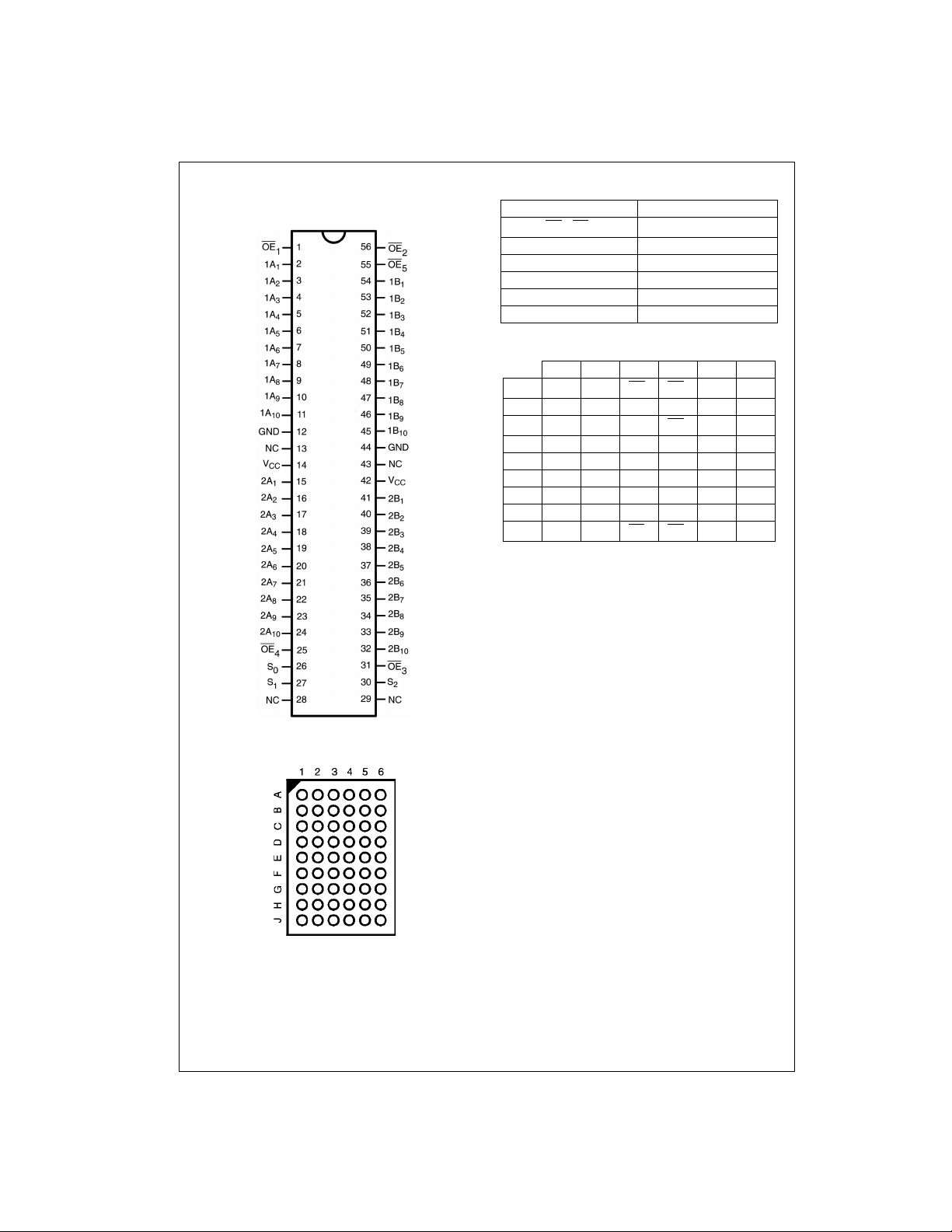
Connection Diagrams
Pin Assignment for TSSOP
FSTUD162450
Pin Descriptions
Pin Name Description
OE
, OE
1
2
Bus Switch Enables
1A, 2A Bus A
1B, 2B Bus B
S
, S
0
1
S
2
Bit Configuration Enables
Level Shifting Diode Enable
NC No Connect
FBGA Pin Assignments
123456
A 1A
B 1A51A41A11B11B41B
C 1A71A6GND OE51B61B
D 1A91A8GND V
E 2A11A
F 2A32A2S
G 2A52A4VCCGND 2B42B
H 2A72A62A102B102B62B
J 2A92A8OE4OE32B82B
1A2OE1OE21B21B
3
CC
10S0VCC1B10
S22B22B
1
1B81B
2B
3
5
7
9
1
3
5
7
9
Pin Assignment for FBGA
(Top Thru View)
www.fairchildsemi.com 2
Page 3
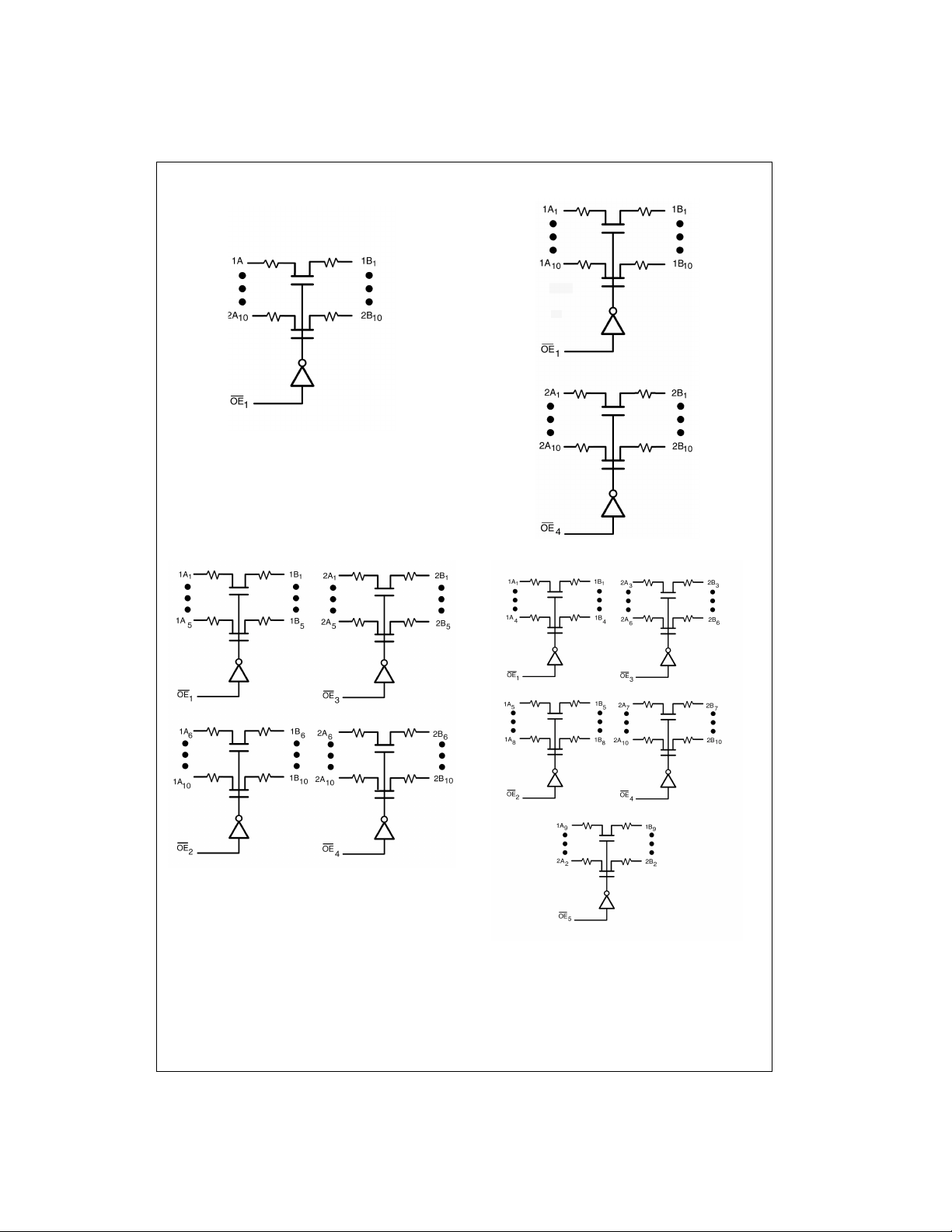
Logic Diagrams
20-Bit Configuration
FSTUD162450
10-Bit Configuration
5-Bit Configuration
4-Bit Configuration
3 www.fairchildsemi.com
Page 4
Functional Description
The device can also be configured as an 8 and 16-bit device by grounding the unused pins in the 10-bit and 20-bit configurations respectively. The 8-bit configuration may also be achieved by connecting two of the 4-bit enables from the 4-bit configuration together and connecting the remaining enable pin (OE
) HIGH.
Truth Tables
FSTUD162450
(see Functional Description)
Select Pin
S2 Mode
L Std. NMOS Switch
H Level Shifting Diode Enabled
20-Bit Configuration (S
OE
1
LXXXX 1A
OE
2
= S1 = L)
0
Inputs
OE
3
OE
OE
4
5
Inputs/Outputs
= 1B
1-10
1-10
, 2A
1-10
= 2B
1-10
HXXXX Z
10-Bit Configuration (S
= L, S1 = H)
0
Inputs Inputs/Outputs
OE
LXXLX 1A
LXXHX 1A
HXXLX Z 2A
OE
1
OE
2
OE
3
OE
4
5
1A
1-10
= 1B
= 1B
X
= 1B
X
1-10
X
X
2A
1-10
2AX = 2B
= 2B
= 2B
X
Z
HXXHX Z Z
5-Bit Configuration (S
= H, S1 = L)
0
Inputs Inputs/Outputs
OE2OE3OE4OE51A
OE
1
LLLLX1A
LLLHX1A
LLHLX1A
LLHHX1A
LHLLX1A
LHLHX1A
LHHLX1A
LHHHX1A
HLLLX Z 1A
HLLHX Z 1A
HLHLX Z 1A
HLHHX Z 1A
HHL LX Z Z 2A
HHLHX Z Z 2A
HHHLX Z Z Z 2A
1-5
, 1B
= 1B
x
= 1B
x
= 1B
x
= 1B
x
= 1B
x
= 1B
x
= 1B
x
= 1B
x
1-5
1A
, 1B
6-10
1Ay = 1B
x
1Ay = 1B
x
1Ay = 1B
x
1Ay = 1B
x
x
x
x
x
Z2A
Z2A
ZZ2A
ZZZ
= 1B
y
= 1B
y
= 1B
y
= 1B
y
6-10
y
y
y
y
y
y
y
y
2A
, 2B
1-5
2Ax = 2B
2Ax = 2B
Z2A
1-5
2A
6-10
2Ay = 2B
x
x
= 2B
y
ZZ
= 2B
x
= 2B
x
2Ax = 2B
2Ax = 2B
Z2A
2Ay = 2B
x
x
x
x
= 2B
y
2Ay = 2B
= 2B
y
ZZ
= 2B
x
= 2B
x
2Ay = 2B
x
x
= 2B
y
HHHHX Z Z Z Z
1-10
X
X
, 2B
Z
Z
Z
Z
6-10
y
y
y
y
y
y
y
y
www.fairchildsemi.com 4
Page 5

Truth Tables (Continued)
4-Bit Configuration (S
OE2OE3OE4OE51A
OE
1
LLLLL1Ax = 1B
LLLLH1Ax = 1B
LLLHL1A
LLLHH1Ax = 1B
LLHLL1A
LLHLH1Ax = 1B
LLHHL1A
LLHHH1Ax = 1B
LHLLL1A
LHLLH1Ax = 1B
LHLHL1A
LHLHH1Ax = 1B
LHHLL1A
LHHLH1Ax = 1B
LHHHL1A
LHHHH1Ax = 1B
HLLLL Z 1A
HLLLH Z 1Ay = 1B
HLLHL Z 1A
HLLHH Z 1Ay = 1B
HLHLL Z 1A
HLHLH Z 1Ay = 1B
HLHHL Z 1A
HLHHH Z 1Ay = 1B
HHL LL Z Z 2A
HHL LH Z Z 2Ax = 2B
HHLHL Z Z 2A
HHLHH Z Z 2Ax = 2B
HHHL L Z Z Z 2A
HHHLH Z Z Z 2Ay = 2B
HHHHL Z Z Z Z
HHHHH Z Z Z Z Z
= S1 = H)
0
Inputs Inputs/Outputs
1-4
, 1B
= 1B
x
= 1B
x
= 1B
x
= 1B
x
= 1B
x
= 1B
x
= 1B
x
1A
1-4
x
x
x
x
x
x
x
x
x
x
x
x
x
x
x
x
, 1B
5-8
1Ay = 1B
1Ay = 1B
1Ay = 1B
1Ay = 1B
1Ay = 1B
1Ay = 1B
1Ay = 1B
1Ay = 1B
Z2A
Z2A
Z2A
Z2A
ZZ2A
ZZ2A
ZZZ
ZZZZ
= 1B
y
= 1B
y
= 1B
y
= 1B
y
5-8
2A
, 2B
3-6
3-62A7-10
2Ax = 2B
y
y
y
y
y
y
y
y
y
y
y
y
y
y
y
y
x
2Ax = 2B
x
2Ax = 2B
x
2Ax = 2B
x
Z2A
Z2A
ZZ
ZZZ
= 2B
x
x
= 2B
x
x
= 2B
x
x
= 2B
x
x
2Ax = 2B
x
2Ax = 2B
x
2Ax = 2B
x
2Ax = 2B
x
Z2A
Z2A
ZZ
ZZZ
= 2B
x
x
x
= 2B
x
x
x
1A
7-10
y
y
9-10
2A
1Az = 1B
2Az = 2B
1A
2Az = 2B
, 2B
2Ay = 2B
2Ay = 2B
Z
ZZ
= 2B
y
= 2B
y
1Az = 1B
y
2Az = 2B
y
1A
2Az = 2B
2Ay = 2B
2Ay = 2B
Z
1Az = 1B
y
2Az = 2B
y
1A
2Az = 2B
ZZ
= 2B
y
= 2B
y
1Az = 1B
y
2Az = 2B
y
1A
2Az = 2B
2Ay = 2B
2Ay = 2B
Z
1Az = 1B
y
2Az = 2B
y
1A
2Az = 2B
ZZ
= 2B
y
= 2B
y
1Az = 1B
y
2Az = 2B
y
1A
2Az = 2B
2Ay = 2B
2Ay = 2B
Z
1Az = 1B
y
2Az = 2B
y
1A
2Az = 2B
ZZ
= 2B
y
1Az = 1B
y
2Az = 2B
y
1A
2Az = 2B
1-2
, 1B
, 2B
Z
= 1B
z
Z
= 1B
z
Z
= 1B
z
Z
= 1B
z
Z
= 1B
z
Z
= 1B
z
Z
= 1B
z
Z
= 1B
z
9-10
1-2
z
z
z
z
z
z
z
z
z
z
z
z
z
z
z
z
z
z
z
z
z
z
z
z
z
z
z
z
z
z
z
z
FSTUD162450
5 www.fairchildsemi.com
Page 6

Absolute Maximum Ratings(Note 2) Recommended Operating
Supply Voltage (VCC) −0.5V to +7.0V
DC Switch Voltage (V
) (Note 3) −2.0V to +7.0V
S
DC Input Control Pin Voltage
(V
) (Note 4) −0.5V to +7.0V
FSTUD162450
IN
DC Input Diode Current (l
DC Output (I
DC V
CC
) Current 128 mA
OUT
/GND Current (ICC/I
) VIN < 0V −50 mA
IK
GND
Storage Temperature Range (T
) +/− 100 mA
) −65°C to +150 °C
STG
Conditions
Power Supply Operating (V
Input Voltage (V
Output Voltage (V
Free Air Operating Temperature (T
Note 2: The “Absolute Maximum Ratings” are those values bey ond which
the safety of the d evice cannot be guaranteed. The device sh ould not be
operated at these limit s. The parametric values defin ed in the Electrical
Characteristics tables are not guaranteed at the absolute maximum rating.
The “Recomme nded O peratin g Cond itions ” table will defin e the condition s
for actual device operation.
is the voltage observed/applied at either the A or B Ports across
Note 3: V
S
the switch.
Note 4: The input and output ne gative vo ltage ra tings may be excee ded if
the input and output diode current ratings are observed.
Note 5: Unused control inputs must be held HIGH or LOW. They may not
float.
(Note 5)
CC)
)0V to 5.5V
IN
)0V to 5.5V
OUT
)-40 °C to +85 °C
A
DC Electrical Characteristics
Symbol Parameter
V
V
V
V
I
I
I
OZ
R
Clamp Diode Voltage 4.5 −1.2 V IIN = −18 mA
IK
HIGH Level Input Voltage 4.0-5.5 2.0 V IF S2 = HIGH 4.5V ≤ VCC ≤ 5.5V
IH
LOW Level Input Voltage 4.0-5.5 0.8 V IF S2 = HIGH 4.5V ≤ VCC ≤ 5.5V
IL
HIGH Level Output Voltage 4.5-5.5 see Figure 4 V S2 = V
OH
Input Leakage Current 5.5 ±1.0 µA0 ≤ VIN ≤ 5.5V
OFF-STATE Leakage Current 5.5 ±1.0 µA0 ≤ A, B ≤ V
Switch On Resistance 4.5 20 26 38 Ω VIN = 0V, IIN = 64 mA, S2 = 0V or V
ON
(V) Min Typ
(Note 7) 4.5 20 27 40 Ω VIN = 0V, IIN = 30 mA, S2 = 0V or V
4.5 20 28 48 Ω VIN = 2.4V, IIN = 15 mA, S2 = 0V
4.0 20 30 48 Ω V
4.5 20 35 50 Ω V
V
I
CC
Quiescent Supply Current
5.5
∆ I
Increase in I
CC
CC
per Input
5.5
V
Voltage Undershoot 5.5 −2.0 V 0.0 mA ≥ IIN ≥ −50 mA
IKU
Note 6: Typi c al values are at VCC = 5.0V and TA = +25°C
Note 7: Measured by the volta ge drop between A an d B pins at the indicated c urrent through the switch. On Resistance is determined by the lower of the
voltages on the two (A or B) pins.
TA = −40 °C to +85 °C
CC
(Note 6)
010µAV
Units Conditions
Max
IN
IN
IN
3 µAS2 = GND, VIN = VCC or GND, I
10 µAS2 = VCC, OEX = VCC, VIN = VCC or GND, I
1.5 mA S2 = VCC, OEX = GND, VIN = VCC or GND, I
2.5 mA
4.0 mA
One Input at 3.4V
Other Inputs at VCC or GND, S2 = 0V
One Input at 3.4V
Other Inputs at VCC or GND, S2 = V
OEx = 5.5V
CC
= 5.5V
CC
= 2.4V, IIN = 15 mA, S2 = 0V
= 2.4V, IIN = 15 mA, S2 = V
CC
OUT
4.0V to 5.5V
CC
CC
= 0
OUT
OUT
CC
= 0
= 0
www.fairchildsemi.com 6
Page 7

AC Electrical Characteristics
= −40 °C to +85 °C,
T
A
C
Symbol Parameter
= 50pF, RU = RD = 500Ω
L
= 4.5 – 5.5V VCC = 4.0V (S2 = 0V)
V
CC
Units
Conditions Figure
Number
Min Max Min Max
t
, t
PHL
t
PZH
t
PHZ
t
PZH
t
PHZ
Note 8: This par ameter is guaranteed by desi gn but is not test ed. The bus switch contribut es no propagati on delay other than the RC dela y of the typical On
Resistance of the sw it c h and the 50pF load capa citance, when drive n by an ideal voltage sourc e (zero output impe dance).
Propagation Delay Bus-to-Bus
PLH
(Note 8)
, t
Output Enable Time 1.5 7.5 8.0 ns VI = 7V for t
PZL
, t
Output Disable Time 1.5 7.7 8.2 ns VI = 7V for t
PLZ
, t
, t
PZLSel
PLZSel
(S
) to Output Enable Time 1.5 8.0 8.5 ns VI = 7V for t
0, 1
(S
) to Output Disable Time 1.5 8.5 8.7 ns VI = 7V for t
0, 1
1.25 1.25 ns VI = OPEN Figures
VI = OPEN for t
PZL
VI = OPEN for t
PLZ
= OPEN for t
I
= OPEN for t
I
PZL
PLZ
V
V
PZH
PHZ
PZH
PHZ
Figures
Figures
Figures
Figures
AC Electrical Characteristics: Translating Diode
T
= −40 °C to +85 °C,
A
= 50pF, RU = RD = 500Ω
C
Symbol Parameter
L
VCC = 4.5 – 5.5V (S2 = VCC)
Units
Min Max
t
, t
PHL
t
PZH
Propagation Delay Bus-to-Bus (Note 9) 1.25 ns VI = OPEN Figures
PLH
, t
Output Enable Time 1.5 10.0 ns VI = 7V for t
PZL
VI = OPEN for t
t
, t
PHZ
Output Disable Time 1.5 9.0 ns VI = 7V for t
PLZ
VI = OPEN for t
t
PZH
, t
PZLSel
(S
) to Output Enable Time 1.5 11.0 ns VI = 7V for t
0, 1
VI = OPEN for t
t
PHZ
, t
PLZSel
(S
) to Output Disable Time 1.5 10.0 ns VI = 7V for t
0, 1
V
Note 9: This parameter is guaranteed by design but is not tested. This bus switch contributes no propagation delay other than the RC delay of the typical On
Resistance of the sw it c h and the 50pF load capa citance, when drive n by an ideal voltage sourc e (zero output impe dance).
Conditions Figure
PZL
PZH
PLZ
PHZ
PZL
PZH
PLZ
= OPEN for t
I
PHZ
Number
Figures
Figures
Figures
Figures
FSTUD162450
2, 3
2, 3
2, 3
2, 3
2, 3
2, 3
2, 3
2, 3
2, 3
2, 3
Capacitance (Note 10)
Symbol Parameter Typ Max Units Conditions
C
IN
C
I/O
Note 10: TA = +25°C, f = 1 MHz, Capacitance is characterized but not tested.
Control Pin Input Capacitance 3.5 pF VCC = 5.0V, VIN = 0V
Input/Output Capacitance “OFF State” 6pFV
, OE = 5.0V, VIN = 0V
CC
7 www.fairchildsemi.com
Page 8

Undershoot Characteristic (Note 11)
Symbol Parameter Min Typ Max Units Conditions
V
OUTU
Note 11: This test is intended to characterize the device’s protective capabilities by maintaining output signal integrity during an input transient volt age
undershoot event.
Output Voltage During Undershoot 2.5 VOH − 0.3 V Figure 1
FSTUD162450
FIGURE 1.
Device Test Conditions Transie nt
Parameter Value Units
V
IN
R1 = R
V
TRI
V
CC
2
see Waveform V
100K Ω
11.0 V
5.5 V
Input Voltage (V
) Waveform
IN
AC Loading and Waveforms
FIGURE 2. AC Test Circuit
FIGURE 3. AC Waveforms
www.fairchildsemi.com 8
Note: Input driven by 50Ω source terminated in 50Ω
includes load and stray capacitance
Note: C
L
Note: Input Frequency = 1.0 MHz, t
= 500 ns
W
Page 9

FSTUD162450
FIGURE 4.
9 www.fairchildsemi.com
Page 10

Physical Dimensions inches (millimeters) unless otherwise noted
FSTUD162450
54-Ball Fine-Pitch Ball Grid Array (FBGA), JEDEC MO-205, 5.5mm Wide
www.fairchildsemi.com 10
Package Number BGA54A
Preliminary
Page 11

Physical Dimensions inches (millimeters) unless otherwise noted (Continued)
Physical Dimensions inches (millimeters) unless otherwise noted (Continued)
FSTUD162450 Configurable 4-Bit to 20-Bit Bus Switch with
Shifting and 25
Ω
Series Resistors in Outputs
56-Lead Thin Shrin k Small Ou tlin e Pack age (TSSOP), JEDEC MO-153, 6.1mm Wide
Package Number MTD56
Technology Description
The Fairchild Switch family derives from and embodies Fairchild’s proven switch t echnology used for several years in it s
74LVX3L384 (FST3384) bus switch product.
Fairchild does not assume any responsibility for use of any circuitry described , no circuit patent licenses are implied and
Fairchild reserves the right at any time without notice to change said circuitry and specifications.
LIFE SUPPORT POLICY
FAIRCHILD’S PRODUCTS ARE NOT AUTHORIZED FOR USE AS CRITICAL COMPONENTS IN LIFE SUPPORT
DEVICES OR SYSTEMS WITHOUT THE EXPRESS WRITTEN APPROVAL OF THE PRESIDENT OF FAIRCHILD
SEMICONDUCTOR CORPORATION. As used herein:
1. Life support devices or systems are dev ic es or syste ms
which, (a) are intended for surgical implant into the
body, or (b) support or sustain life, and (c) whose failure
to perform when properly used in accordance with
instructions for use provide d in the l abe ling, can be reasonably expected to result in a significant injury to the
user.
2. A critical compo nent in any com ponen t of a life s upp ort
device or system whose failure to perform can be reasonably expected to cause the failure of the life support
device or system, or to affect its safety or effectiveness.
www.fairchildsemi.com
11 www.fairchildsemi.com
−
2V Undershoot Protection and Selectable Level
 Loading...