

Page 1
March 2008
FSUSB22 — Low-Power, 2-Port, High-Speed USB 2.0
FSUSB22 — Low-Power, 2-Port, High-Speed USB 2.0 (480Mbps) Switch
(480Mbps) Switch
Features
-40dB Off Isolation at 250MHz
-40dB Non-adjacent Channel Crosstalk at 250MHz
On Resistance: 4.5Ω Typical (RON)
-3dB Bandwidth: 750MHz
Low-Power Consumption: 1µA Maximum
Control Input: TTL Compatible
Bi-directional Operation
USB High-Speed and Full-Speed Signaling
Capability
Applications
Cell Phones, PDAs, Digital Cameras, Notebook
Computers
Ordering Information
Operating
Part Number
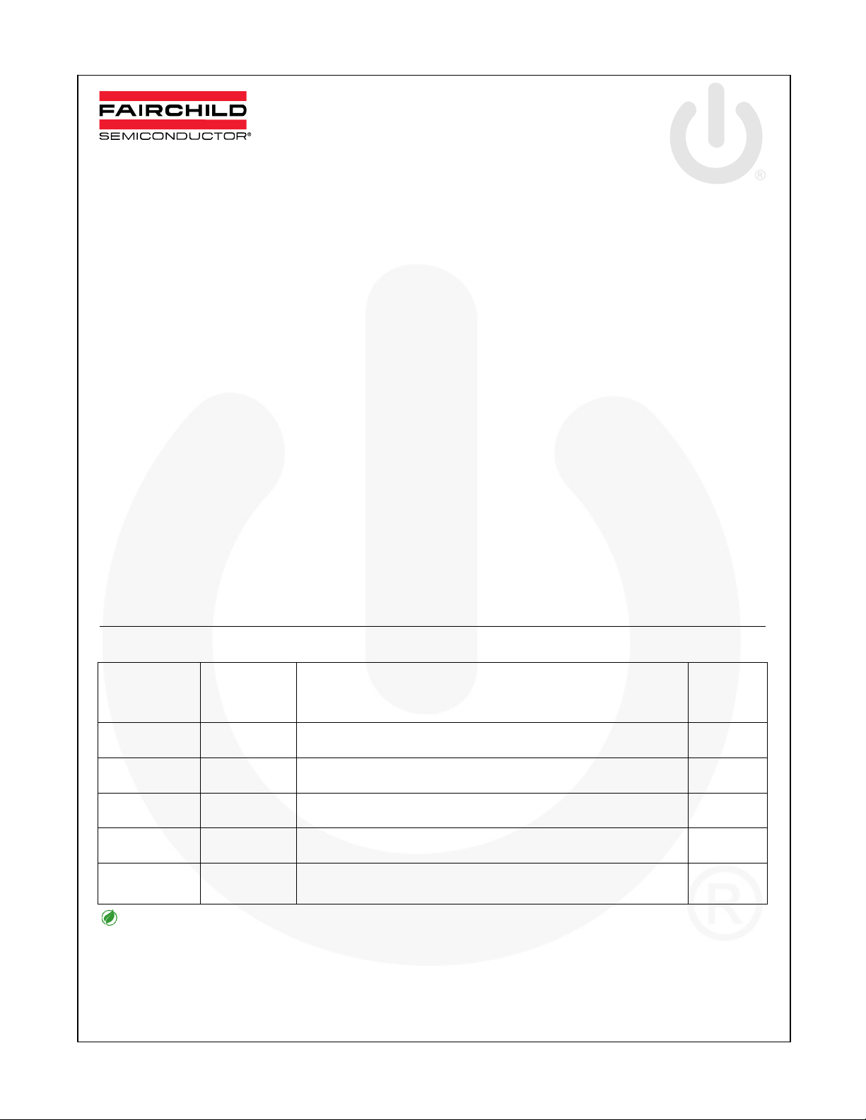
FSUSB22BQX
FSUSB22QSC
FSUSB22QSCX
FSUSB22MTC
FSUSB22MTCX
All packages are lead free per JEDEC: J-STD-020B standard.
Temperature
Range
-40 to +85°C
-40 to +85°C
-40 to +85°C
-40 to +85°C
-40 to +85°C
16-Terminal Depopulated Quad Very-Thin Flat Pack No Leads
(DQFN), JEDEC MO-241, 2.5 x 3.5mm
16-Lead Quarter Size Outline Package (QSOP), JEDEC MO-137,
0.150-inch Wide
16-Lead Quarter Size Outline Package (QSOP), JEDEC MO-137,
0.150-inch Wide
16-Lead Thin Shrink Small Outline Package (TSSOP), JEDEC
MO-153, 4.4mm Wide
16-Lead Thin Shrink Small Outline Package (TSSOP), JEDEC
MO-153, 4.4mm Wide
Description
FSUSB22 is a low-power, high-bandwidth switch
specially designed for applications switching high-speed
USB 2.0 signals in handset and consumer applications;
such as cell phone, digital camera, and notebook with
hubs or controllers of limited USB I/O. The wide
bandwidth (750MHz) allows signals to pass with
minimum edge and phase distortion. Superior channelto-channel crosstalk results in minimal interference. It is
compatible with the USB2.0 Hi-Speed standard.
.
Package
Packing
Method
Tape and
Reel
Tube
Tape and
Reel
Tube
Tape and
Reel
©2005Fairchild Semiconductor Corporation www.fairchildsemi.com
FSUSB22 • Rev. 1.0.3
Page 2
Logic Diagram Analog Symbol
D-
USB
Port
Docking Station
Docking Connector
D+
1B
2
1B
1A
1
3
2
4
D+
USB
D-
Port
FSUSB22 — Low-Power, 2-Port, High-Speed USB 2.0 (480Mbps) Switch
V
S
CC
16
1
15
/OE
4B
14
1
4B
13
2
USB 2.0
Host
Controller
D+
D-
D+
D-
FSUSB22
Notebook Computer
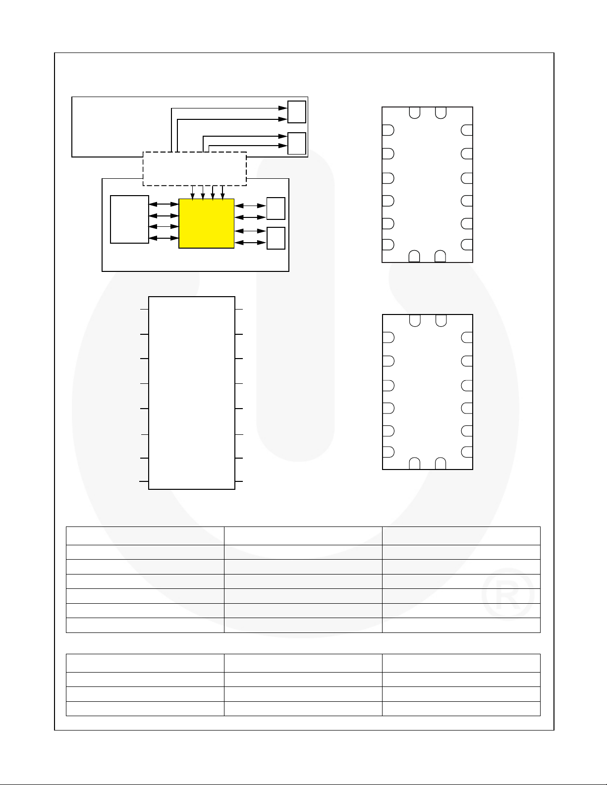
Figure 1. Logic Diagram
1
S
2
1B
1
3
1B
2
4
1A
5
2B
1
6
2B
2
7
2A
GND
8
D+
USB
Port
D-
D+
USB
D-
Port
V
16
CC
/OE
15
4B
14
1
4B
13
2
4A
12
3B
11
1
3B
10
2
3A
9
2B
2B
2A
5
1
6
2
7
8
12
11
10
9
GND 3A
Figure 2. Analog Symbol
V
S
CC
116
1B
1B
2B
2B
1A
2A
2
1
3
2
4
5
1
6
2
7
8
GND 3A
15
14
13
12
11
10
9
4A
3B
3B
/OE
4B
4B
4A
3B
3B
1
2
1
2
1
2
Figure 3. QSOP and TSSOP Pin Configuration Figure 4. Pad Assignment for DQFN
Pin Descriptions
Pin # Pin Names Description
1 S Select Input
2,3,5,6,10,11,13,14 1B1,1B2, 2B1,2B2,3B2,3B1,4B2,4B1 Bus B
8 GND Ground
4,7,9,12 1A,2A,3A,4A Bus A
15 /OE Bus Switch Enable
16 VCC Supply Voltage
Truth Table
S OE Function
Don’t Care HIGH Disconnect
LOW LOW A=B1
HIGH LOW A=B2
© 2005 Fairchild Semiconductor Corporation www.fairchildsemi.com
FSUSB22 • Rev. 1.0.3 2
Page 3
FSUSB22 — Low-Power, 2-Port, High-Speed USB 2.0 (480Mbps) Switch
Absolute Maximum Ratings
Stresses exceeding the absolute maximum ratings may damage the device. The device may not function or be
operable above the recommended operating conditions and stressing the parts to these levels is not recommended.
In addition, extended exposure to stresses above the recommended operating conditions may affect device
reliability. The absolute maximum ratings are stress ratings only.
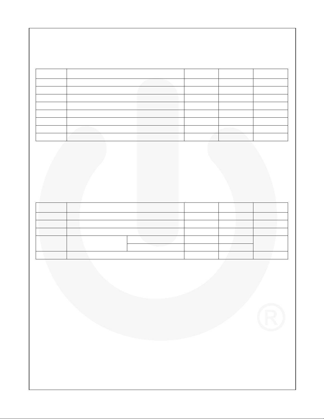
Symbol Parameter Min. Max. Unit
VCC Supply Voltage -0.5 4.6 V
VS DC Switch Voltage -0.5 VCC + 0.05 V
VIN DC Input Voltage
IIK DC Input Diode Current, VIN<0V -50 mA
I
DC Output Sink Current 128 mA
OUT
I
/ I
CC
DC V
GND
T
Storage Temperature Range -65 +150 °C
STG
/ GND Current ±100 mA
CC
ESD Human Body Model, JESD22-A114 4 kV
Note:
1. The input and output negative voltage ratings may be exceeded if the input and output diode current ratings are
observed.
(1)
-0.5 4.6 V
Recommended Operating Conditions
The Recommended Operating Conditions table defines the conditions for actual device operation. Recommended
operating conditions are specified to ensure optimal performance to the datasheet specifications. Fairchild does not
recommend exceeding them or designing to Absolute Maximum Ratings.
Symbol Parameter Min. Max. Unit
VCC Power Supply Operating 3.0 3.6 V
VIN Input Voltage 0 VCC V
V
Output Voltage 0 VCC V
OUT
tr, tf Input Rise and Fall Time
Switch Control Input
Switch I/O 0 DC
TA Operating Temperature, Free Air -40 +85 °C
Note:
2. Unused control inputs must be held HIGH or LOW. They may not float.
(2)
0 5
ns/V
© 2005 Fairchild Semiconductor Corporation www.fairchildsemi.com
FSUSB22 • Rev. 1.0.3 3
Page 4
DC Electrical Characteristics
Typical values are at V
= 3.0V and TA = 25°C.
CC
FSUSB22 — Low-Power, 2-Port, High-Speed USB 2.0 (480Mbps) Switch
Symbol Parameter Conditions VCC (V)
TA=-40 to +85°C
Min. Typ. Max.
VIK Clamp Diode Voltage I
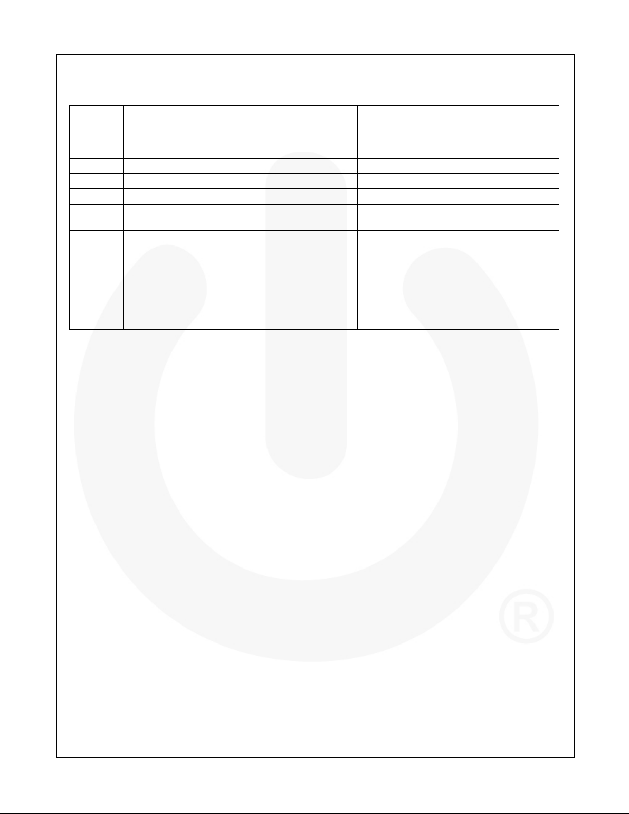
VIH High-Level Input Voltage 3.0 to 3.6 2.0 V
VIL Low-Level Input Voltage 3.0 to 3.6 0.8 V
IIN Input Leakage Current
I
OFF
RON Switch On Resistance
ΔRON
R
FLAT(ON)
Off-state Leakage
Current
Delta R
ON
On Resistance Flatness
(3)
ICC Quiescent Supply Current
Notes:
3. Measured by the voltage drop between the A and B pins at the indicated current through the switch. On
resistance is determined by the lower of the voltages on the A or B pins.
4. Flatness is defines as the difference between the maximum and the minimum value on resistance over the
specified range of conditions.
= -18mA 3.0 -1.2 V
IN
0 ≤ VIN ≤ 3.6V
0 ≤ A, B ≤ VCC
3.6 ±1.0 µA
3.6 ±1.0 µA
VIN = 0.8V, ION = 8mA 3.0 5 7
V
= 3.0V, ION = 8mA 3.0 4.5 6.5
IN
VIN = 0.8V, VIN = 0V - 1.5,
I
= 8mA
ON
(4)
I
= 8mA 3.0 1
OUT
VIN = VCC or GND,
I
= 0
OUT
3.0 0.3
3.6 1 µA
Units
Ω
Ω
Ω
© 2005 Fairchild Semiconductor Corporation www.fairchildsemi.com
FSUSB22 • Rev. 1.0.3 4
Page 5
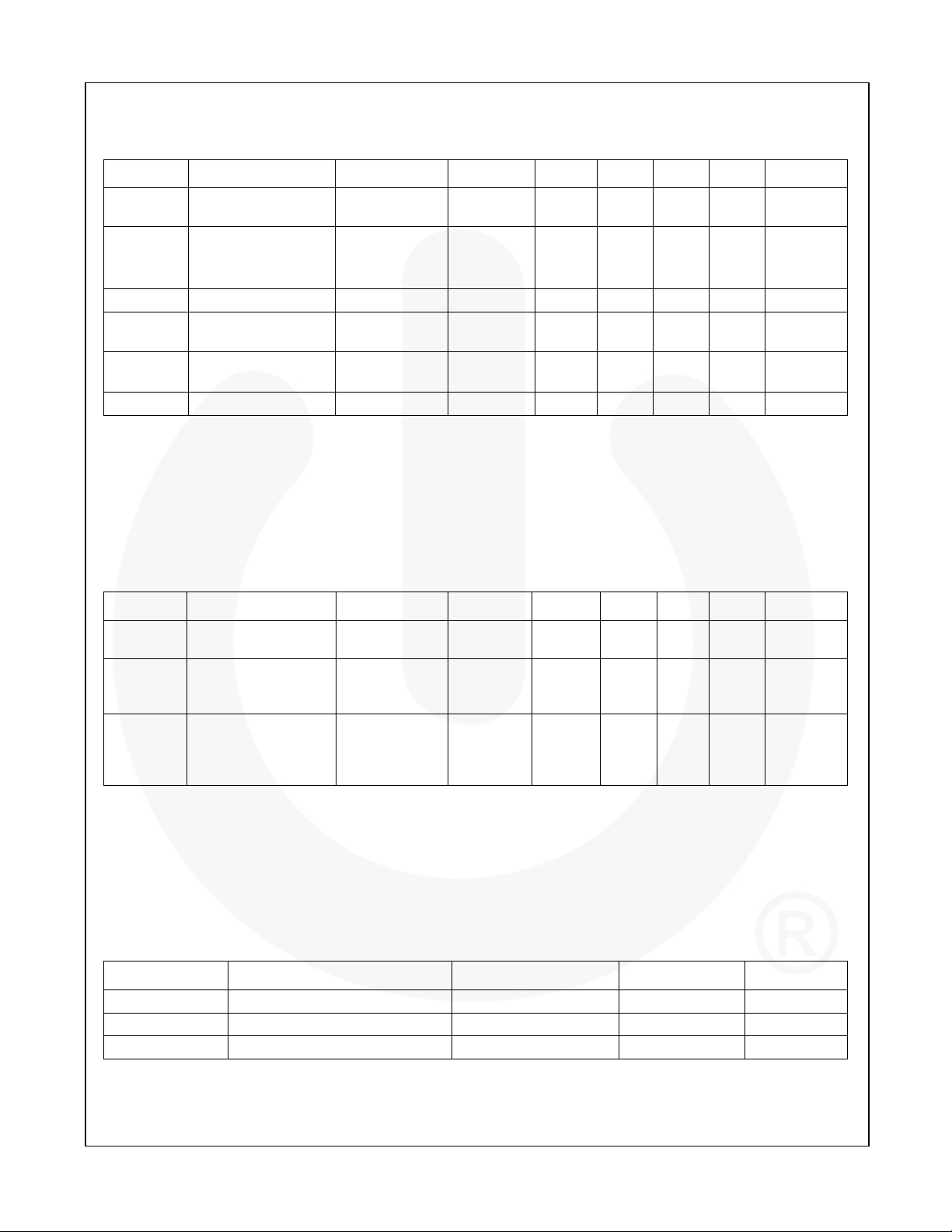
AC Electrical Characteristics
Typical values are at V
Symbol Parameter Conditions VCC(V) Min. Typ. Max. Units Figure
tON
Turn-on Time
S-to-Bus B
= 3.0V and TA = 25°C.
CC
3.0 to 3.6 4.5 6.0 ns
Figure 9
Figure 10
FSUSB22 — Low-Power, 2-Port, High-Speed USB 2.0 (480Mbps) Switch
t
OFF
Turn-off Time
S-to-Bus B
3.0 to 3.6 2.5 4.0 ns
Figure 9
Figure 10
tPD Propagation Delay CL = 10pF 3.0 to 3.6 0.25 ns Figure 14
Non-Adjacent Off
Isolation
Non-Adjacent
Channel Crosstalk
X
O
IRR
TALK
BW -3dB Bandwidth
f = 250MHz,
R
= 50Ω
L
f = 250MHz,
R
= 50Ω
L
RL = 50Ω
3.0 to 3.6 -30 dB Figure 11
3.0 to 3.6 -38 dB Figure 12
3.0 to 3.6 750 MHz Figure 13
USB Related AC Electrical Characteristics
Typical values are at V
Symbol Parameter Conditions VCC (V) Min. Typ. Max. Units Figure
t
SK(O)
t
SK(P)
TJ Total Jitter
Channel-to Channels
Skew
Skew of Opposite
Transition of the
Same Output
= 3.0V and TA = 25°C.
CC
CL = 10pF 3.0 to 3.6 0.051 pF
CL = 10pF 3.0 to 3.6 0.020 pF
= 50Ω,
R
L
C
= 10pF
L
t
= tF = 750ps
R
at 480MPs
Figure 14
Figure 16
Figure 14
Figure 16
3.0 to 3.6 0.210
Capacitance
Typical values are at V
Symbol Parameter Conditions Typ. Unists
CIN Control Pin Input Capacitance VCC = 0V 2.5 pF
CON A/B On Capacitance VCC = 3.3V, /OE = 0V 12 pF
C
Port B Off Capacitance VCC and /OE = 3.3V 4.5 pF
OFF
= 3.0V and TA = 25°C.
CC
© 2005 Fairchild Semiconductor Corporation www.fairchildsemi.com
FSUSB22 • Rev. 1.0.3 5
Page 6
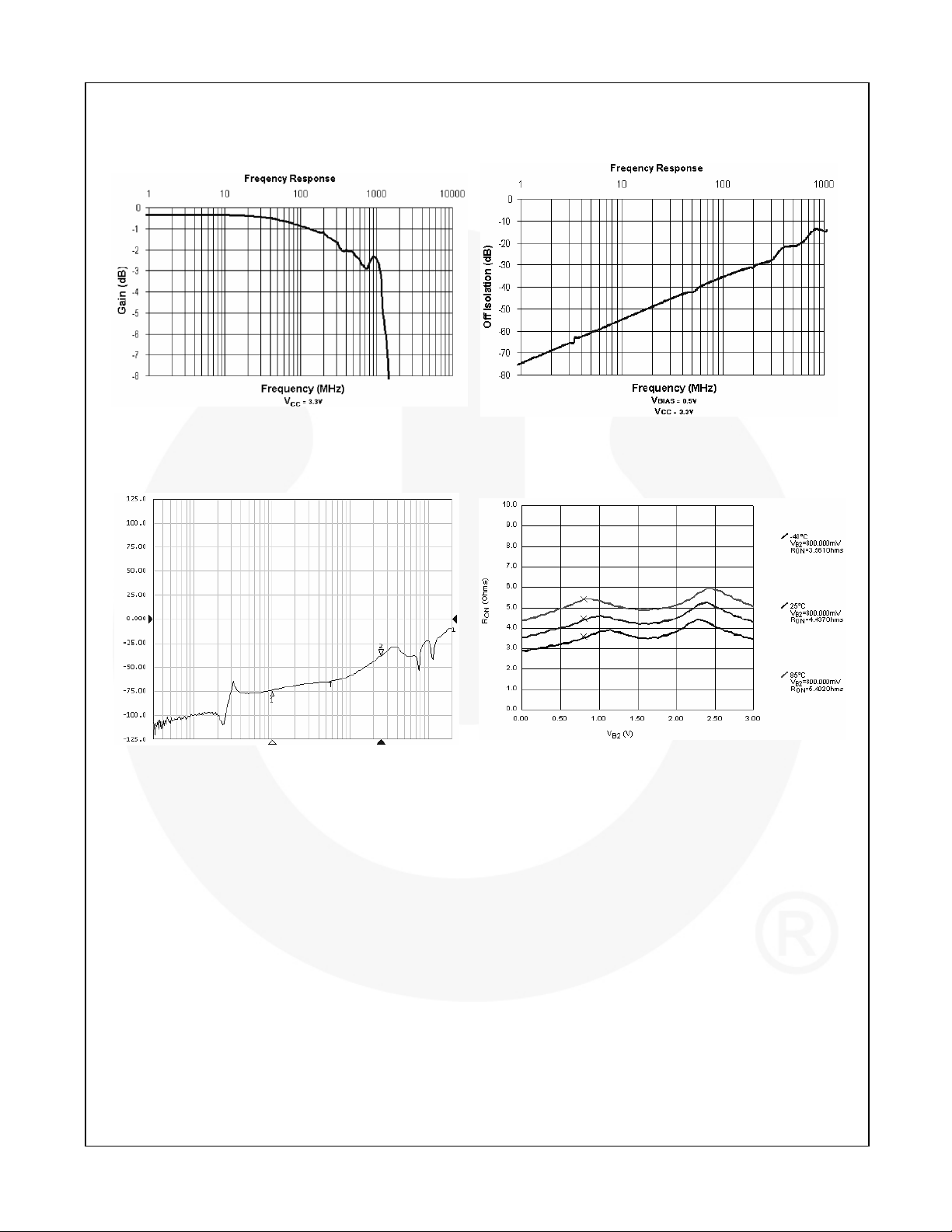
Performance Characteristics
FSUSB22 — Low-Power, 2-Port, High-Speed USB 2.0 (480Mbps) Switch
Figure 5. Gain vs. Frequency Figure 6. Off Isolation
Figure 7. Crosstalk Figure 8. RON
© 2005 Fairchild Semiconductor Corporation www.fairchildsemi.com
FSUSB22 • Rev. 1.0.3 6
Page 7
/
5
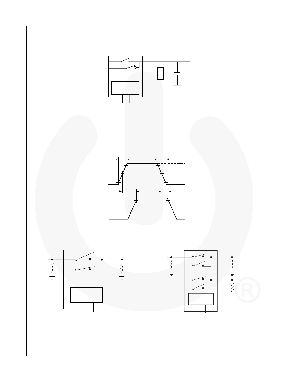
AC Loadings and Waveforms
FSUSB22 — Low-Power, 2-Port, High-Speed USB 2.0 (480Mbps) Switch
B
1
B
2
Control
OE
S
Notes: Input driven by 50Ω source terminated in 50Ω.
CL includes load and stray capacitance.
Input PRR-1.0MHz, tW = 500ns.
Figure 9. AC Test Circuit
tr = 2.5ns tf = 2.5ns
SELECT
INPUT
10% 10%
t
ON
OUTPUT
90%
1.5V
A
50Ω
GND
90%
1.5V
t
90% 90%
OFF
10pF
3.0V
GND
V
OH
V
OL
Figure 10. AC Waveforms
B
1
50Ω
B
2
S
Figure 11. Off Isolation Test Figure 12. Crosstalk Test
© 2005 Fairchild Semiconductor Corporation www.fairchildsemi.com
FSUSB22 • Rev. 1.0.3 7
Control
/OE
A
50Ω
B
100Ω
0
50Ω
A
100Ω
1
S
Control
/OE
Page 8
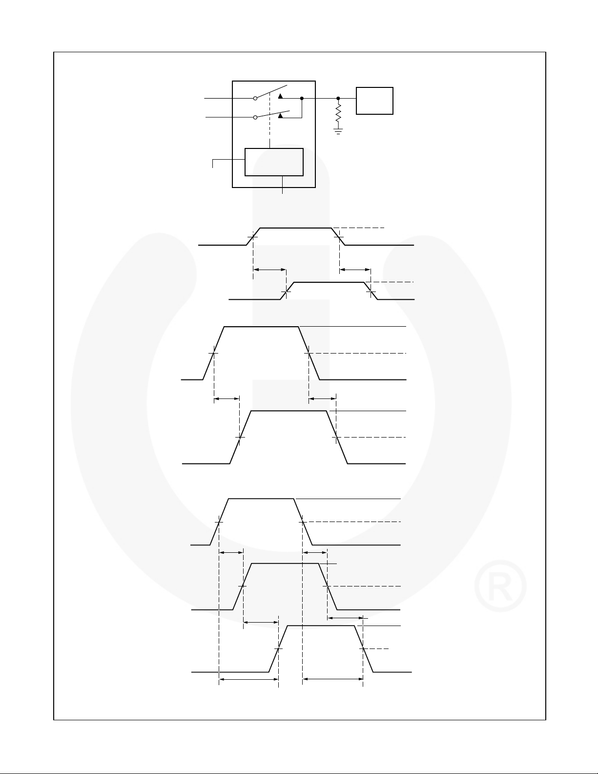
AC Loadings and Waveforms
FSUSB22 — Low-Power, 2-Port, High-Speed USB 2.0 (480Mbps) Switch
Input
400mV
Input
GND
Output
t
PLH
B
S
Control
/OE
Figure 13. Bandwidth Test
50% 50%
t
PLH
50% 50%
Figure 14. Propagation Delay
50Ω
A
Monitor
800mV
t
PHL
V
OH
V
OL
800mV
50%50%
400mV
0
t
PHL
V
OH
50%
50%
Output
V
t
= | t
- t
PLH2
PHL
| or | t
|
SP(P)
t
PHL1
PHL1
- t
PHL2
SK(O)
0
t
SK(O)
t
PHL2
|
SK(P)
PHL
Figure 15. Pulse Skew t
Input
t
PLH1
50% 50%
Output 1
t
SK(O)
Output 2
t
PLH2
t
= | t
PLH1
- t
SK(O)
Figure 16. Output Skew t
© 2005 Fairchild Semiconductor Corporation www.fairchildsemi.com
FSUSB22 • Rev. 1.0.3 8
OL
800mV
50%50%
400mV
50%50%
Page 9
Physical Dimensions
FSUSB22 — Low-Power, 2-Port, High-Speed USB 2.0 (480Mbps) Switch
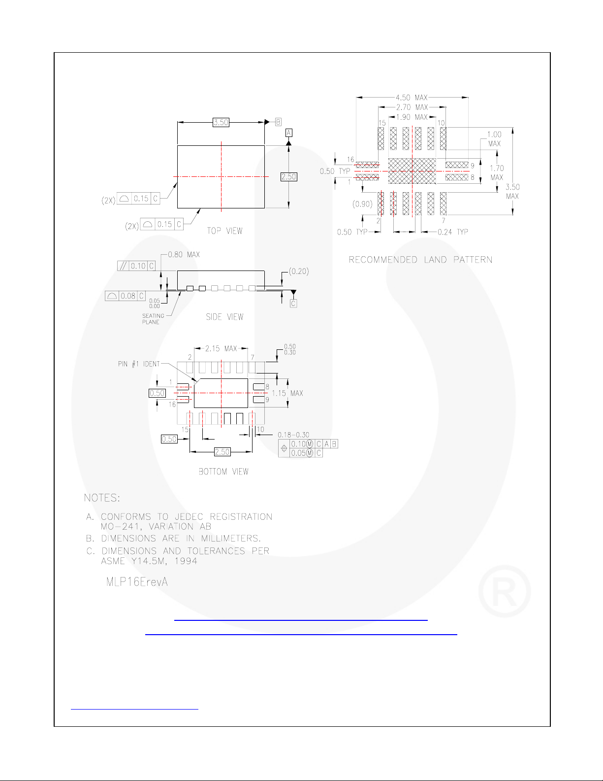
Figure 17. 16-Terminal Depopulated Quad Very-Thin Flat Pack No Leads (DQFN), JEDEC MO-241,2.5 x 3.5mm
Note: click here for tape and reel specifcations, available at:
http://www.fairchildsemi.com/products/analog/pdf/MLP16_25x35_TNR.pdf
Package drawings are provided as a service to customers considering Fairchild components. Drawings may change in any manner
without notice. Pl ease note the revision and/or date on t he drawing and contact a Fairchild S emiconductor representative to v er ify
or obtain the most recent revision. Package specifications do not expand the terms of Fairchild’s worldwide terms and conditions, specifically
the warranty therein, which covers Fairchild products.
Always visit Fairchild Semiconductor’s online packaging area for the most recent package drawings:
http://www.fairchildsem i.com/p ackagi ng/
© 2005 Fairchild Semiconductor Corporation www.fairchildsemi.com
FSUSB22 • Rev. 1.0.3 9
Page 10
Physical Dimensions
TOP VIEW
FSUSB22 — Low-Power, 2-Port, High-Speed USB 2.0 (480Mbps) Switch
LAND PATTERN
RECOMMENDATION
SIDE VIEW
END VIEW
DETAIL A
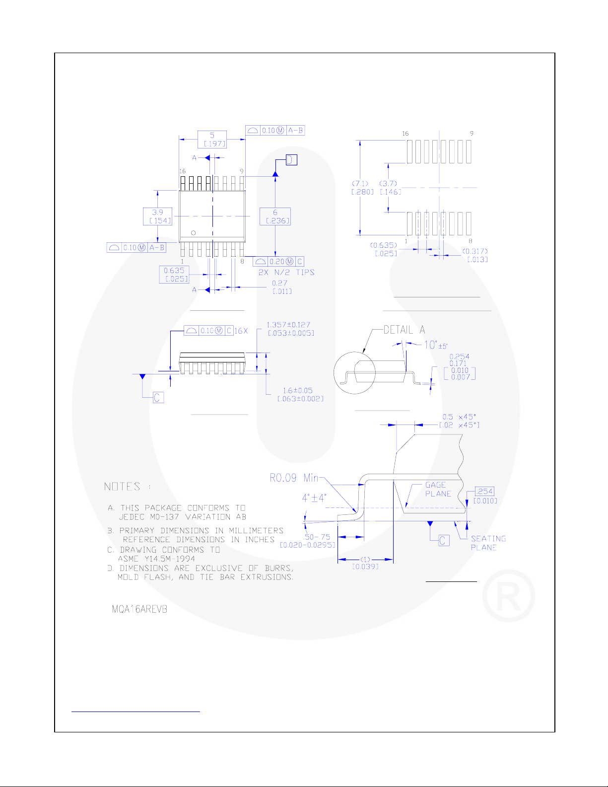
Figure 18. 16-Lead Quarter Size Outline Package (QSOP), JEDEC MO-137, 0.150-inch Wide
Package drawings are provided as a service to customers considering Fairchild components. Drawings may change in any manner
without notice. Pl ease note the revision and/or date on t he drawing and contact a Fairchild S emiconductor representative to v er ify
or obtain the most recent revision. Package specifications do not expand the terms of Fairchild’s worldwide terms and conditions, specifically
the warranty therein, which covers Fairchild products.
Always visit Fairchild Semiconductor’s online packaging area for the most recent package drawings:
http://www.fairchildsem i.com/p ackagi ng/
© 2005 Fairchild Semiconductor Corporation www.fairchildsemi.com
FSUSB22 • Rev. 1.0.3 10
Page 11
Physical Dimensions
5.00±0.10
FSUSB22 — Low-Power, 2-Port, High-Speed USB 2.0 (480Mbps) Switch
4.55
5.90
7.354.45
0.11
4.4±0.1
0.65
1.45
5.00
12°
MTC16rev4
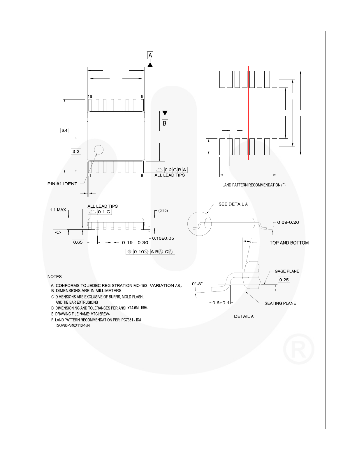
Figure 19. 16-Lead Thin Shrink Small Outline Package (TSSOP), JEDEC MO-153, 4.4mm Wide
Package drawings are provided as a service to cust omers considering Fairchild components. Drawings may change in any manner
without notice. Pl ease note the revision and/or date on t he drawing and contact a Fairchild S emiconductor representative to v er ify
or obtain the most recent revision. Package specifications do not expand the terms of Fairchild’s worldwide terms and conditions, specifically
the warranty therein, which covers Fairchild products.
Always visit Fairchild Semiconductor’s online packaging area for the most recent package drawings:
http://www.fairchildsem i.com/p ackagi ng/
© 2005 Fairchild Semiconductor Corporation www.fairchildsemi.com
FSUSB22 • Rev. 1.0.3 11
Page 12
FSUSB22 — Low-Power, 2-Port, High-Speed USB 2.0 (480Mbps) Switch
© 2005 Fairchild Semiconductor Corporation www.fairchildsemi.com
FSUSB22 • Rev. 1.0.3 12
 Loading...