

Page 1
May 2012
FSTD3125 — 4-Bit Bus Switch with Level Shifting
FSTD3125 — 4-Bit Bus Switch with Level Shifting
Features
4Ω Switch Connection between Two Ports
Minimal Propagation Delay through the Switch
Low I
CC
Zero Bounce in Flow-through Mode
Control Inputs Compatible with TTL Level
TruTranslation Voltage Translation from 5.0V Inputs
to 3.3V Outputs
Ordering Information
Operating
Part Number
FSTD3125MTCX -40 to 85°C
Temperature
Range
14-Lead, Thin Shrink Small Outline Package (TSSOP), JEDEC
MO-153, 4mm Wide
Description
Fairchild switch FSTD3125 provides four high-speed
CMOS TTL-compatible bus switches. The low on
resistance of the switch allows inputs to be connected to
outputs without adding propagation delay or generating
additional ground bounce noise. A diode to V
been integrated into the circuit to allow for level shifting
between 5V inputs and 3.3V outputs.
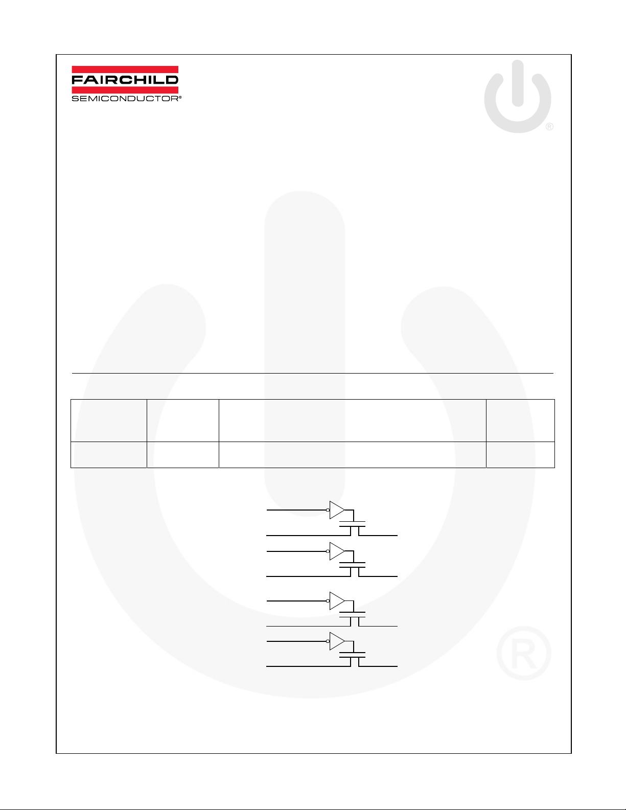
The device is organized as four one-bit switches with
separate /OE inputs. When /OE is LOW, the switch is
ON and port A is connected to port B. When /OE is
HIGH, the switch is OPEN and a high-impedance state
exists between the two ports.
Package
Packing
Tape and Reel
has
CC
Method
1
/OE
1
23
1A
4
/OE
2
56
2A
10
/OE
3
9
3A
13
/OE
4
4A
1B
2B
8
3B
1112
4B
Figure 1. Logic Diagram
© 2001 Fairchild Semiconductor Corporation www.fairchildsemi.com
FSTD3125 • Rev. 1.0.3
Page 2
4
3
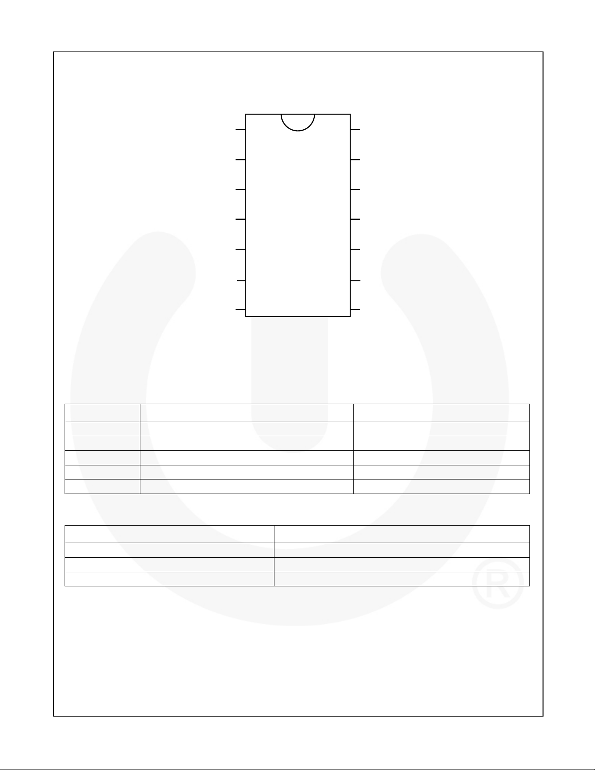
Pin Configuration
FSTD3125 — 4-Bit Bus Switch with Level Shifting
Pin Descriptions
1A
1B
2A
2B
1
1
2
3
4
2
5
6
7
/OE
/OE
GND
Figure 2. Pin Assignments
14
13
12
11
10
V
CC
/OE
4A
4B
/OE
3A
9
3B
8
Pin # Pin Names Description
1, 4, 10, 13 /OE1, /OE2, /OE3, /OE4 Bus Switch Enables
2, 5, 9, 12 1A, 2A, 3A, 4A Bus A
3, 6, 8, 11 1B, 2B, 3B, 4B Bus B
14 VCC Supply Voltage
7 GND Ground
Truth Table
Inputs Inputs/Outputs
/OE A, B
LOW A = B
HIGH High Impedance
© 2001 Fairchild Semiconductor Corporation www.fairchildsemi.com
FST3D125 • Rev. 1.0.3 2
Page 3
FSTD3125 — 4-Bit Bus Switch with Level Shifting
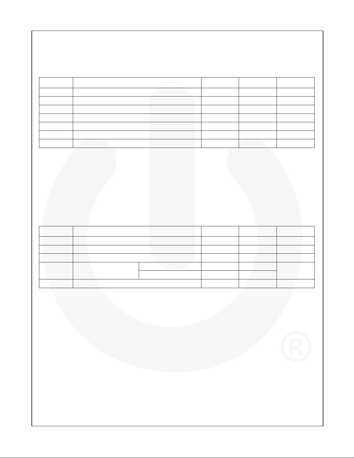
Absolute Maximum Ratings
Stresses exceeding the absolute maximum ratings may damage the device. The device may not function or be
operable above the recommended operating conditions and stressing the parts to these levels is not recommended.
In addition, extended exposure to stresses above the recommended operating conditions may affect device reliability.
The absolute maximum ratings are stress ratings only.
Symbol Parameter Min. Max. Unit
VCC Supply Voltage -0.5 7.0 V
VS DC Switch Voltage -0.5 7.0 V
VIN DC Input Voltage
IIK DC Input Diode Current, VIN<0V -50 mA
I
DC Output Sink Current 128 mA
OUT
ICC / I
DC V
GND
T
Storage Temperature Range -65 +150 °C
STG
/ GND Current ±100 mA
CC
Note:
1. The input and output negative voltage ratings may be exceeded if the input and output diode current ratings are
observed.
(1)
-0.5 7.0 V
Recommended Operating Conditions
The Recommended Operating Conditions table defines the conditions for actual device operation. Recommended
operating conditions are specified to ensure optimal performance to the datasheet specifications. Fairchild does not
recommend exceeding them or designing to Absolute Maximum Ratings.
Symbol Parameter Min. Max. Unit
VCC Power Supply Operating 4.5 5.5 V
VIN Input Voltage 0 5.5 V
V
Output Voltage 0 5.5 V
OUT
tr, tf Input Rise and Fall Time
Switch Control Input
Switch I/O 0 DC
TA Operating Temperature, Free Air -40 +85 °C
Note:
2. Unused control inputs must be held HIGH or LOW. They may not float.
(2)
0 5
ns/V
© 2001 Fairchild Semiconductor Corporation www.fairchildsemi.com
FST3D125 • Rev. 1.0.3 3
Page 4

DC Electrical Characteristics
Typical values are at V
Symbol Parameter Condition VCC (V)
VIK Clamp Diode Voltage I
VIH High-Level Input Voltage 4.5 to 5.5 2.0 V
VOH High-Level
VIL Low-Level Input Voltage 4.5 to 5.5 0.8 V
IIN Input Leakage Current
IOZ Off-state Leakage Current
RON Switch On Resistance
ICC Quiescent Supply Current
ΔICC
Note:
3. Measured by the voltage drop between the A and B pins at the indicated current through the switch. On
resistance is determined by the lower of the voltages on the A or B pins.
Increase in ICC per Input
= 5.0V and TA = 25°C.
CC
(3)
T
=-40 to +85°C
A
Min. Typ. Max.
= -18mA 4.5 -1.2 V
IN
Figure 5, Figure 6, and
Figure 7
0 ≤ VIN ≤ 5.5V
VIN = 5.5V
0 ≤ A, B ≤ V
= 0V, IIN = 64mA 4.5 4 7
V
IN
CC
VIN = 0V, IIN = 30mA 4.5 4 7
VIN = 2.4V, IIN = 15mA 4.5 35 50
/OE
= /OE2 = GND
1
V
= VCC or GND,
IN
I
= 0
OUT
/OE1 = /OE2 = VCC
V
= VCC or GND,
IN
I
= 0
OUT
One Input at 3.4V, Other
Inputs at VCC or GND
4.0 to 5.5 V
5.5 ±1.0 µA
0 10 µA
5.5 ±1.0 µA
1.5
5.5
10
5.5 2.5 mA
FSTD3125 — 4-Bit Bus Switch with Level Shifting
Unit
Ω
µA
AC Electrical Characteristics
TA = -40 to +85°C, CL = 50pF, and RU = RD = 500Ω.
V
= 4.5 – 5.5V
Symbol Parameter Condition
CC
Unit Figure
Min. Max.
t
, t
PHL
t
PZH ,tPZL
t
, t
PHZ
Propagation Delay, Bus-to-Bus
PLH
Output Enable Time
Output Disable Time
PLZ
(4)
V
= Open 0.25 ns
IN
= 7V for t
V
IN
V
= Open for t
IN
= 7V for t
V
IN
V
= Open for t
IN
PZL
PLZ
PZH
PHZ
1.0 6.1 ns
1.5 6.4 ns
Note:
4. This parameter is guaranteed by design, but is not tested. The bus switch contributes no propagation delay other
than the RC delay of the typical on resistance of the switch and the 50pF load capacitance when driven by an
ideal voltage source (zero output impedance).
Figure 3
Figure 4
Figure 3
Figure 4
Figure 3
Figure 4
Capacitance
TA = +25°C, f = 1MHz. Capacitance is characterized, but not tested.
Symbol Parameter Condition Typ. Unit
CIN Control Pin Input Capacitance VCC = 5.0V 3 pF
C
Input/Output Capacitance VCC, /OE = 5.0V 6 pF
I/O
© 2001 Fairchild Semiconductor Corporation www.fairchildsemi.com
FST3D125 • Rev. 1.0.3 4
Page 5

AC Loadings and Waveforms
Notes: Input driven by 50Ω source terminated in 50Ω.
includes load and stray capacitance.
C
L
Input PRR = 1.0MHz, t
= 500ns.
w
Figure 3. AC Test Circuit
FSTD3125 — 4-Bit Bus Switch with Level Shifting
Figure 4. AC Waveforms
© 2001 Fairchild Semiconductor Corporation www.fairchildsemi.com
FSTD3125 • Rev. 1.0.3 5
Page 6

Performance Characteristics
Figure 5. Output Voltage vs. Supply Voltage, V
IN
= V
CC, TA
FSTD3125 — 4-Bit Bus Switch with Level Shifting
= 85°C
Figure 6. Output Voltage vs. Supply Voltage, V
IN
= V
CC, TA
= 25°C
Figure 7. Output Voltage vs. Supply Voltage, V
IN
= V
CC, TA
= 0°C
© 2001 Fairchild Semiconductor Corporation www.fairchildsemi.com
FSTD3125 • Rev. 1.0.3 6
Page 7

Physical Dimensions
FSTD3125 — 4-Bit Bus Switch with Level Shifting
0.43 TYP
0.65
1.65
0.45
R0.09 min
6.10
12.00°
TOP & BOTTOM
A. CONFORMS TO JEDEC REGISTRATION MO-153,
VARIATION AB, REF NOTE 6
1.00
R0.09min
B. DIMENSIONS ARE IN MILLIMETERS
C. DIMENSIONS ARE EXCLUSIVE OF BURRS, MOLD FLASH,
AND TIE BAR EXTRUSIONS
D. DIMENSIONING AND TOLERANCES PER ANSI
Y14.5M, 1982
E. LANDPATTERN STANDARD: SOP65P640X110-14M
F. DRAWING FILE NAME: MTC14REV6
Figure 8. 14-Lead, Thin Shrink Small Outline Package (TSSOP) MO-153, 4mm Wide
Package drawings are provided as a service to customers considering Fairchild components. Drawings may change in any manner
without notice. Please note the revision and/or date on the drawing and contact a Fairchild Semiconductor representative to verify or
obtain the most recent revision. Package specifications do not expand the terms of Fairchild’ s worldwide terms and conditions, specifically the
warranty therein, which covers Fairchild products.
Always visit Fairchild Semiconductor’s online packaging area for the most recent package drawings:
http://www.fairchildsemi.com/packaging/
© 2001 Fairchild Semiconductor Corporation www.fairchildsemi.com
FSTD3125 • Rev. 1.0.3 7
Page 8
FSTD3125 — 4-Bit Bus Switch with Level Shifting
© 2001 Fairchild Semiconductor Corporation www.fairchildsemi.com
FSTD3125 • Rev. 1.0.3 8
 Loading...