

Page 1
March 2008
FSUSB31
Low-Power 1-Port Hi-Speed USB 2.0 (480Mbps) Switch
FSUSB31 — Low-Power 1-Port Hi-Speed USB 2.0 (480 Mbps) Switch
Features
■ Low On Capacitance: 3.7pF (Typical)
■ Low On Resistance: 6.5Ω (Typical)
■ Low Power Consumption: 1µA (Maximum)
– 10µA Maximum I
Volt age Range: V
■ Wide -3dB Bandwidth: > 720MHz
■ 8kV I/O to GND ESD Protection
■ Power-off Protection W hen V
Over an Expanded Control
CCT
=
IN
2.6V, V
=
4.3V
CC
= 0V , D+ / D- Pins Can
CC
Tolerate up to 4.3V
■ Packaged in:
– 8-lead MicroPak™ (1.6 x 1.6mm)
– 8-lead US8
– 8-lead Ultrathin MLP (1.2 x 1.4mm)
Applications
■ Cell Phone, PDA, Digital Camera, an d Notebook
■ LCD Monitor, TV, and Set-top Box
Related Resources
■ AN-6022 Using the FSUSB30/31 to Comply with
USB 2.0 Fault Condition Requirements
Description
The FSUSB31 is a low-power, single-port, high-speed
USB 2.0 switch. This p a rt is con figu red as a d oub le-pole,
single-throw switch and is optimized for switching or isolating a high-speed (480Mbps) source or a high-speed
and full-sp eed (12Mb ps) source. T he FSUSB3 1 is compatible with t he r eq uirem ents o f USB 2. 0 and f eat ures an
extremely low on capacitance (C
bandwidth of th is device (>720 MHz) exceeds the bandwidth needed to pass the third harmonic, resulting in signals with minimum edge and phase distortion. Superior
channel-to-channel crosstalk minimizes interference.
The FSUSB31 contains special circuitry on the D+
pins that allows the device to withstand an over-voltage
condition. This device is also designed to minimize current consumption even when the control voltage applied
to the OE
pin is lower than the supply voltage (VCC). This
feature is especially valuable for mobile applications,
such as cell phones, allowing direct interface with the
general-purpose I/Os of the baseband processor. Other
applications include port isolation and switching in portable cell phones, PDAs, digital cameras, printers, and
notebook computers.
) of 3.7pF. The wide
ON
/ D-
Ordering Information
Part Number Package Package Description
FSUSB31K8X MAB08A 8-Lead US8, JEDEC MO-187, Variat ion CA 3.1mm Wide
FSUSB31L8X MAC08A 8-Lead MicroPak, 1.6mm Wide
FSUSB31UMX (Preliminary ) UMLP08A 8-Lead, Ultrathin Mold ed Leadless Package (UMLP), 1.2 x 1.4mm
All packages are lead free per JEDEC: J-STD-020B standard.
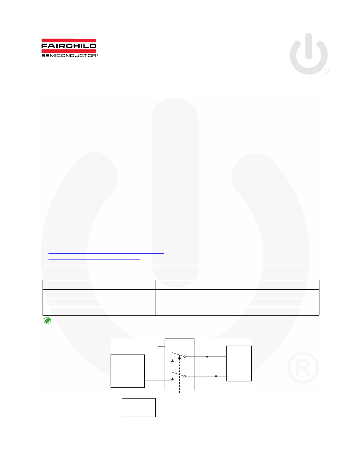
Application Diagram
V
CC
Base Band
Processor
or FS USB
Controller
HS USB
Controller
Figure 1. Typical Application Diagram
MicroPak™ is a trademark of Fairchild Semiconductor Corporation.
© 2006 Fairchild Semiconductor Corporation www.fairchildsemi.com
FSUSB31 Rev. 1.0.7
FSUSB31
OE
D+
D–
USB
Connector
Page 2
FSUSB31 — Low-Power 1-Port Hi-Speed USB 2.0 (480 Mbps) Switch
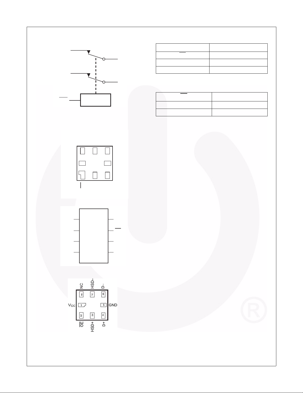
Analog Symbol
HSD+
HSD–
OE
Figure 2. Analog Symbol
Control
Connection Diagrams
NC
7 65
V
CC
13
HSD–
2
Pin Descriptions
Pin Name Description
D+
D+, D−, HSD+, HSD− Data Ports
OE Bus Switch Enable
NC No Connect
D–
Truth Table
OE
HIGH Disconnect
LOW D+, D− = HSD+, HSD-
D–
48
GND
Function
OE
D+
HSD+
Figure 3. Pin Assignments for MicroPak
NC
HSD–
D–
GND
1
2
3
4
8
V
CC
7
OE
6
HSD+
5
D+
Figure 4. Pin Assignments for US8
Figure 5. Pin Assignments for UMLP
© 2006 Fairchild Semiconductor Corporation www.fairchildsemi.com
FSUSB31 Rev. 1.0.7 2
Page 3
Absolute Maximum Ratings
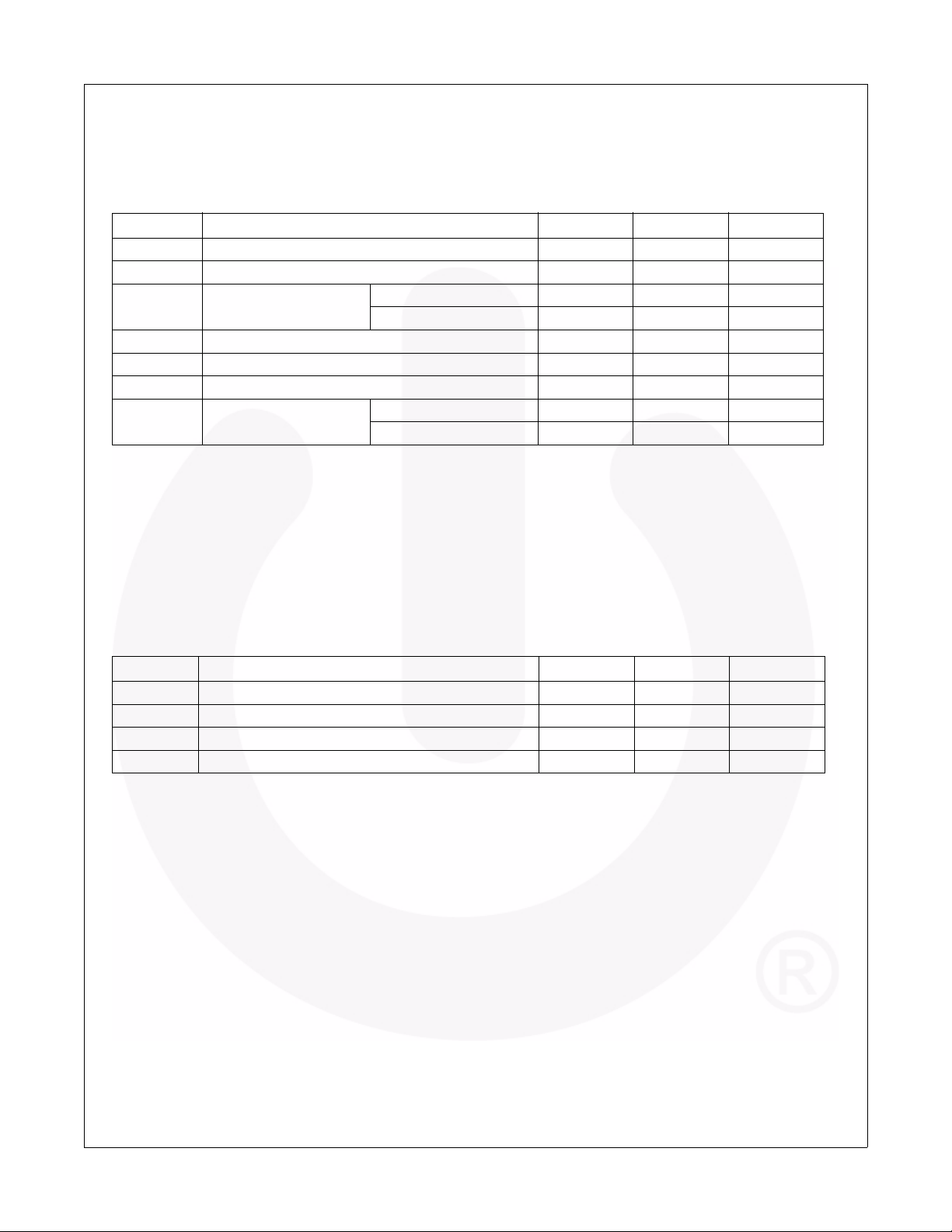
Stresses exceeding the absolute maximum ratings may damage the device. The device may not function or be operable above the recommend ed op erati ng cond iti ons and stres si ng the p arts to these levels is not reco mm en ded. In addition, extended exposure to stresses above the recommended operating conditions may affect device reliability. The
absolute maximum ratings are stress ratings only.
Symbol Parameter Minimum Maximum Unit
V
CC
V
S
V
IN
I
IK
I
OUT
T
STG
ESD Human Body Model
Note:
1.The input and output negative voltage ratings may be exceeded if the input and output diode current ratings are
observed. DC swit ch vo ltage may never exce ed 4.6 V.
Supply Voltage -0.5 4.6 V
DC Input Voltage
DC Switch Voltage
(1)
(1)
-0.5 4.6 V
HSD -0.5 VCC+0.3 V
D+, D− -0.5 +4.6 V
DC Input Diode Current -50 mA
DC Output Current 50 mA
Storage Temperature -65 +150 °C
All Pins 7.5 kV
I/O to GND 8 kV
FSUSB31 — Low-Power 1-Port Hi-Speed USB 2.0 (480 Mbps) Switch
Recommended Operating Conditions
The Recommended Operating Conditions table defines the conditions for actual device operation. Recommended
operating conditions are specified to ensure optimal performance to the datasheet specifications. Fairchild does not
recommend exceeding them or designing to absolute maximum ratings.
Symbol Parameter Minimum Maximum Unit
V
CC
V
IN
T
A
Note:
2. Control input must be held HIGH or LOW and it must not float.
Supply V oltage 3.0 4.3 V
Control Input Voltage
Switch Input Voltage 0 V
(2)
0 VCC V
CC
V
Operating Temperature -40 +85 °C
© 2006 Fairchild Semiconductor Corporation www.fairchildsemi.com
FSUSB31 Rev. 1.0.7 3
Page 4
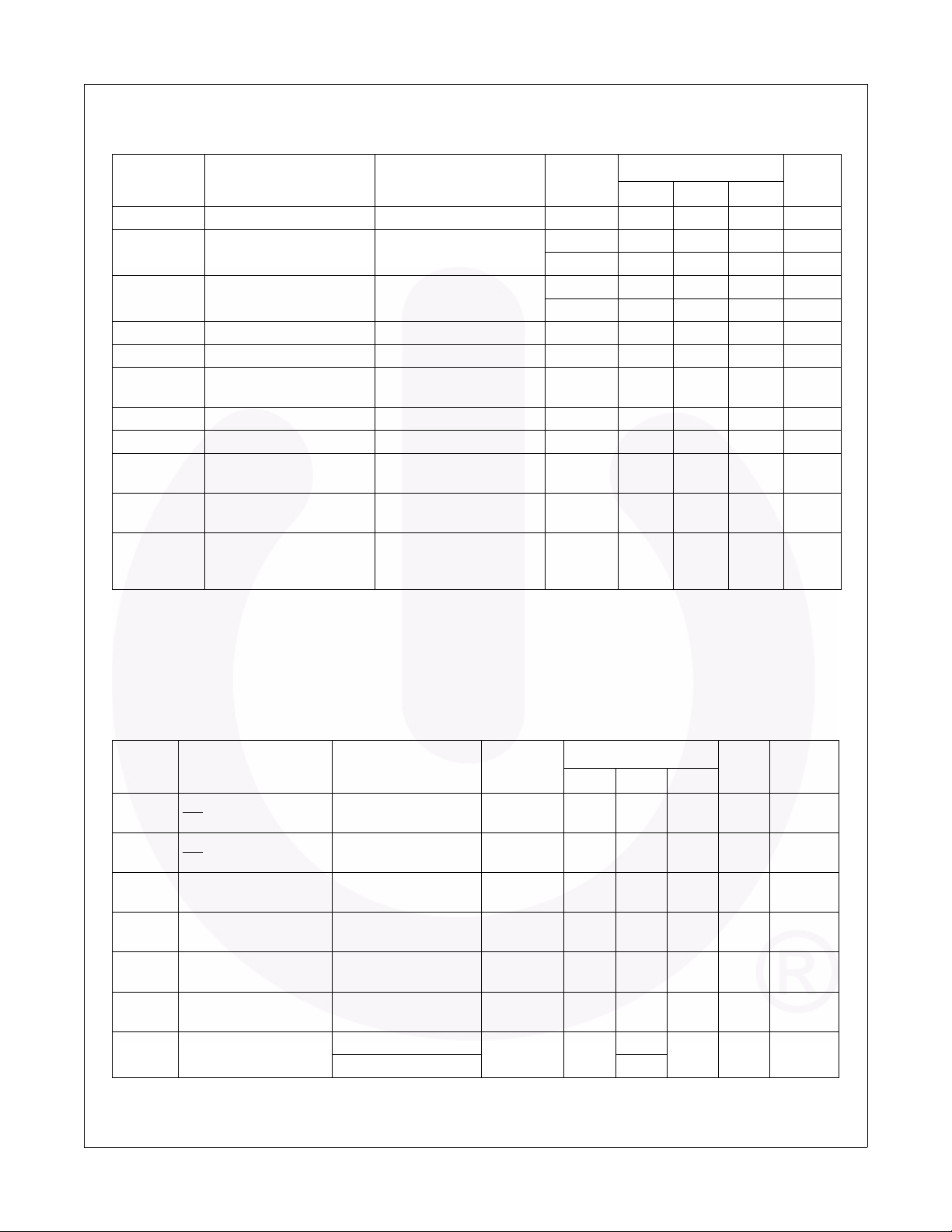
DC Electrical Characteristics
All typical values are at 25°C unless otherwise specified.
T
= −40°C to +85°C
V
Symbol Parameter Conditions
V
IK
V
IH
V
IL
I
IN
I
OZ
I
OFF
R
ON
ΔR
ON
Flatness RON Flatness
R
ON
I
CC
Clamp Diode Voltage IIN = −18mA 3.0 -1.2 V
Input Voltage HIGH
Input Voltage LOW
Control Input Leakage VIN = 0V to V
OFF State Leakage 0 ≤ HSD ≤ V
Power OFF Leakage
Current (D+, D–)
Switch On Resistance
ON
(4)
(3)
Delta R
Quiescent Supply Current
VIN = 0.0V to 4.3V,
= 0V
V
CC
(3)
VIN = 0.4V, ION = −8mA 3.0 6.5 10.0 Ω
VIN = 0.4V, ION = −8mA 3.0 0.35 Ω
VIN = 0.0V −1.0V,
= −8mA
I
ON
= 0.0V or VCC,
V
IN
= 0
I
OUT
CC
CC
(V)
CC
3.0 to 3.6 1.3 V
4.3 1.7
3.0 to 3.6 0.5 V
4.3 0.7
4.3 -1.0 1.0 μA
4.3 -2.0 2.0 μA
0-2.0 2.0μA
3.0 2.0 Ω
4.3 1.0 μA
Increase in ICC Current
I
CCT
per Control Voltage and
Levels
V
CC
V
= 2.6V, VCC = 4.3V 4.3 10.0 μA
IN
Notes:
3. Measured by the voltage drop between Dn, HSD, and Dn pins at the indicated current through the switch.
On resistance is determined by the lower of the voltage on the two ports.
4. Guaranteed by characterization.
A
Min. Typ. Max.
FSUSB31 — Low-Power 1-Port Hi-Speed USB 2.0 (480 Mbps) Switch
Unit
AC Electrical Characteristics
All typical values are for VCC = 3.3V are at 25°C unless otherwise specified.
T
= −40°C to +85°C
Symbol Parameter Conditions
t
t
OFF
t
t
BBM
O
Xtalk
Turn-On Time,
ON
to Output
OE
Turn-Off Time,
to Output
OE
Propagation Delay
PD
Break-Before-Make
Off Isolation
IRR
(Non-Adjacent)
Non-Adjacent Channel
Crosstalk
BW -3dB Bandwidth
V
= 0.8V, RL = 50Ω,
IN
= 5pF
C
L
V
= 0.8V, RL = 50Ω,
IN
= 5pF
C
L
(5)
RL = 50Ω, CL = 5pF 3.3 0.25 ns
= 50Ω, CL = 5pF,
R
L
= 0.8V
V
IN
= 50Ω, f = 240MHz 3.0 to 3.6 -35.0 dB Figure 17
R
T
= 50Ω, f = 240MHz 3.0 to 3.6 -55.0 dB Figure 18
R
T
= 50Ω, CL = 0pF
R
T
R
= 50Ω, CL = 5pF 550
T
V
(V)
CC
3.0 to 3.6 15.0 30.0 ns Figure 13
3.0 to 3.6 12.0 25.0 ns Figure 13
3.0 to 3.6 2.0 6.5 ns Figure 14
3.0 to 3.6
A
Min. Typ. Max.
720
Unit
MHz Figure 16
Note:
5. Guaranteed by characterization.
© 2006 Fairchild Semiconductor Corporation www.fairchildsemi.com
FSUSB31 Rev. 1.0.7 4
Figure
Number
Figure 11
Figure 12
Page 5
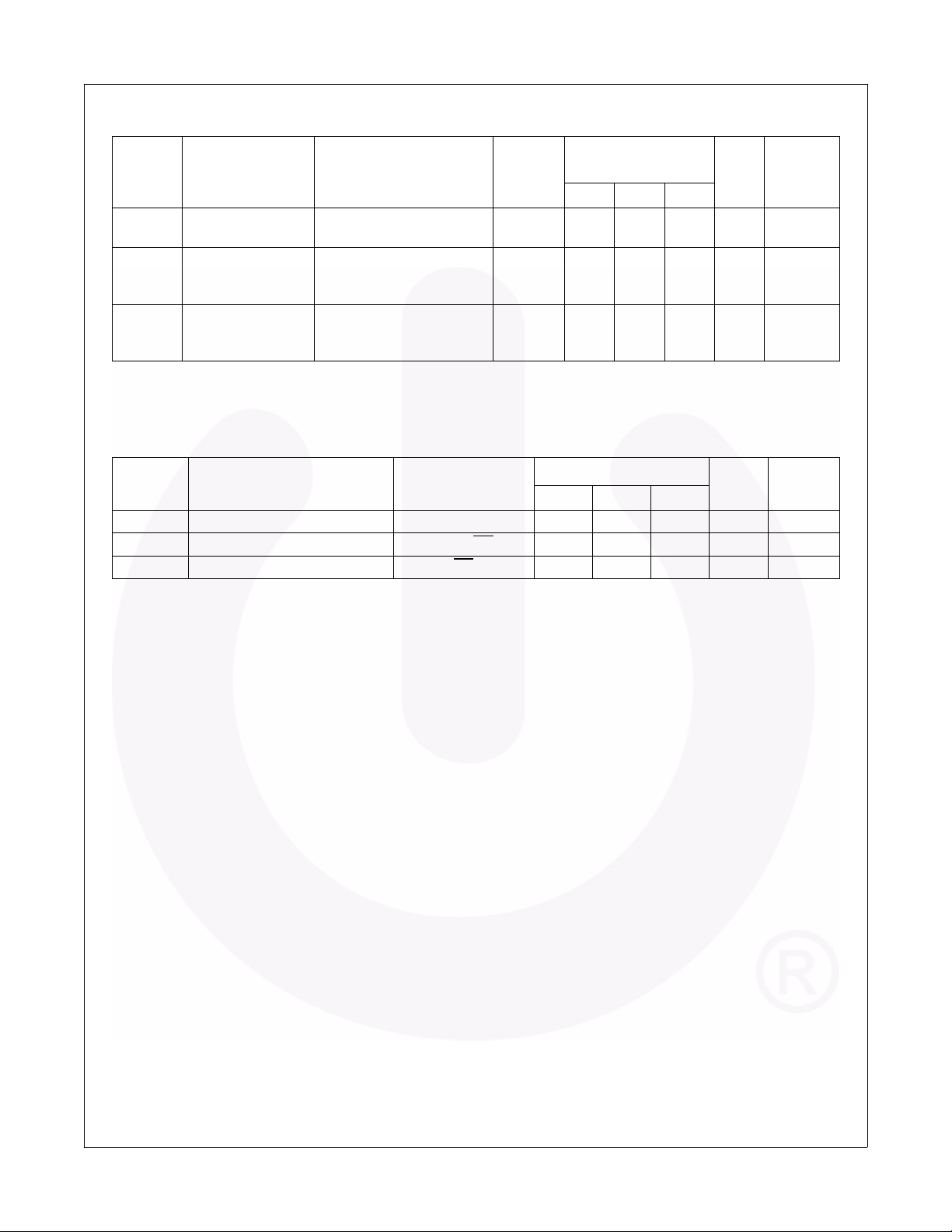
USB Hi-Speed Related AC Electrical Characteristics
(V)
Symbol Parameter Conditions
t
SK(O)
t
SK(P)
Channel-to-Channel Skew
Skew of Opposite
Transi tions of the
Same Output
Total Jitter
t
J
(6)
(6)
(6)
CL = 5pF 3.0 to 3.6 50.0 ps
CL = 5pF 3.0 to 3.6 20.0 ps
RL = 50Ω, CL = 5pF,
= tF = 500ps at 480 Mb ps
t
R
(PRBS = 2
15
− 1)
V
CC
3.0 to 3.6 200 ps
Note:
6.Guaranteed by design.
Capacitance
Symbol Parameter Conditions
C
C
C
OFF
Control Pin Input Capacitance VCC = 0V 1.0 pF Figure 20
IN
On Capacitance VCC = 3.3V, OE = 0V 3.7 pF Figure 19
ON
Off Capacitance VCC and OE = 3.3V 1.7 pF Figure 20
T
Min. Typ. Max.
= −40°C to
T
A
+85°C
Min. Typ. Max.
= −40°C to +85°C
A
Unit
Unit
FSUSB31 — Low-Power 1-Port Hi-Speed USB 2.0 (480 Mbps) Switch
Figure
Number
Figure 11
Figure 15
Figure 11
Figure 15
Figure
Number
© 2006 Fairchild Semiconductor Corporation www.fairchildsemi.com
FSUSB31 Rev. 1.0.7 5
Page 6
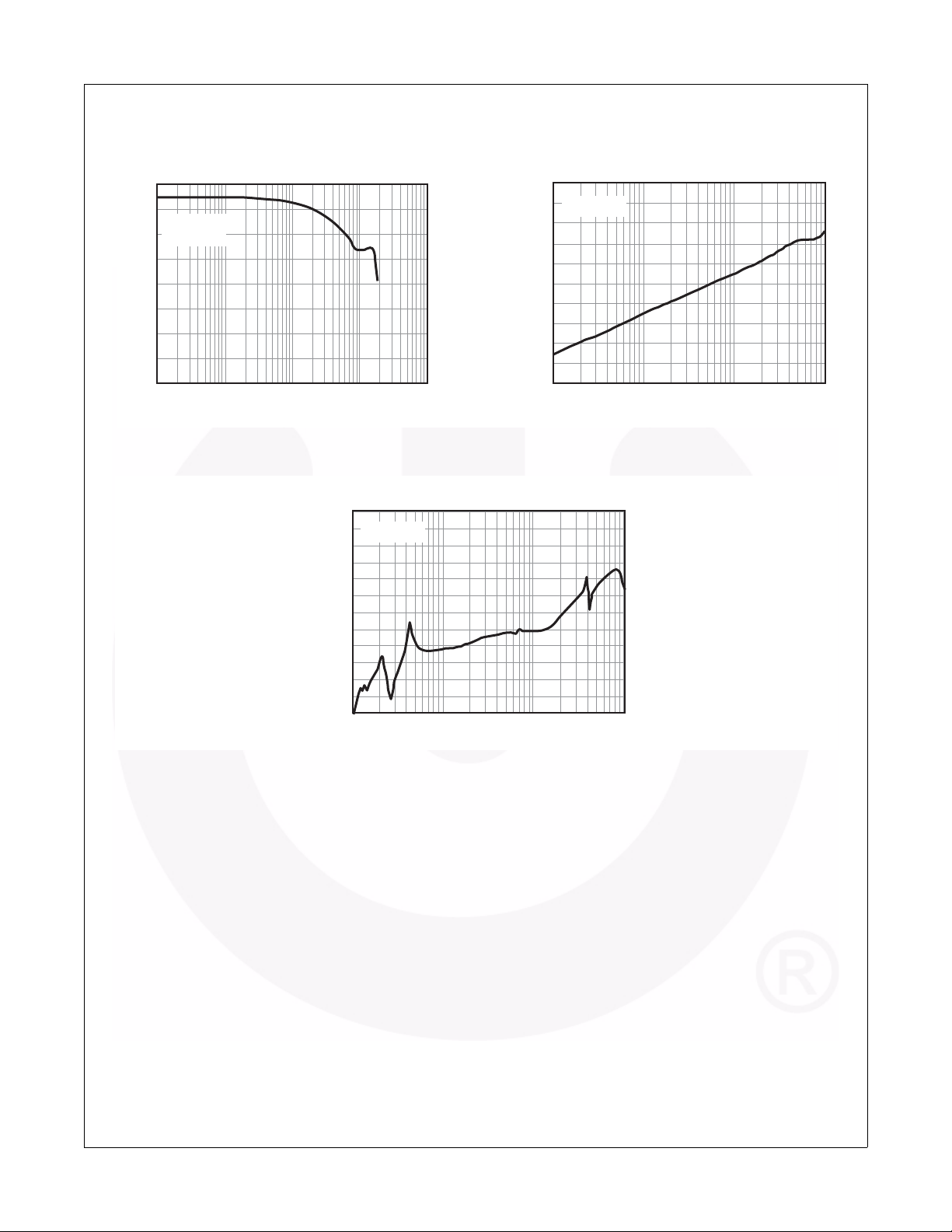
Ty pical Characteristics
FSUSB31 — Low-Power 1-Port Hi-Speed USB 2.0 (480 Mbps) Switch
0
-1
CL = 0pF
-2
= 3.3V
V
CC
-3
-4
Gain (dB)
-5
-6
-7
-8
1 10 100 1000 10000
Frequency (MHz)
Figure 6. Gain vs. Frequency Figure 7. Off Isolation
0
-10
VCC = 3.3V
-20
-30
-40
-50
-60
-70
-80
Crosstalk (dB)
-90
-100
-110
-120
1 10 100 1000
-10
-20
-30
-40
-50
-60
-70
Off Isolation (dB)
-80
-90
-100
Frequency (MHz)
0
VCC = 3.3V
1 10 100 1000
Frequency (MHz)
Figure 8. Crosstalk
© 2006 Fairchild Semiconductor Corporation www.fairchildsemi.com
FSUSB31 Rev. 1.0.7 6
Page 7
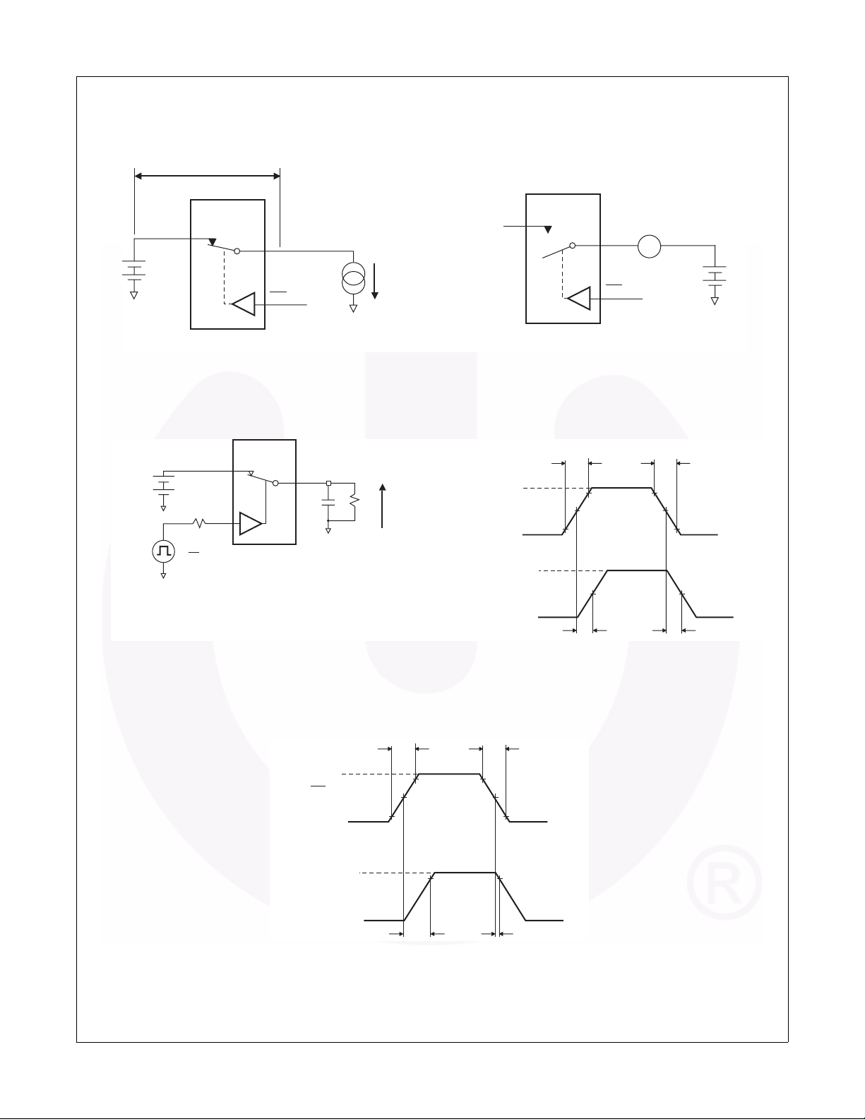
Test Diagrams
V
FSUSB31 — Low-Power 1-Port Hi-Speed USB 2.0 (480 Mbps) Switch
ON
FSUSB31
HSD
Dn
V
GND
IN
OE
= 0 to V
V
S
ON
CC
GND
I
ON
Figure 9. On Resistance Figure 10. Off Leakage
FSUSB31
HSD
V
IN
GND
R
S
V
OE
GND
RL, RS, and CL are functions of the application environment
(see AC Electrical tables for specific values).
*CL includes test fixture and stray capacitance.
D+, D–
CL*
GND
V
R
L
OUT
NC
t
RISE
800mV
HSD+,
Input:
HSD–
400mV
Output: D+, D–
FSUSB31
OE
VS = 0 or V
Each switch port is tested separately.RON = VON / I
= 500ps
90%
50% 50%
10% 10%
V
OH
50%
V
OL
t
PLH
ID
n(OFF)
A
90%
CC
50%
t
FALL
t
PHL
V
IN
GND
= 500ps
Figure 11. AC Test Circuit Load Figure 12. Switch Propagation Delay Waveforms
(tPD)
t
t
OFF
FALL
ON
= 2.5ns
/ t
OFF
)
t
= 2.5ns
RISE
V
Input – OE
Output – V
CC
GND
OUT
10% 10%
V
OH
V
OL
90%
V
/2 VCC/2
CC
t
ON
90%
90%90%
Figure 13. Turn On / Turn Off Waveform (t
© 2006 Fairchild Semiconductor Corporation www.fairchildsemi.com
FSUSB31 Rev. 1.0.7 7
Page 8
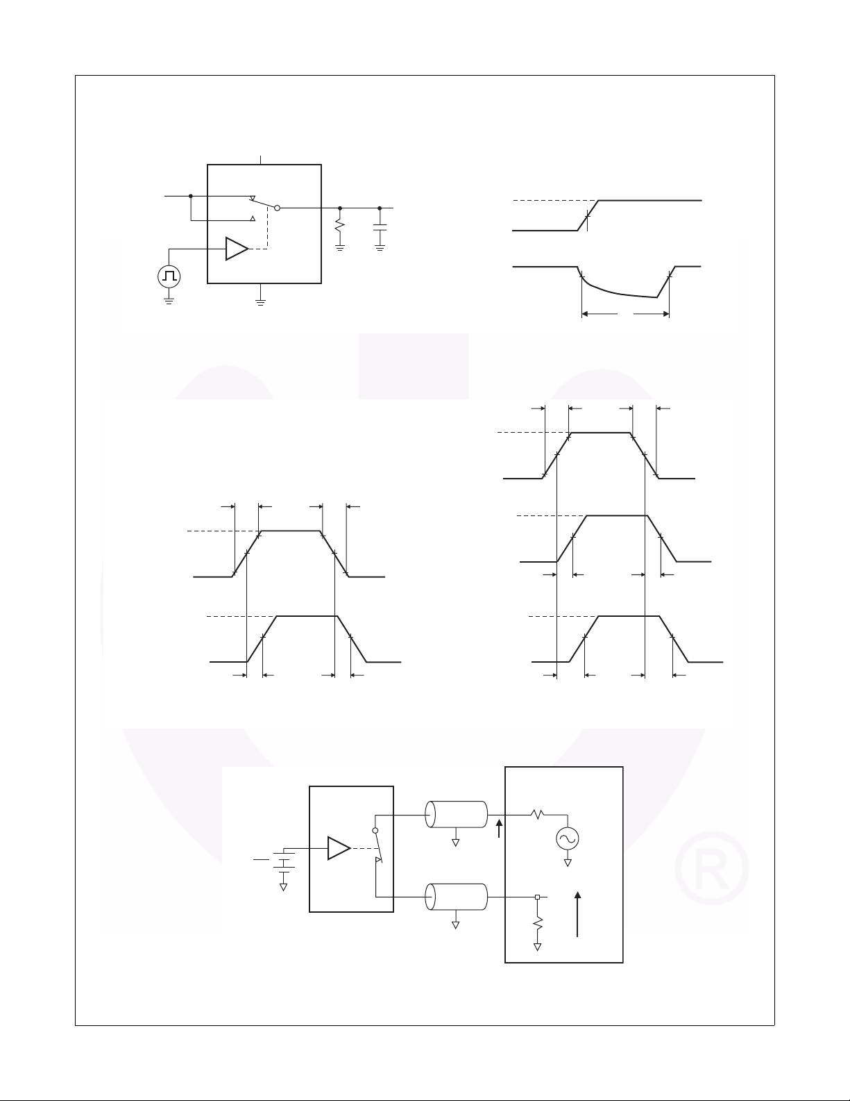
Test Diagrams (Continued)
V
CC
V
CC
V
O
Control
Input
*CL includes test fixture and stray capacitance.
HSDn
D+, D–
HSDn
S
GND
FSUSB31 — Low-Power 1-Port Hi-Speed USB 2.0 (480 Mbps) Switch
V
OUT
R
C
L
L
Control
Input
*
V
CC
0V
V
OUT
50%
tR = tF = 2.5ns (10–90%)
0.9 x V
t
D
OUT
t
800mV
nput:
HSDn+
HSDn–
400mV
utput: D+, D–
RISE
= 500ps
V
OH
V
OL
90% 90%
50%
10%
T
= | t
SK(P)
Pulse Skew, T
50%
PHL
t
Figure 14. Break-Before-Make (t
= 500ps
t
FALL
50%
10%
50%
PLH
– t
SK(P)
PLH
|
t
PHL
Figure 15. Switch Skew Tests
t
= 500ps
RISE
800mV
Input: D+, D–
400mV
V
Output1:
HSD1+
HSD1–
V
OL
Output1: D2+, D2–
)
BBM
10%
OH
V
OH
V
OL
T
= | t
SK(O)
Output Skew, T
90% 90%
50%
50%
t
PLH1
50%
t
– t
PLH1
SK(OUT)
PLH2
PLH2
50%
| or | t
10%
PHL1
50%
t
FALL
t
– t
50%
= 500ps
PHL1
t
PHL2
PHL2
|
Network Analyzer
FSUSB31
GND
V
OE
R
S
V
IN
V
S
GND
GND
V
OUT
T
GND
RS and RT are functions of the application environment
(see AC Electrical Tables for specific values).
R
GND
Figure 16. Bandwidth
© 2006 Fairchild Semiconductor Corporation www.fairchildsemi.com
FSUSB31 Rev. 1.0.7 8
Page 9
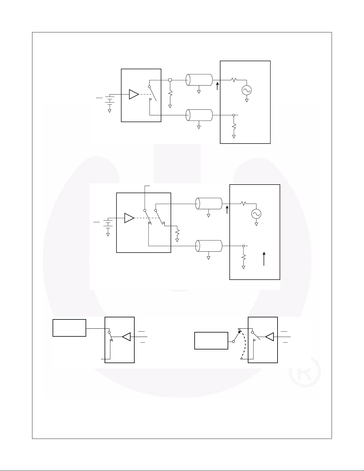
Test Diagrams (Continued)
V
OE
GND
OFF-Isolation = 20 Log (V
FSUSB31
R
T
GND
VIN)
OUT
/
Figure 17. Channel Off Isolation
GND
GND
Network Analyzer
R
S
V
IN
V
GND
V
OUT
R
T
GND
FSUSB31 — Low-Power 1-Port Hi-Speed USB 2.0 (480 Mbps) Switch
S
Capacitance
Meter
F = 240MHz
V
OE
GND
HSDn
NC
FSUSB31
GND
R
T
GND
GND
and RT are functions of the application environment
R
S
(50, 75 or 100Ω).
Crosstalk = 20 Log (V
OUT
/ VIN)
Figure 18. Non-Adjacent Channel-to-Channel Crosstalk
FSUSB31
Dn
OE
V
OE
= 0 or V
CC
Capacitance
Meter
F = 240MHz
Network Analyzer
R
S
V
IN
V
GND
R
T
GND
FSUSB31
Dn
HSDn
S
V
OUT
OE
VOE = 0 or V
CC
Figure 19. Channel On Capacitance Figure 20. Channel Off Capacitance
© 2006 Fairchild Semiconductor Corporation www.fairchildsemi.com
FSUSB31 Rev. 1.0.7 9
Page 10
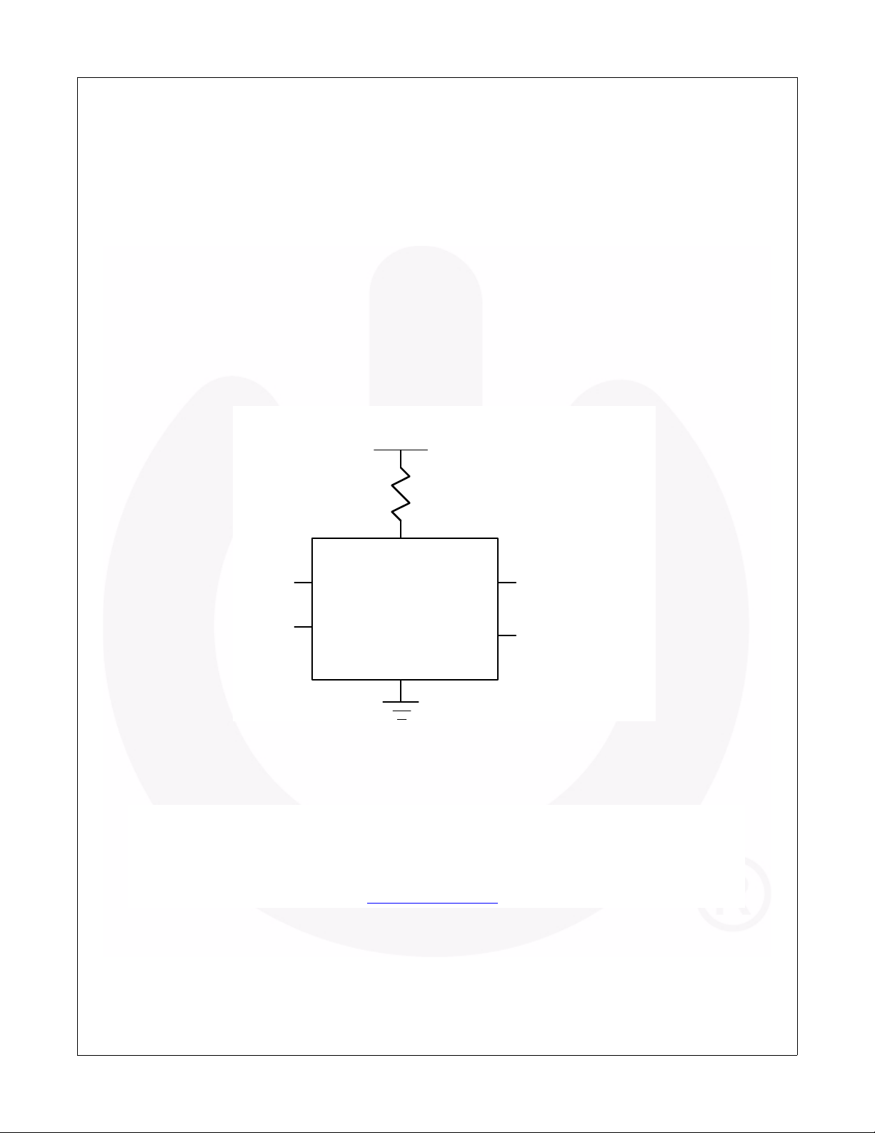
Application Guidance: Meeting USB 2.0 Vbus Short Requirements
FSUSB31 — Low-Power 1-Port Hi-Speed USB 2.0 (480 Mbps) Switch
In section 7.1.1 of the USB 2.0 specification, it notes that
USB devices must be able to withstand a Vbus short to
D+ or D- when the USB devices is either powered off or
powered on. The FSUSB31 can be successfully configured to meet both these requirements.
Power-Off Protection
For a Vbus short circuit, the switch is expected to withstand such a condition for at least 24 hours. The
FSUSB31 has specially designed circuitry which prevents unintended signal bleed through as well as guaranteed system reliability during a power-down, overvoltage condition. The protection has been added to the
common pins (D+, D-).
VCC= 3.6 V
100 Ohms
Power-On Protection
The USB 2.0 specification also notes that the USB
device shoul d be capable of withs tanding a Vbus short
during transmission of data. Fairchild recommends adding a 100Ω series resister between the switch VCC pin
and supply rail to protect against this case. This modification works by limiting current flow back into the VCC
rail during the over-voltage event so current remains
within th e safe operati ng range. In this applicat ion, the
switch passes the full 5.25V input signal through to the
selected output, while maintaining specified off isolation
on the un-selected pins.
HSD+
D+ = 5.25V
FSUSB31
HSD-
Figure 21. A 100Ω resistor in series with the VCC supply allows the FSUSB31 to withstand a Vbus
short when powered up
For more information, see Applications Note AN-6022 — Using the FSUSB30/FSUSB31 to Comply with
USB 2.0 Fault Condition Requirements at www.fairchildsemi.com
D- = 5.25V
.
© 2006 Fairchild Semiconductor Corporation www.fairchildsemi.com
FSUSB31 Rev. 1.0.7 10
Page 11
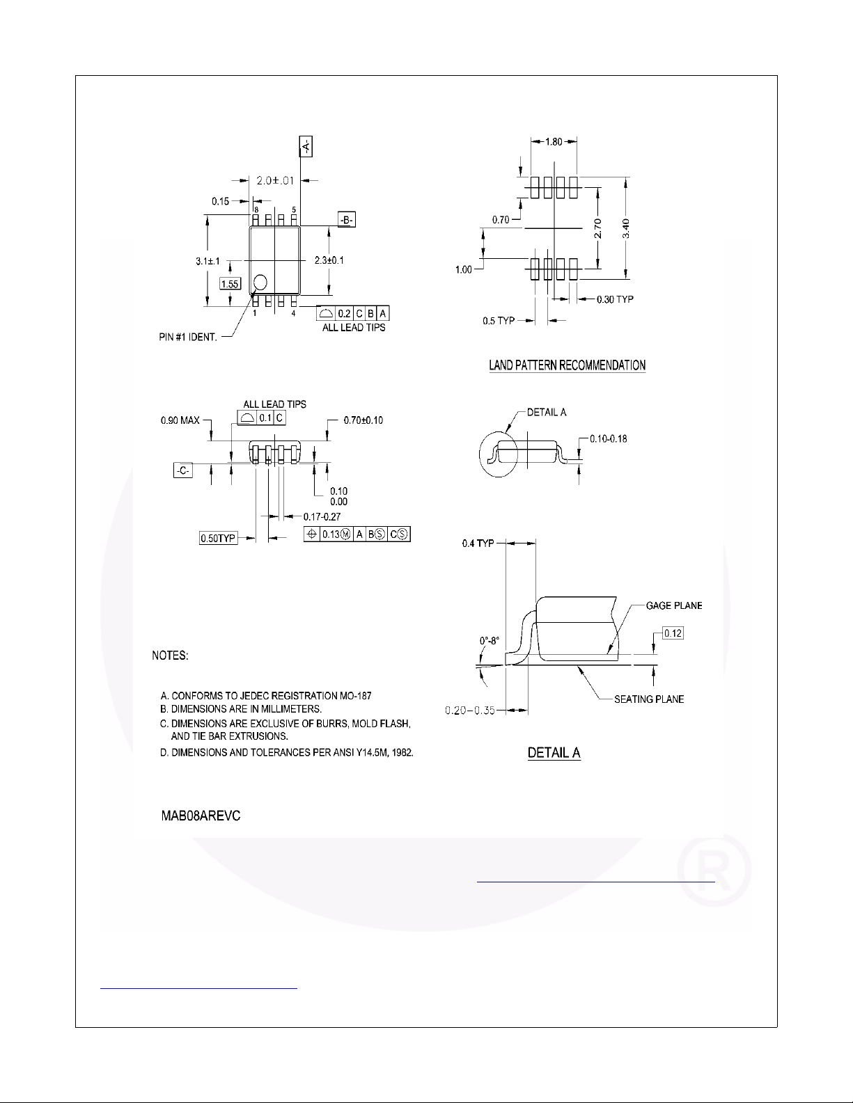
Physical Dimensions
FSUSB31 — Low-Power 1-Port Hi-Speed USB 2.0 (480 Mbps) Switch
Figure 22. 8-Lead US8, JEDEC MO-187, Variation CA 3.1mm Wide
For MicroPak™ tape and reel specifications, please visit Fairchild’s website: http://www.fairchildsemi.com/ms/MS/MS-522.pdf
Package drawings are provided as a service to customers considering Fairchild com ponents. Drawings may change in any manner
without notice. Please note the revision and/or date on the drawing and contact a Fairchild Semic onduct or representative to verify or
obtain the most recent revision. Package specifications do not expand the terms of Fairchild’s worldwide terms and conditions, specifically the warranty therein, which covers Fairchild products.
Always visit Fairchild Semiconductor’s online packaging area for the most recent package drawings:
http://www.fairchildsemi.com/packaging/
© 2006 Fairchild Semiconductor Corporation www.fairchildsemi.com
FSUSB31 Rev. 1.0.7 11
Page 12
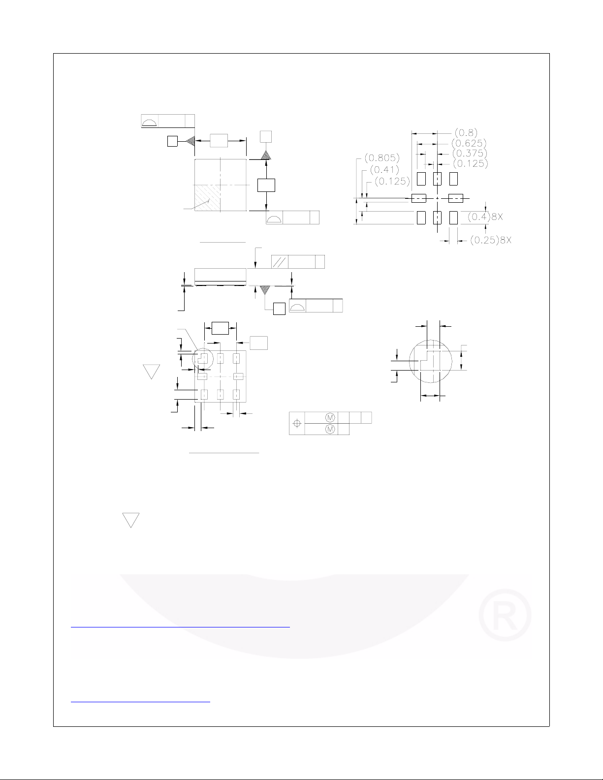
Physical Dimensions (Continued)
FSUSB31 — Low-Power 1-Port Hi-Speed USB 2.0 (480 Mbps) Switch
2X
0.10
INDEX AREA
0.05
0.00
DETAIL A
(0.09)
8X
(0.1)
4
0.35
8X
0.25
(0.2)
3X
C
B
TOP VIEW
1
8
BOTTOM VIEW
1.6
1.0
23
567
2X
0.5
4
0.15
0.25
A
1.6
0.55 MAX
C
8X
C
0.10
0.05 C
0.05
0.10 CAB
0.05
Recommended Landpattern
C
(0.20)
0.35
0.25
(0.15)
0.35
0.25
DETAIL A
C
PIN #1 TERMINAL
SCALE: 2X
Notes:
1. PACKAGE CONFORMS TO JEDEC MO-255 VARIATION UAAD
2. DIMENSIONS ARE IN MILLIMETERS
3. DRAWING CONFORMS TO ASME Y.14M-1994
4. PIN 1 FLAG, END OF PACKAGE OFFSET
5. DRAWING FILE NAME: MKT-MAC08AREV4
MAC08AREV4
Figure 23. 8-Lead MicroPak, 1.6mm Wide
For MicroPak™ tape and reel specifications, please visit Fairchild’s website:
http://www.fairchildsemi.com/products/logic/pdf/micropak_tr.pdf
Package drawings are provided as a service to customers considering Fairchild com ponents. Drawings may change in any manner
without notice. Please note the revision and/or date on the drawing and contact a Fairchild Semic onduct or representative to verify or
obtain the most recent revision. Package specifications do not expand the terms of Fairchild’s worldwide terms and conditions, specifically the warranty therein, which covers Fairchild products.
Always visit Fairchild Semiconductor’s online packaging area for the most recent package drawings:
http://www.fairchildsemi.com/packaging/
© 2006 Fairchild Semiconductor Corporation www.fairchildsemi.com
FSUSB31 Rev. 1.0.7 12
Page 13
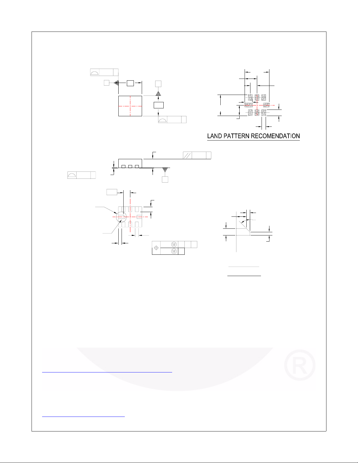
Physical Dimensions (Continued)
FSUSB31 — Low-Power 1-Port Hi-Speed USB 2.0 (480 Mbps) Switch
2X
C
0.05
DETAIL A
PIN#1 IDENT
0.10
B
0.025
0.00
0.40
C
1.4
TOP VIEW
2
1
8
(0.2)
1.450
1.250
0.625
0.30
0.20
0.725
0.400
0.450
0.350 7X
0.250 8X
0.10
45°
0.10
A
1.20
C
2X
4
5
6
0.10
0.55 MAX
SEATING
PLANE
C
0.35
7X
0.25
0.15
8X
0.25
0.10 CAB
0.05
0.05
C
C
BOTTOM VIEW
DETAIL: A
SCALE : 2x
NOTES:
A. DOES NOT CONFORMS TO JEDEC STANDARD.
B. DIMENSIONS ARE IN MILLIMETERS.
C. DIMENSIONS AND TOLERANCES CONFORMS TO ASME Y14.5M, 1994.
D. DRAWING FILE NAME : UMLP08Arev1
Figure 24. 8-Lead, Ultrathin Molded Leadless Package (UMLP), 1.2 x 1.4mm
For MicroPak™ tape and reel specifications, please visit Fairchild’s website:
http://www.fairchildsemi.com/products/logic/pdf/micropak_tr.pdf
Package drawings are provided as a service to customers considering Fairchild com ponents. Drawings may change in any manner
without notice. Please note the revision and/or date on the drawing and contact a Fairchild Semic onduct or representative to verify or
obtain the most recent revision. Package specifications do not expand the terms of Fairchild’s worldwide terms and conditions, specifically the warranty therein, which covers Fairchild products.
Always visit Fairchild Semiconductor’s online packaging area for the most recent package drawings:
http://www.fairchildsemi.com/packaging/
© 2006 Fairchild Semiconductor Corporation www.fairchildsemi.com
FSUSB31 Rev. 1.0.7 13
Page 14
FSUSB31 — Low-Power 1-Port Hi-Speed USB 2.0 (480 Mbps) Switch
© 2006 Fairchild Semiconductor Corporation 14 www.fairchildsemi.com
FSUSB31 Rev. 1.0.7
 Loading...