

Datasheet FSTU3257QSCX, FSTU3257QSC, FSTU3257MX, FSTU3257MTCX, FSTU3257MTC Datasheet (Fairchild Semiconductor)
Page 1
© 2000 Fairchild Semiconductor Corporation DS500302 www.fairchildsemi.com
August 1999
Revised April 2000
FSTU3257 Quad 2:1 Multiplexer/Demultiplexer Bus Switch with −2V Undershoot Protection
FSTU3257
Quad 2:1 Multiplexer/Demultiplexer Bus Switch
with −2V Undershoot Protection
General Description
The Fairchild Swit ch FSTU3257 is a quad 2:1 h igh-speed
CMOS TTL-compatible multiplexer/demultiplexer bus
switch. The low on resistance of the switch allows inputs to
be connected to outputs wi thout a dding pr opagation delay
or generating additional ground bounce noise.
When OE
is LOW, the select pin connects the A Port to the
selected B Port output. The A and B Ports are “undershoot
hardened” with UHC pro tection to support an extended
range of 2.0V below groun d. Fairchild’s integrated Undershoot Hardened Circuit UHC senses undershoot at the I/O
and responds by preventing voltage differentials from
developing and turning on the switch. When OE
is HIGH,
the switch is OPEN and a high-impedance state exists
between the two ports.
Features
■ Undershoot hardened to −2V (A and B Ports)
■ Soft enable turn-on to minimize bus to bus charge
sharing during enable
■ 4Ω switch connection between two ports.
■ Minimal propagation delay through the switch.
■ Low l
CC
.
■ Zero bounce in flow-through mode.
■ Control inputs compatible with TTL level.
■ See Applications Note AN-5008 for details
Ordering Code:
Device also available in Tape and Reel. Specify by appending suffix letter “X” to the ordering code.
UHC is a trademark of Fairchild Semiconductor Corporation.
Order Number Package Number Package Description
FSTU3257M M16A 16-Lead Small Outline Integrated Circuit (SOIC), JEDEC MS-012, 0.150 Narrow
FSTU3257QSC MQA16 16-Lead Quarter Size Outline Package (QSOP), JEDEC MO-137, 0.150 Wide
FSTU3257MTC MTC16 16-Lead Thin Shrink Small Outline Package (TSSOP), JEDEC MO-153, 4.4mm Wide
Page 2
www.fairchildsemi.com 2
FSTU3257
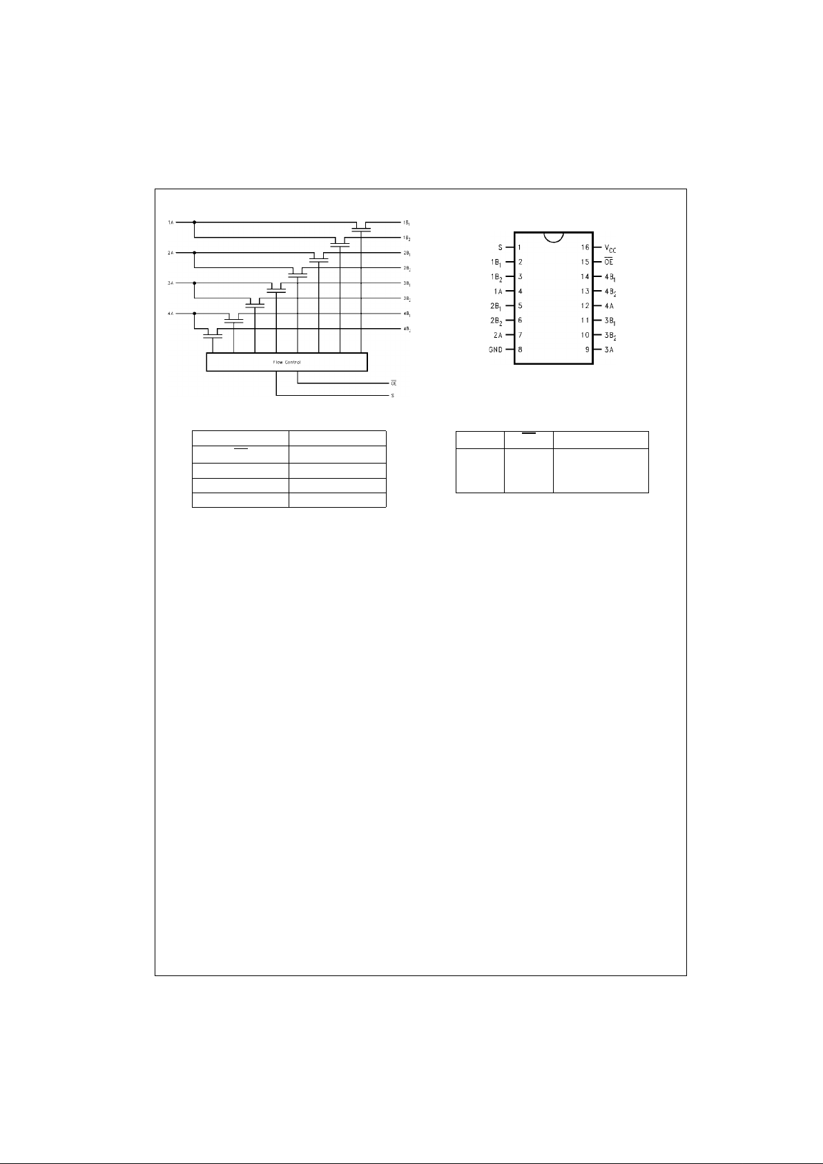
Logic Diagram
Pin Descriptions
Connection Diagram
Tr uth Table
Pin Name Description
OE
Bus Switch Enable
S Select Input
ABus A
B
1–B2
Bus B
SOE Function
X H Disconnect
LL A = B
1
HL A = B
2
Page 3
3 www.fairchildsemi.com
FSTU3257
Absolute Maximum Ratings(Note 1) Recommended Operating
Conditions
(Note 4)
Note 1: The Absolute Maxi mum Ratings are those v alues beyond which
the safety of the dev ice cannot b e guaranteed . The device sh ould not be
operated at these limit s. The parametric values defi ned in the Electrical
Characteristics tables are not guaranteed at the absolute maximum rating.
The Recommend ed Oper ating Condi tions ta bles will de fine the conditions
for actual device operation.
Note 2: V
S
is the volt age observed/applied at either t he A or B Por t s across
the switch.
Note 3: The input and output negative voltage ratings may be exceeded if
the input and ou t put diode curr ent ratings ar e observed.
Note 4: Unused control inputs must be held HIGH or LOW. They may not
float.
DC Electrical Characteristics
Note 5: Typical values are at VCC = 5.0V and TA = +25°C
Note 6: Measured by the voltage drop between A and B pins at the indicated current through the switch. On resistance is determined by the lower of the
voltages on the two (A or B) pins.
Supply Voltage (VCC) −0.5V to +7.0V
DC Switch Voltage (V
S
) (Note 2) −2.0V to +7.0V
DC Input Control Pin Voltage (V
IN
)(Note 3) −0.5V to +7.0V
DC Input Diode Current (l
IK
) VIN<0V −50mA
DC Output (I
OUT
)128mA
DC V
CC
/GND Current (ICC/I
GND
) +/− 100mA
Storage Temperature Range (T
STG
) −65°C to +150 °C
Power Supply Operating (V
CC
) 4.0V to 5.5V
Input Voltage (V
IN
) 0V to 5.5V
Output Voltage (V
OUT
) 0V to 5.5V
Input Rise and Fall Time (t
r
, tf)
Switch Control Input 0nS/V to 5nS/V
Switch I/O 0nS/V to DC
Free Air Operating Temperature (T
A
) −40 °C to +85 °C
Symbol Parameter
V
CC
TA = −40 °C to +85 °C
Units Conditions
(V) Min
Typ
(Note 5)
Max
V
IK
Clamp Diode Voltage 4.5 −1.2 V IIN = −18mA
V
IH
HIGH Level Input Voltage 4.0–5.5 2.0 V
V
IL
LOW Level Input Voltage 4.0–5.5 0.8 V
I
I
Input Leakage Current 5.5 ±1.0 µA0≤ VIN ≤5.5V
I
OZ
OFF-STATE Leakage Current 5.5 ±1.0 µA0 ≤A, B ≤V
CC
R
ON
Switch On Resistance 4.5 4 7 Ω VIN = 0V, IIN = 64mA
(Note 6) 4.5 4 7 Ω VIN = 0V, IIN = 30mA
4.5 8 15 Ω V
IN
= 2.4V, IIN = 15mA
4.0 11 20 Ω V
IN
= 2.4V, IIN = 15mA
I
CC
Quiescent Supply Current 5.5 3 µAVIN = VCC or GND, I
OUT
= 0
∆ I
CC
Increase in I
CC
per Input 5.5 2.5 mA One input at 3.4V
Other inputs at V
CC
or GND
V
IKU
Voltage Undershoot 5.5 −2.0 V 0.0 mA ≥ IIN ≥ −50 mA
OE
= 5.5V
Page 4

www.fairchildsemi.com 4
FSTU3257
AC Electrical Characteristics
Note 7: This parameter is guaranteed by design but is not tested. The bus switch contributes no propagation delay other than the RC delay of the typical On
resistance of the sw it c h and the 50pF load capac i t ance, when driven by an ideal voltage the source (z ero output impedance ).
Capacitance (Note 8)
Note 8: TA = +25°C, f = 1 MHz, Capacitance is characterized but not tested.
Undershoot Characteristic (Note 9)
Note 9: This is int ended to cha racterize the device’s protective capabilities by maintaining output signal integrity during an input transient voltage undershoot
event.
FIGURE 1.
Device Test Conditions Transient
Input Voltage (V
IN
) Waveform
Symbol Parameter
T
A
= −40 °C to +85°C,
Units Conditions
C
L
= 50pF, RU = RD = 500Ω
Figure
V
CC
= 4.5 – 5.5V VCC = 4.0V
No.
Min Max Min Max
t
PHL,tPLH
Prop Delay Bus to Bus (Note 7) 0.25 0.25
ns VI = OPEN
Figures
2, 3
Prop Delay, Select to Bus A 7.0 30.0 35.0
t
PZH
, t
PZL
Output Enable Time, Select to Bus B 7.0 30.0 35.0
ns
VI = 7V for t
PZL
Figures
2, 3
Output Enable Time, OE to Bus A, B 7.0 30.0 35.0 VI = OPEN for t
PZH
t
PHZ
, t
PLZ
Output Disable Time, Select to Bus B 1.5 8.4 9.8
ns
VI = 7V for t
PLZ
Figures
2, 3
Output Disable Time, Output Enable Time, OE
to Bus A, B 1.5 8.8 9.8 VI = OPEN for t
PHZ
Symbol Parameter Typ Max Units Conditions
C
IN
Control Pin Input Capacitance 3 pF VCC = 5.0V
C
I/O
A Port
Input/Output Capacitance
7.5 pF
VCC, OE = 5.0V
B Port 5.5 pF
C
I/O
ON State Input/Output Capacitance ON State (A or B Port) 14 pF VCC = 5.0V Switch ON
Symbol Parameter Min Typ Max Units Conditions
V
OUTU
Output Voltage During Undershoot 2.5 VOH − 0.3 V Figure 1
Parameter Value Units
V
IN
See Waveform V
R1 - R
2
100K Ω
V
TRI
11.0 V
V
CC
5.5 V
Page 5

5 www.fairchildsemi.com
FSTU3257
AC Loading and Waveforms
Note: Input driven by 50Ω source terminated in 50Ω
Note: C
L
includes load and stray capacitance
Note: Input PRR = 1.0 MHz, t
W
= 500 nS
FIGURE 2. AC Test Circuit
FIGURE 3. AC Waveforms
Page 6

www.fairchildsemi.com 6
FSTU3257
Physical Dimensions inches (millimeters) unless otherwise noted
16-Lead Small Outline Integrated Circuit (SOIC), JEDEC MS-012, 0.150 Narrow
Package Number M16A
16-Lead Quarter Size Outline Package (QSOP), JEDEC MO-137, 0.150 Wide
Package Number MQA16
Page 7

Physical Dimensions inches (millimeters) unless otherwise noted (Continued)
7 www.fairchildsemi.com
FSTU3257 Quad 2:1 Multiplexer/Demultiplexer Bus Switch with −2V Undershoot Protection
Physical Dimensions inches (millimeters) unless otherwise noted (Continued)
16-Lead Thin Shrink Sm all Ou tline Pa ck age (TS SO P), JE DE C MO-153, 4.4mm Wide
Package Number MTC16
Technology Description
The Fairchild Switch family derives from and embodies Fairchild’s proven switch t echnology used for several years in it s
74LVX3L384 (FST3384) bus switch product.
Fairchild does not assume any responsibility for use of any circuitry described , no circuit patent licenses are implied and
Fairchild reserves the right at any time without notice to change said circuitry and specifications.
LIFE SUPPORT POLICY
FAIRCHILD’S PRODUCTS ARE NOT AUTHORIZED FOR USE AS CRITICAL COMPONENTS IN LIFE SUPPORT
DEVICES OR SYSTEMS WITHOUT THE EXPRESS WRITTEN APPROVAL OF THE PRESIDENT OF FAIRCHILD
SEMICONDUCTOR CORPORATION. As used herein:
1. Life support devices or systems are dev ic es or syste ms
which, (a) are intended for surgical implant into the
body, or (b) support or sustain life, and (c) whose failure
to perform when properly used in accordance with
instructions for use provide d in the labe l ing, can be re asonably expected to result in a significant injury to the
user.
2. A critical compo nent in any com ponen t of a life s upp ort
device or system whose failure to perform can be reasonably expected to cause the failure of the l ife support
device or system, or to affect its safety or effectiveness.
www.fairchildsemi.com
 Loading...