

Page 1
August 1999
Revised October 2006
FSTU3257
Quad 2:1 Multiplexer/Demultiplexer Bus Switch with
2V Undershoot Protection
FSTU3257 Quad 2:1 Multiplexer/Demultiplexer Bus Switch with 2V Undershoot Protection
General Description
The Fairchild Swit ch FSTU3257 is a quad 2:1 h igh-speed
CMOS TTL-compatible multiplexer/demultiplexer bus
switch. The low on resistance of the switch allows inputs to
be connected to outputs wit hout adding pro pagation delay
or generating additional ground bounce noise.
When OE
selected B Port output. The A and B Ports are “un der sho ot
hardened” with Unders hoot Hard ened Circui t (U
tection to support an extended range of 2.0V below
ground. Fairchild’s integra ted UHC senses undershoot at
the I/O and responds by preventing voltage differentials
from developing and turning on the switch. When OE
HIGH, the switch is OPEN and a high-impedance state
exists between the two ports.
is LOW, the select pin connects the A Port to the
HC®
¥
Features
■ Undershoot hardened to
■ Soft enable turn-on to minimize bus to bus charge
sharing during enable
■ 4
:
switch connection between two ports.
■ Minimal propagation delay through the switch.
■ Low l
) pro-
■ Zero bounce in flow-through mode.
■ Control inputs compatible with TTL level.
■ See Applications Note AN-5008 for details
is
.
CC
2V (A and B Ports)
Ordering Code:
Order Number Package Number Package Description
FSTU3257M M16A 16-Lead Small Outline Integrated Circuit (SOIC), JEDEC MS-012, 0.150" Narrow
FSTU3257QSC MQA16 16-Lead Quarter Size Outline Package (QSOP), JEDEC MO-137, 0.150" Wide
FSTU3257MTC MTC16 16-Lead Thin Shrink Small Outline Package (TSSOP), JEDEC MO-153, 4.4mm Wide
Device also available in Tape and Reel. Specify by appending suffix let te r “X” to the ordering code.
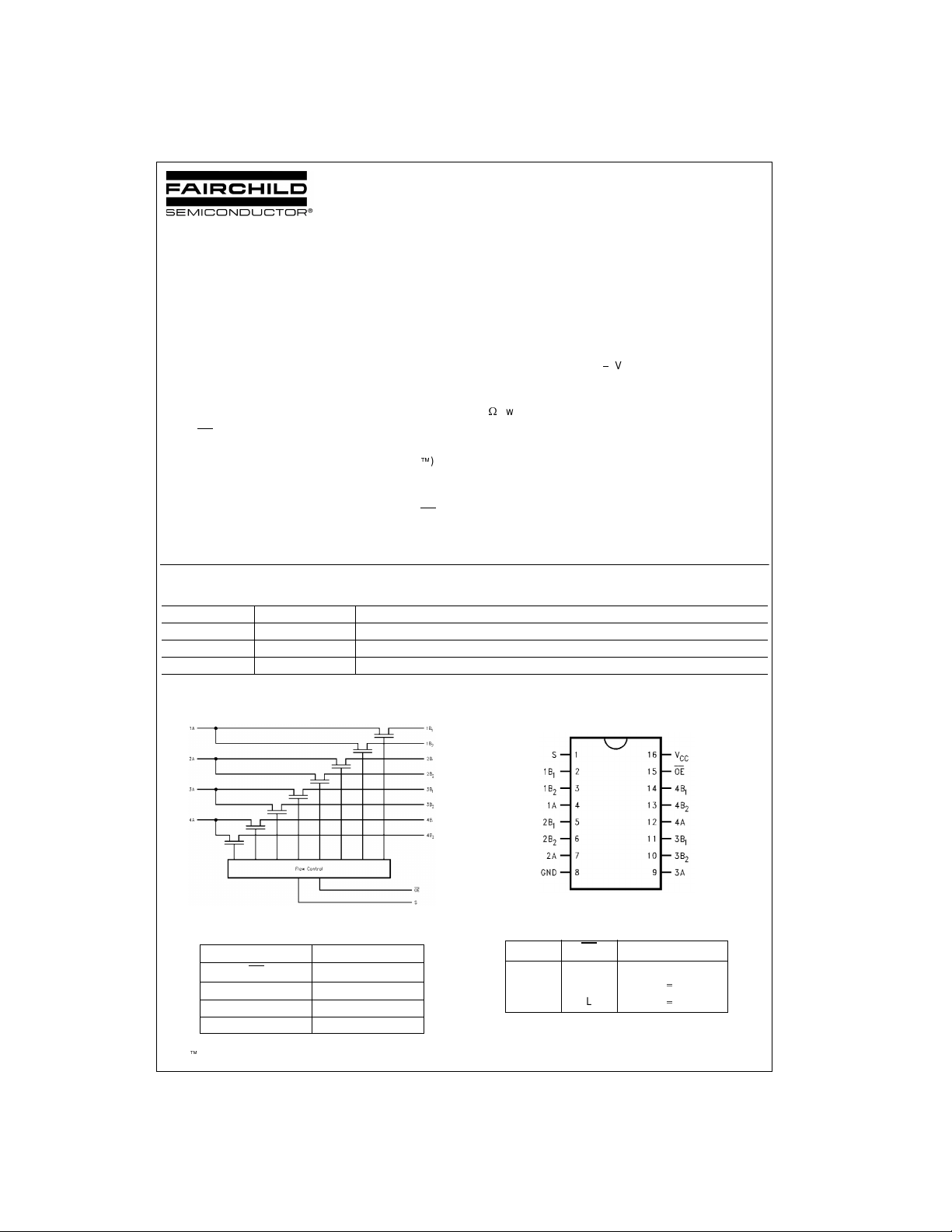
Logic Diagram
Connection Diagram
Pin Descriptions
Pin Name Description
OE
S Select Input
ABus A
B
1–B2
UHC®¥ is a registered trademark of Fairchild Semiconductor Corporation.
© 2005 Fairchild Semiconductor Corporation DS500302 www.fairchildsemi.com
Bus Switch Enable
Bus B
Truth Table
SOE Function
X H Disconnect
LL A
HL A
B
1
B
2
Page 2
Absolute Maximum Ratings(Note 1) Recommended Operating
Supply Voltage (VCC)
DC Switch Voltage (V
FSTU3257
DC Input Control Pin Voltage (V
S
DC Input Diode Current (l
DC Output (I
DC V
CC
) 128mA
OUT
/GND Current (ICC/I
Storage Temperature Range (T
) (Note 2)
) VIN 0V
IK
GND
)(Note 3)0.5V to 7.0V
IN
)
)
STG
65q
ESD
Human Body Model 5kV
0.5V to 7.0V
2.0V to 7.0V
50mA
/
100mA
C to 150 qC
Conditions
Power Supply Operating (V
Input Voltage (V
Output Voltage (V
Input Rise and Fall Time (t
Switch Control Input 0nS/V to 5nS/V
Switch I/O 0nS/V to DC
Free Air Operating Temperature (T
Note 1: The Absolute Maximum Ratings are those values beyond which
the safety of the d evice cannot be guaranteed. The device sh ould not be
operated at these limi ts. The parametric values define d in the Electrical
Characteristics tables are not gu arante ed at the abs olute max imum rat ing.
The Recommend ed Oper ating Cond itions tab les will def ine the co nditions
for actual device operation.
is the voltage obser v ed/applied at either th e A or B Ports across
Note 2: V
S
the switch.
Note 3: The input and output negative voltage ratings may be exceeded if
the input and output diode current ratings are observed.
Note 4: Unused control inputs must be held HIGH or LOW. They may not
float.
(Note 4)
) 4.0V to 5.5V
CC
)0V to 5.5V
IN
)0V to 5.5V
OUT
, tf)
r
)40 qC to 85 qC
A
DC Electrical Characteristics
V
Symbol Parameter
V
IK
V
IH
V
IL
I
I
I
OZ
R
ON
I
CC
'
I
CC
V
IKU
Note 5: Typi c al values are at VCC 5.0V and TA 25qC
Note 6: Measured by the voltage drop between A and B pins at t he indicated current th rough the switch. On re s is tan c e is determined by the lower of the
voltages on the two (A or B) pins.
Clamp Diode Voltage 4.5
HIGH Level Input Voltage 4.0–5.5 2.0 V
LOW Level Input Voltage 4.0–5.5 0.8 V
Input Leakage Current 5.5
OFF-STATE Leakage Current 5.5
Switch On Resistance 4.5 4 7
(Note 6) 4.5 4 7
Quiescent Supply Current 5.5 3
Increase in I
Voltage Undershoot 5.5
per Input 5.5 2.5 mA One input at 3.4V
CC
CC
(V)
4.5 8 15
4.0 11 20
TA 40 qC to 85 qC
Min Typ
(Note 5)
Units Conditions
Max
1.2 V IIN 18mA
r
1.0
P
r
1.0
2.0 V 0.0 mA t IIN t 50 mA
A0d VIN d5.5V
P
A0 dA, B dV
:
:
:
:
P
AVIN VCC or GND, I
CC
VIN 0V, IIN 64mA
VIN 0V, IIN 30mA
V
2.4V, IIN 15mA
IN
2.4V, IIN 15mA
V
IN
Other inputs at V
OE
5.5V
CC
0
OUT
or GND
www.fairchildsemi.com 2
Page 3

AC Electrical Characteristics
40 qC to 85qC,
T
A
C
50pF, RU RD 500
Symbol Parameter
t
t
t
Prop Delay Bus to Bus (Note 7) 0.25 0.25
PHL,tPLH
Prop Delay, Select to Bus A 7.0 30.0 35.0
, t
Output Enable Time, Select to Bus B 7.0 30.0 35.0
PZH
PZL
Output Enable Time, OE to Bus A, B 7.0 30.0 35.0 VI OPEN for t
, t
Output Disable Time, Select to Bus B 1.5 8.4 9.8
PHZ
PLZ
Output Disable Time, Output Enable Time, OE
Note 7: This parameter is guaranteed by design but is not tested. The bus switch contributes no propagation delay other than the RC delay of the typical On
resistance of the switch and the 50pF load ca pac itan c e, w hen driven by an ideal vo ltag e t he source (zero output im pedance).
to Bus A, B 1.5 8.8 9.8 VI OPEN for t
L
4.5 – 5.5V VCC 4.0V
V
CC
Min Max Min Max
:
Units Conditions
ns VI OPEN
ns
ns
VI 7V for t
VI 7V for t
PZL
PZH
PLZ
PHZ
Capacitance (Note 8)
Symbol Parameter Typ Max Units Conditions
C
IN
C
I/O
C
ON State Input/Output Capacitance ON State (A or B Port) 14 pF VCC 5.0V Switch ON
I/O
Note 8: TA 25qC, f 1 MHz, Capacitance is cha r ac t erized but not tested.
Control Pin Input Capacitance 3 pF VCC 5.0V
A Port
Input/Output Capacitance
B Port 5.5 pF
7.5 pF
VCC, OE 5.0V
Undershoot Characteristic (Note 9)
Symbol Parameter Min Typ Max Units Conditions
V
OUTU
Note 9: This is intended to characterize the device’s protective capabilities by maintaining output signal integrity during an input transient voltage undershoot
event.
Output Voltage During Undershoot 2.5 VOH 0.3 V Fig ure 1
Figure
No.
Figures
2, 3
Figures
2, 3
Figures
2, 3
FSTU3257
FIGURE 1.
Device Test Conditions Transient
Parameter Value Units
V
IN
R1 - R
V
TRI
V
CC
2
See Waveform V
100K
11.0 V
5.5 V
:
Input Voltage (V
3 www.fairchildsemi.com
) Waveform
IN
Page 4

AC Loading and Waveforms
FSTU3257
Note: Input driven by 50: source terminated in 50
Note: CL includes load and stray capacitance
Note: Input PRR
1.0 MHz, tW 500 ns
:
FIGURE 2. AC Test Circuit
FIGURE 3. AC Waveforms
www.fairchildsemi.com 4
Page 5

Physical Dimensions inches (millimeters) unless otherwise noted
FSTU3257
16-Lead Small Outline Integrated Circuit (SOIC), JEDEC MS-012, 0.150" Narrow
16-Lead Quarter Size Outline Package (QSOP), JEDEC MO-137, 0.150" Wide
Package Number M16A
Package Number MQA16
5 www.fairchildsemi.com
Page 6

Physical Dimensions inches (millimeters) unless otherwise noted (Continued)
16-Lead Thin Shrink Small Outline Package (TSSOP), JEDEC MO-153, 4.4mm Wide
Package Number MTC16
Technology Description
The Fairchild Switch family derives from and embodies Fairchild ’s proven switch tec hnology used fo r several years in its
74LVX3L384 (FST3384) bus switch product.
Fairchild does not assume any responsibility for use of an y circuitry described, no circuit patent licenses are imp lied and
Fairchild reserves the right at any time without notice to change said circuitry and specifications.
FSTU3257 Quad 2:1 Multiplexer/Demultiplexer Bus Switch with 2V Undershoot Protection
LIFE SUPPORT POLICY
FAIRCHILD’S PRODUCTS ARE NOT AUTHORIZED FOR USE AS CRITICAL COMPONENTS IN LIFE SUPPORT
DEVICES OR SYSTEMS WITHOUT THE EXPRESS WRITTEN APPROVAL OF THE PRESIDENT OF FAIRCHILD
SEMICONDUCTOR CORPORATION. As used herein:
1. Life support devices or systems are devices or syste ms
which, (a) are intended for surgical implant into the
body, or (b) support or sustain life, and (c) whose failure
to perform when properly used in accordance with
instructions for use provided in the labeling, can be reasonably expected to result in a significant inju ry to the
user.
www.fairchildsemi.com 6
2. A critical component in any componen t of a life support
device or system whose failu re to perform can be reasonably expected to cause the failure of the lif e su pp ort
device or system, or to affect its safety or effectiveness.
www.fairchildsemi.com
 Loading...