

Page 1
© 2000 Fairchild Semiconductor Corporation DS500258 www.fairchildsemi.com
June 1999
Revised March 2000
FSTU32160A 16-Bit to 32-Bit Multiplexer/Demultiplexer Bus Switch with −2V Undershoot Protection
FSTU32160A
16-Bit to 32-Bit Multiplexer/Demultiplexer Bus Switch
with −2V Undershoot Protection
General Description
The Fairchild Switch FSTU32160A is a 16-bit to 32-bit
high-speed CMOS TTL-compatible multiplexer/demultiplexer bus switch. The low on resistance of the switch
allows inputs to be c onnected to outputs without adding
propagation delay or generatin g additiona l ground boun ce
noise.
The device can be used in app lications where two buses
need to be addressed simultaneously. The FSTU32160A is
designed so that the A Port de multiplexe s into B
1
or B2 or
both. The A and B Ports are “under shoot hardened” with
UHC protection to support an e xtended range to 2.0V
below ground. Fairchi ld’s integ rated U nde rshoot Hard ened
Circuit, UHC senses undershoot at the I/O’s, and responds
by preventing voltage differentials from developing and
turning on the switch.
Two select (SEL
1
, SEL2) inputs provide switch enabl e co n-
trol. When SEL
1
, SEL2 are HIGH, the devic e precharges
the B Port to a selectable bias voltage (Bias V) to minimize
live insertion noise.
Features
■ Undershoot hardened to −2V (A and B Ports).
■ 4Ω switch connection between two ports.
■ Minimal propagation delay through the switch.
■ Low l
CC
.
■ Zero bounce in flow-through mode.
■ Control inputs compatible with TTL level.
■ See Applications Note AN-5008 for details
Ordering Code:
Devices also availab le in Tape and Reel. Specify by appending th e s uffix let t er “X” to the ordering code.
UHC is a trademark of Fairc hild Semiconductor C orporation.
Order Number Package Number Package Description
FSTU32160A MTD MTD56 56-Lead Thin Shrink Small Outline Package (TSSOP), JEDEC MO-153, 6.1mm Wide
Page 2
www.fairchildsemi.com 2
FSTU32160A
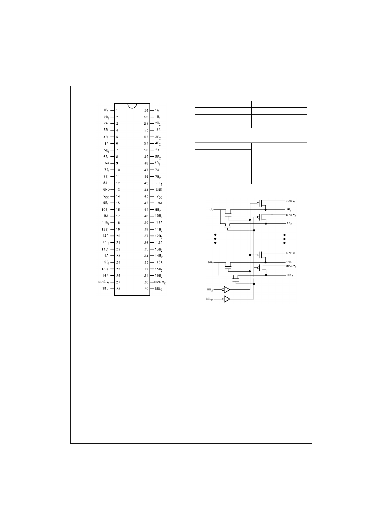
Connection Diagram Pin Descriptions
Tr uth Table
Logic Diagram
Pin Name Description
SEL
1
, SEL
2
Select Inputs
ABus A
B
1
, B
2
Bus B
Inputs
Function
SEL
1
SEL
2
LH x A = x B
1
HL x A = x B
2
LLx A = x B1 and x B
2
H H x B1, x B2 = BiasV
Page 3

3 www.fairchildsemi.com
FSTU32160A
Absolute Maximum Ratings(Note 1) Recommended Operating
Conditions
(Note 4)
Note 1: The “Absolute Maximum Ratings ” are those val ues beyond w hich
the safety of the device cannot be guaranteed. The device should not be
operated at these limits. The parametric values defined in the Electrical
Characteristics tables are not guaranteed at the absolute maximum rating.
The “Recommend ed O peratin g Cond itions” t able w ill defin e the condition s
for actual device operation.
Note 2: V
S
is the voltage observed/applied at either the A or B Ports across
the switch.
Note 3: The input and output negativ e voltage ra tings ma y be excee ded if
the input and output diode current ratings are observed.
Note 4: Unused control inputs m ust be held HIGH o r LOW. They m ay n ot
float.
DC Electrical Characteristics
Note 5: Typical values are at VCC = 5.0V and TA = +25°C
Note 6: Measured by t he v oltage drop between A and B pins at the indicated c urrent through the swi tch. On resistance is det ermined by the lower of the
voltages on the two (A or B) pins.
Supply Voltage (VCC) −0.5V to +7.0V
DC Switch Voltage (V
S
) (Note 2) −2.0V to +7.0V
BiasV Voltage Range −0.5V to +7.0V
DC Input Control Pin Voltage
(V
IN
) (Note 3) −0.5V to +7.0V
DC Input Diode Current (l
IK
) V
IN
< 0V −50 mA
DC Output Current (I
OUT
)128 mA
DC V
CC
/GND Current (ICC/I
GND
) +/− 100 mA
Storage Temperature Range (T
STG
) −65°C to +150 °C
Power Supply Operating (V
CC
) 4.0V to 5.5V
Precharge S upply (Bias V) 1 .5 to V
CC
Input Voltage (VIN) 0V to 5.5V
Output Voltage (V
OUT
) 0V to 5.5V
Input Rise and Fall Time (t
r
, tf)
Switch Control Input 0nS/V to 5nS/V
Switch I/O 0nS/V to DC
Free Air Operating Temperature (T
A
) −40 °C to +85 °C
Symbol Parameter
TA = −40 °C to +85 °C
Units ConditionsV
CC
Min Typ Max
(V) (Note 5)
V
IK
Clamp Diode Voltage 4.5 −1.2 V IIN = −18mA
V
IH
HIGH Level Input Voltage 4.0–5.5 2.0 V
V
IL
LOW Level Input Voltage 4.0–5.5 0.8 V
I
I
Input Leakage Current 5.5 ±1.0 µA0 ≤ VIN ≤ 5.5V
010µAVIN = 5.5V
I
O
Output Current 4.5 0.25 mA BiasV = 2.4V
BX = 0
I
OZH
, I
OZL
OFF-STATE Leakage Current 5.5 ±1.0 µA0 ≤ A ≤ VCC, V
BiasV1 = BiasV2 = 5.5V
I
OZH
, I
OZL
OFF-STATE Leakage Current 5.5 ±1.0 µA0 ≤ B ≤ VCC, V
BiasV1 = BiasV2 = Floating
R
ON
Switch On Resistance 4.5 4 7 Ω VIN = 0V, IIN = 64 mA
(Note 6) 4.5 4 7 Ω VIN = 0V, IIN = 30 mA
4.5 8 14 Ω VIN = 2.4V, IIN = 15 mA
4.0 11 20 Ω VIN = 2.4V, IIN = 15 mA
I
CC
Quiescent Supply Current 5.5 3 µAVIN = VCC or GND, I
OUT
= 0
∆ I
CC
Increase in I
CC
per Input 5.5 2.5 mA One input at 3.4V
Other inputs at VCC or GND
I
BIAS
Bias Pin Leakage Current 5.5 ±1.0 µASEL1, SEL2 = 0V
BX = 0V, BiasVX = 5.5V
V
IKU
Voltage Undershoot 5.5 −2.0 V 0.0 mA ≥ IIN ≥ −50 mA
SEL1, SEL2 = 5.5V
Page 4

www.fairchildsemi.com 4
FSTU32160A
AC Electrical Characteristics
Note 7: This parameter is guaranteed by design but is not tested. The bus switch contributes no propagation delay other than the RC delay of the typical On
resistance of the sw it c h and the 50pF load capa c it ance, when driven by an ideal voltage source (z ero output impedance).
Capacitance (Note 8)
Note 8: TA = +25°C, f = 1 Mhz, Capacitance is ch aracterized but not teste d.
Undershoot Characteristic (Note 9)
Note 9: This is intended to characterize the device’s protective capabilities by maintaining output signal integrity during an input transient voltage und ershoot
event.
FIGURE 1.
Device Test Conditions Tr ansient
Input Voltage (V
IN
) Waveform
Symbol Parameter
TA = −40 °C to +85 °C,
CL = 50 pF, RU= RD = 500Ω
Units Conditions Figure No.
VCC = 4.5 − 5.5V VCC = 4.0V
Min Max Min Max
t
PHL
, t
PLH
A or B, to B or A (Note 7) 0.25 0.25 ns VI = OPEN Figure 2
Figure 3
t
PZH
Output Enable Time,
0.5 4.0 4.5 ns
VI = OPEN for t
PZH
Figure 2
Figure 3
SEL to A, B BiasV = GND
t
PZL
Output Enable Time,
1.0 4.8 5.5 ns
VI = 7V for t
PZL
Figure 2
Figure 3
SEL to A, B BiasV = 3V
t
PHZ
Output Disable Time,
1.0 5.9 6.9 ns
VI = Open for t
PHZ
Figure 2
Figure 3
SEL to A, B BiasV = GND
t
PLZ
Output Disable Time,
1.0 7.4 7.0 ns
VI = 7V for t
PLZ
Figure 2
Figure 3
SEL to A, B BiasV = 3V
Symbol Parameter Typ Max Units Conditions
C
IN
Control pin Input Capacitance 4 pF VCC = 5.0V
C
I/O OFF
Input/Output Capacitance “OFF State” 8 pF VCC = 5.0V, Switch OFF
Symbol Parameter Min Typ Max Units Conditions
V
OUTU
Output Voltage During Undershoot 2.5 VOH − 0.3 V Figure 1
Parameter Value Units
V
IN
See Waveform V
R1 - R
2
100K Ω
V
TRI
11.0 V
V
CC
5.5 V
Page 5

5 www.fairchildsemi.com
FSTU32160A
AC Loading and Waveforms
Note: Input driven by 50 Ω source terminated in 50Ω
Note: C
L
includes load and stray capacitance, CL = 50 pF
Note: Input PRR = 1.0 MHz, t
W
= 500 ns
FIGURE 2. AC Test Circuit
FIGURE 3. AC Waveforms
Page 6

www.fairchildsemi.com 6
FSTU32160A 16-Bit to 32-Bit Multiplexer/Demultiplexer Bus Switch with −2V Undershoot Protection
Physical Dimensions inches (millimeters) unless otherwise noted
56-Lead Thin Shrink Small Outline Package (TSSOP), JEDEC MO-153, 6.1mm Wide
Package Number MTD56
Technology Description
The Fairchild Switch family derives from and embodies Fairchild’s proven switch technology us ed for several years in its
74LVX3L384 (FST3384) bus switch product.
Fairchild does not assume any responsibility for use of any circuitry described, no circuit pate nt licenses are implied and
Fairchild reserves the right at any time without notice to change said circuitry and specifications.
LIFE SUPPORT POLICY
FAIRCHILD’S PRODUCTS ARE NOT AUTHORIZED FOR USE AS CRITICAL COMPONENTS IN LIFE SUPPORT
DEVICES OR SYSTEMS WITHOUT THE EXPRESS WRITTEN APPROVAL OF THE PRESIDENT OF FAIRCHILD
SEMICONDUCTOR CORPORATION. As used herein:
1. Life support devices or systems are devices or syste ms
which, (a) are intended for surgical implant into the
body, or (b) support or sustain life, and (c) whose failure
to perform when properly used in accordance with
instructions for use provided in the labeling, can be reasonably expected to result in a significant inju ry to the
user.
2. A critical component i n any compon ent of a lif e support
device or system whose failu re to perform can be reasonably expected to ca use the fa i lure of the life su pp ort
device or system, or to affect its safety or effectiveness.
www.fairchildsemi.com
 Loading...