

Page 1
FSTU16211
Preliminary
FSTU16211 24-Bit Bus Switch with
May 2001
Revised May 2001
24-Bit Bus Switch with
−2V Undershoot Protection
(Preliminary)
General Description
The Fairchild Sw itch FSTU162 11 provides 24-bits of hi ghspeed CMOS TTL-compatible bus switching. The low On
Resistance of the switch allows inputs to be connected to
outputs without adding propagation delay or generating
additional ground bounce noise.
The device is organ ized as a 12-bit or 24-bit b us switch.
When OE
nected to Port 1B. When OE
to Port 2B. The A and B Ports are protected against under-
shoot to support an extend ed rang e to 2.0V be low gr ound.
Fairchild’s integrated Undershoot Hardened Circuit
(UHC
preventing voltage differentials from developing and turning the switch on.
is LOW, the switch is ON and Port 1A is con-
1
) senses undershoot at the I/O and responds by
is LOW, Port 2A is connected
2
Ordering Code:
Order Number Package Number Package Description
FSTU16211MTD MTD56 56-Lead Thin Shrink Small Outline Package (TSSOP), JEDEC MO-153, 6.1mm Wide
Devices also availab l e in Tape and Reel. Specify by appending th e s uffix let t er “X” to the ordering code.
Features
■ Undershoot hardened to −2V (A and B Ports)
■ Slower output enable times to prevent signal disruption
■ 4
Ω switch connection between two ports
■ Minimal propagation delay through the switch
■ Low l
CC
■ Zero bounce in flow-through mode
■ Control inputs compatible with TTL level
■ See Applications Note AN-5008 for details
−
2V Undershoot Protection (Preliminary)
UHC is a trademark of Fairchild Semiconductor Corporation.
© 2001 Fairchild Semiconductor Corporation DS500389 www.fairchildsemi.com
Page 2
Preliminary
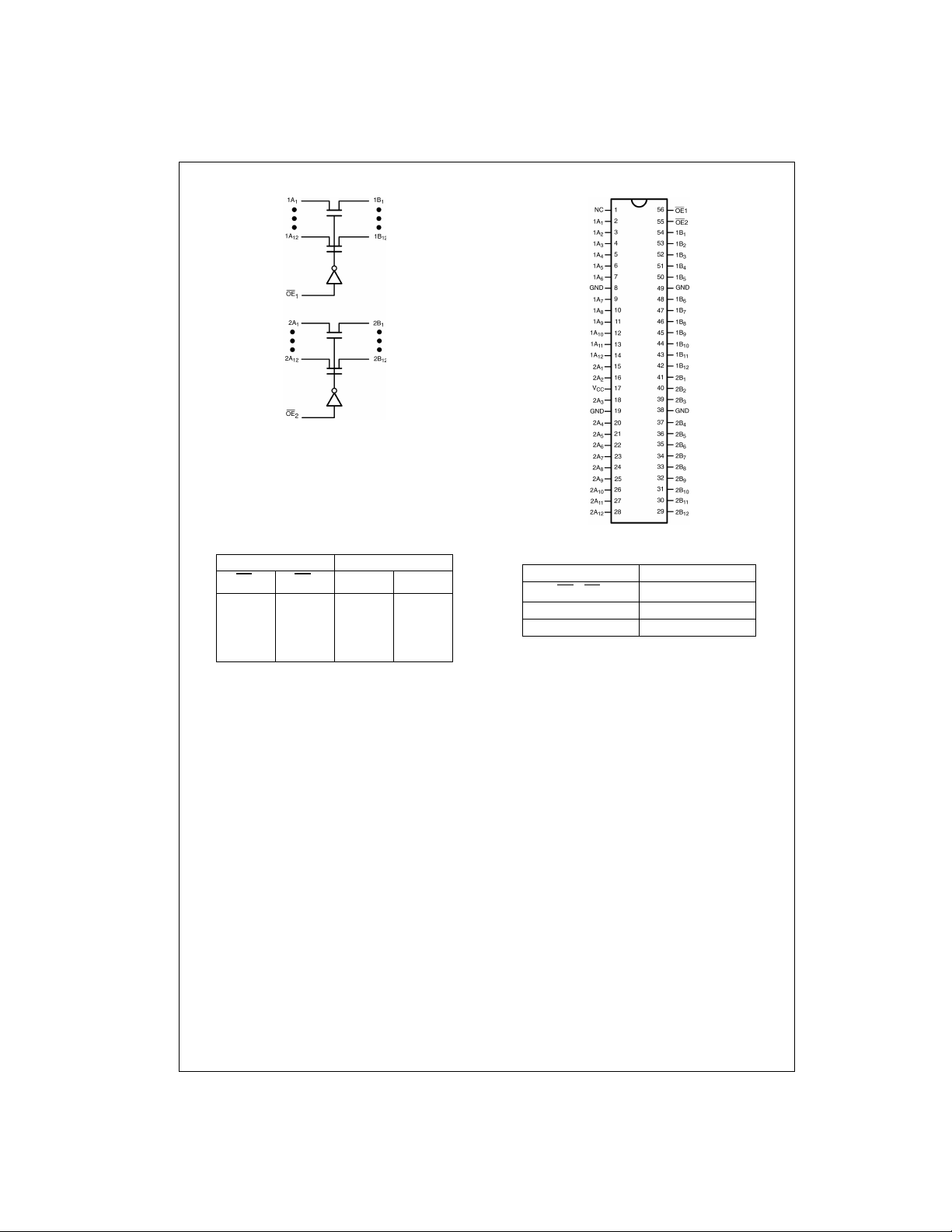
Logic Diagram
FSTU16211
Truth Table
OE
1
LL1A
LH1A
HLZ2A
HHZZ
Inputs Inputs/Outputs
OE
1A, 1B 2A, 2B
2
= 1B 2A = 2B
= 1B Z
= 2B
Connection Diagram
Pin Descriptions
Pin Name Description
OE
, OE
1
2
1A, 2A Bus A
1B, 2B Bus B
Bus Switch Enables
www.fairchildsemi.com 2
Page 3

Preliminary
Absolute Maximum Ratings(Note 1) Recommended Operating
Supply Voltage (VCC) −0.5V to +7.0V
DC Switch Voltage (V
) (Note 2) −0.5V to +7.0V
S
DC Input Control
Pin Voltage (V
DC Input Diode Current (l
DC Output Current (I
/GND Current (ICC/I
DC V
CC
Storage Temperature Range (T
) (Note 3) −0.5V to +7.0V
IN
) V
< 0V −50 mA
IK
IN
) 128 mA
OUT
) +/− 100 mA
GND
) −65°C to +150 °C
STG
Conditions
Power Supply Operating (V
Input Voltage (V
Output Voltage (V
Input Rise and Fall Time (t
Switch Control Input 0 ns/V to 5 ns/V
Switch I/O 0 ns/V to DC
Free Air Operating Temperature (T
Note 1: The “Absolute Maximum Ratings” are those value s beyond which
the safety of the d evice cannot b e guaranteed . The device sh ould not be
operated at these limit s. The parametric values defi ned in the Electrical
Characteristics tables are not guaranteed at the absolute maximum rating.
The “Recomm ended O peratin g Cond itions ” table will defin e the condition s
for actual device operation.
is the volt age observed/applied a t either the A or B Ports across
Note 2: V
S
the switch.
Note 3: The input and output negative voltage ratings may be exceeded if
the input and ou t put diode current ratings ar e observed.
Note 4: Unused control inputs must be held HIGH or LOW. They may not
float.
(Note 4)
CC)
) 0V to 5.5V
IN
) 0V to 5.5V
OUT
, tf)
r
)-40 °C to +85 °C
A
4.0V to 5.5V
DC Electrical Characteristics
V
Symbol Parameter
V
IK
V
IH
V
IL
I
I
I
OZ
R
ON
I
CC
∆ I
CC
V
IKU
Note 5: Typical values are at VCC = 5.0V and TA = +25°C
Note 6: Measured by the voltage drop between A and B pins at the indicated c urrent through the switch. On Resistanc e is determined by the lower of the
voltages on the two (A or B) pins.
Clamp Diode Voltage 4.5 −1.2 V IIN = −18 mA
HIGH Level Input Voltage 4.0–5.5 2.0 V
LOW Level Input Voltage 4.0–5.5 0.8 V
Input Leakage Current 5.5 ±1.0 µA0 ≤ VIN ≤ 5.5V
OFF-STATE Leakage Current 5.5 ±1.0 µA0 ≤ A, B ≤ V
Switch On Resistance 4.5 4 7 Ω VIN = 0V, IIN = 64 mA
(Note 6) 4.5 4 7 Ω V
Quiescent Supply Current 5.5 3 µAVIN = VCC or GND, I
Increase in I
Voltage Undershoot 5.5 −2.0 V 0.0 mA ≥ IIN ≥ −50 mA
per Input 5.5 2.5 mA One Input at 3.4V
CC
CC
(V)
010µAV
4.5 8 12 Ω V
4.0 11 20 Ω VIN = 2.4V, IIN = 15 mA
TA = −40 °C to +85 °C
Min Typ
(Note 5)
Units Conditions
Max
= 5.5V
IN
CC
= 0V, IIN = 30 mA
IN
= 2.4V, IIN = 15 mA
IN
OUT
Other Inputs at VCC or GND
= 5.5v
OE
1,2
FSTU16211
= 0
3 www.fairchildsemi.com
Page 4

Preliminary
AC Electrical Characteristics
= −40 °C to +85 °C,
T
A
C
= 50pF, RU = RD = 500Ω
Symbol Parameter
FSTU16211
t
, t
PHL
t
PZH
t
PHZ
Note 7: This parameter is guaranteed by design but is not tested. The bus switch contributes no propagation delay other than the RC delay of the typical On
Resistance of the s witch and the 50pF load capacitance, wh en driven by an ideal volt age source (zero output impedance).
Propagation Delay Bus to Bus
PLH
(Note 7)
, t
Output Enable Time 7.0 30.0 35.0 ns VI = 7V for t
PZL
, t
Output Disable Time 1.5 7.0 7.2 ns VI = 7V for t
PLZ
L
= 4.5 – 5.5V VCC = 4.0V
V
CC
Min Max Min Max
0.25 0.25 ns VI = OPEN F igures 2,
Units Conditions
= OPEN for t
I
PZL
PZH
PLZ
PHZ
VI = OPEN for t
V
Capacitance (Note 8)
Symbol Parameter Typ Max Units Conditions
C
IN
C
I/O
Note 8: TA = +25°C, f = 1 MHz, Capacitance is characterized but not tested.
Control Pin Input Capacitance 3 pF VCC = 5.0V
Input/Output Capacitance 6 pF VCC, OE = 5.0V
Undershoot Characteristic
Symbol Parameter Min Typ Max Units Conditions
V
OUTU
Note 9: This test is intended to charac t erize the device’s protect iv e c apabilities by maintaining output signal integrity during an input tran s ient voltage under-
shoot event.
Output Voltage During Undershoot 2.5 VOH − 0.3 V
Figure
Number
3
Figures 2,
3
Figures 2,
3
FIGURE 1.
Device Test Conditions Transient
Parameter Value Units
V
R1 = R
V
TRI
V
CC
IN
see Waveform V
2
100K Ω
11.0 V
5.5 V
www.fairchildsemi.com 4
Input Voltage (V
) Waveform
IN
Page 5

AC Loading and Waveforms
Note: Input driven by 50 Ω source terminated in 50 Ω
includes load and stray capacitance
Note: C
L
Note: Input PRR = 1.0 MHz, t
= 500 ns
W
Preliminary
FSTU16211
FIGURE 2. AC Test Circuit
FIGURE 3. AC Waveforms
5 www.fairchildsemi.com
Page 6
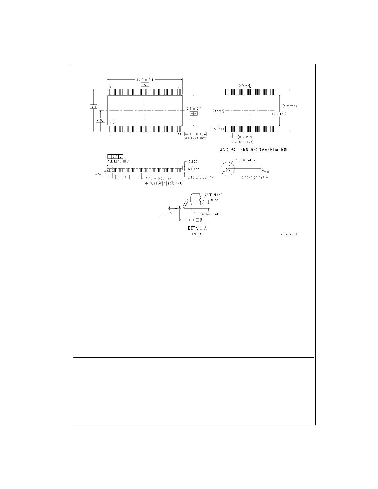
Physical Dimensions inches (millimeters) unless otherwise noted
2V Undershoot Protection (Preliminary)
−
Preliminary
56-Lead Thin Shrink Small Outline Package (TSSOP), JEDEC MO-153, 6.1mm Wide
Package Number MTD56
Technology Description
The Fairchild Switch family derives from and embodies Fairchild’s proven s witch technol ogy used for several years i n its
74LVX3L384 (FST3384) bus switch product.
FSTU16211 24-Bi t Bus Switch with
Fairchild does not assume any responsibility for use of any circuitr y described, no circuit patent licenses are implied a nd
Fairchild reserves the right at any time without notice to change said circuitry and specifications.
LIFE SUPPORT POLICY
FAIRCHILD’S PRODUCTS ARE NOT AUTHORIZED FOR USE AS CRITICAL COMPONENTS IN LIFE SUPPORT
DEVICES OR SYSTEMS WITHOUT THE EXPRESS WRITTEN APPROVAL OF THE PRESIDENT OF FAIRCHILD
SEMICONDUCTOR CORPORATION. As used herein:
1. Life support devices or systems are device s or syste ms
which, (a) are intended for surgical implant into the
body, or (b) support or sustain life, and (c) whose failure
to perform when properly used in accordance with
instructions for use provided in the labeling, can be reasonably expected to result in a significant inju ry to the
user.
2. A critical component in any compon ent of a l ife supp ort
device or system whose failu re to perform can be reasonably expected to cause the failure of the li fe su pp ort
device or system, or to affect its safety or effectiveness.
www.fairchildsemi.com
www.fairchildsemi.com 6
 Loading...