

Page 1
February 2001
Revised February 2001
FSTD3306
2-Bit Low Power Bus Switch with Level Shifting
FSTD3306 2-Bit Low Power Bus Switch with Level Shifting
General Description
The FSTD3306 is a 2-bit ult ra high-sp eed CMOS FET bus
switch with enhanced level sh ifting circuitry and w ith TTLcompatible active LOW c ontrol inputs. The low on resistance of the switch allows inputs to be connect ed to outputs with minimal propagation delay and without
generating addition al ground bounce nois e. The device is
organized as a 2-bit swi tch with independent bus enabl e
(BE
) controls. When BE is LOW, the switch is ON and Port
A is connected to Port B. When BE
OPEN and a high-impedance sta te exist s between the two
ports. Reduced voltag e drive to the gat e of the FET switch
permits nominal level shifting of 5V to 3V through the
switch. Control inputs tolerate voltages up to 5.5V independent of V
.
CC
is HIGH, the switch is
Features
■ Typical 3Ω switch resistance at 5.0V VCC, VIN = 0V
■ Level shift facilitates 5V to 3.3V interfacing
■ Minimal propagation delay through the switch
■ Power down high impedance input/output
■ Zero bounce in flow t h rough mode
■ TTL compatible active LOW control inputs
■ Control inputs are overvoltage tolerant
Ordering Code:
Order Number Package Number Package Description
FSTD3306MTC MTC08 8-Lead Thin Shrink Small Outline Package (TS SOP), JEDEC MO-153, 4.4mm Wide
Devices also availab le in Tape and Reel. Specify by appending the suffix letter “X” to the o rdering code.
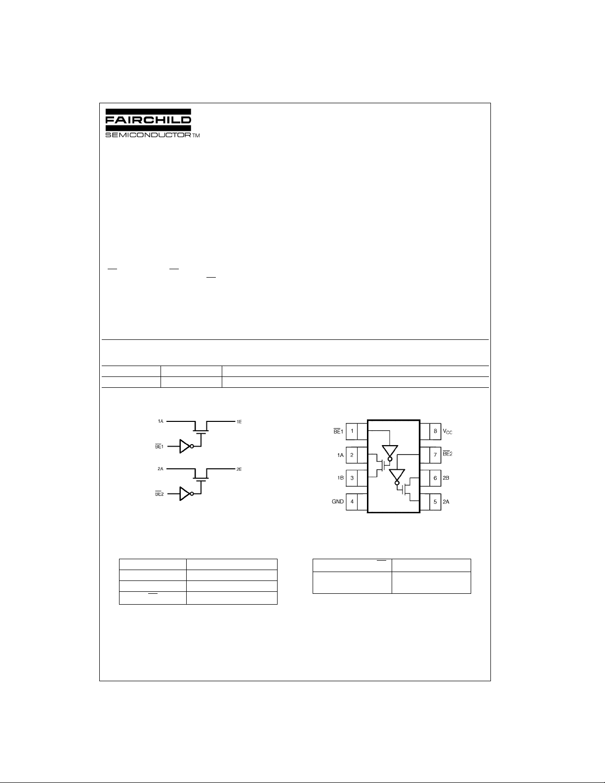
Logic Diagram Connection Diagram
(Top View)
Pin Descriptions Function Table
Pin Name Description
A Bus A Switch I/O
B Bus B Switch I/O
BE
© 2001 Fairchild Semiconductor Corporation DS500480 www.fairchildsemi.com
Bus Enable Input
Bus Enable Input (BE) Function
L B Connected to A
H = HIGH Logic Level
L = LOW Logic Level
H Disconnected
Page 2
Absolute Maximum Ratings(Note 1) Recommended Operating
Supply Voltage (VCC) −0.5V to +7.0V
DC Switch Voltage (V
FSTD3306
DC Output Voltage (V
) −0.5V to +7.0V
S
) (Note 2) −0.5V to +7.0V
IN
DC Input Diode Current
) VIN < 0V −50 mA
(I
IK
DC Output (I
DC V
CC
(I
CC/IGND
Storage Temperature Range (T
) Sink Current 128 mA
OUT
or Ground Current
) ±100 mA
) −65°C to +150°C
STG
Junction Temperature
under Bias (T
Junction Lead Temperature (T
) +150°C
J
)
L
(Soldering, 10 Seconds)
Power Dissipation (P
) @ +85°C250 mW
D
+260°C
Conditions
Supply Operating (V
Control Input Voltage (V
Switch Input Voltage (V
Switch Output Voltage (V
Operating Temperature (T
Input Rise and Fall Time (t
Control Input 0 ns/V to 5 ns
Switch I/O 0 ns/V to DC
Thermal Resistance (
Note 1: The “Absolute Maximum Ratings” are those values bey ond which
the safety of the d evice cannot be guaranteed. The device sh ould not be
operated at these limit s. The parametric values defin ed in the Electrical
Characteristics tables are not guaranteed at the absolute maximum ratings.
The “Recomme nded O peratin g Cond itions ” table will defin e the condition s
for actual device operation.
Note 2: The input and output ne gative vo ltage ra tings may be excee ded if
the input and output diode current ratings are observed.
Note 3: Unused logic inputs must be held HIGH or LOW. They may not
float.
(Note 3)
) 4.5V to 5.5V
CC
) 0V to 5.5V
IN
) 0V to 5.5V
IN
) 0V to 5.5V
OUT
) −40°C to +85°C
A
, tf)
r
θ
)250°C/W
JA
DC Electrical Characteristics
V
Symbol Parameter
V
IK
V
IH
V
IL
V
OH
I
IN
I
OFF
R
ON
I
CC
∆ I
Note 4: Measured by the volta ge drop between A an d B pins at the indicated c urrent through the switch. On resistance is determined by the lower of the
voltages on the two (A or B) pins.
Note 5: Per TTL driven input (V
Clamp Diode Voltage 4.5 −1.2 V IIN = −18 mA
HIGH Level Input Voltage 4.5–5.5 2.0 V
LOW Level Input Voltage 4.5–5.5 0.8 V
HIGH Level Output Voltage 4.5–5.5 see Figure 3 V VIN = V
Input Leakage Current 5.5 ±1.0 µA0 ≤ VIN ≤ 5.5V
Power OFF Leakage Current 5.5 ±1.0 µA0 ≤ A, B ≤ V
Switch On Resistance 4.5 3 7
(Note 4) 4.5 3 7 V
Quiescent Supply Current 5.5 VIN = VCC or GND, I
Increase in ICC per Input
CC
(Note 5) Input Only, Other BE = V
= 3.4V, control input only). A and B pins do not contribute to ICC.
IN
CC
(V) Min Typ Max
4.5 15 50 VIN = 2.4V, IIN = 15 mA
5.5 1 2.5 mA
TA = −40°C to +85°C
1.1 1.5 mA BE
10 µABE1 = BE2 = V
Units Conditions
CC
VIN = 0V, IIN = 64 mA
Ω
VIN = 3.4V, IO = 0, one Control
CC
= 0V, IIN = 30 mA
IN
= BE2 = GND
1
= 0
OUT
CC
CC
www.fairchildsemi.com 2
Page 3

AC Electrical Characteristics
TA = −40°C to +85°C,
Symbol Parameter
V
CL = 50 pF, RU = RD = 500Ω
CC
Units Conditions
(V) Min Typ Max
t
, Prop Delay Bus to Bus 4.5–5.5 0.25 ns VI = OPEN Figures
PHL
t
t
t
t
t
(Note 6)
PLH
, Output Enable Time 4.5–5.5 1.0 3.5 5.8 ns VI = 7V for t
PZL
PZH
, Output Disable Time 4.5–5.5 0.8 3.5 4.8 ns VI = 7V for t
PLZ
PHZ
Note 6: This parameter is guarant eed. The bu s switch contrib utes no pro pagatio n delay ot her tha n the RC de lay of the ty pical On re sistance of the switch
and the 50 pF load capac it ance, when driven by an ideal voltage sourc e (z ero output impedanc e). The specified limit i s ca lc ulated on this basis.
VI = 0V for t
VI = 0V for t
PZL
PZH
PLZ
PHZ
Figure
Number
Figures
Figures
Capacitance
Symbol Parameter Typ Max Units Conditions
C
IN
C
(OFF) Port OFF Capacitance 6 pF VCC = 5.0V = BE
I/O
C
(ON) Port ON Capacitance 12 pF VCC = 5.0V, BE = 0V
I/O
Control Pin Input Capacitance 2.5 pF VCC = 0V
AC Loading and Waveforms
Input driven by 50Ω source terminated in 50Ω
includes load and stray capacitance
C
L
Input PRR = 1.0 MHz; t
= 500 ns
W
FSTD3306
1, 2
1, 2
1, 2
FIGURE 1. AC Test Circuit
FIGURE 2. AC Waveforms
3 www.fairchildsemi.com
Page 4

DC Characteristics
FSTD3306
FIGURE 3. Typical High Level Output Voltage vs. Supply Voltage
www.fairchildsemi.com 4
Page 5

Physical Dimensions inches (millimeters) unless otherwise noted
FSTD3306 2-Bit Low Power Bus Switch with Level Shifting
8-Lead Thin Shrink Small Outline Package (TSSOP), JEDEC MO-153, 4.4mm Wide
Fairchild does not assume any responsibility for use of any circuitry described , no circuit patent licenses are implied and
Fairchild reserves the right at any time without notice to change said circuitry and specifications.
LIFE SUPPORT POLICY
FAIRCHILD’S PRODUCTS ARE NOT AUTHORIZED FOR USE AS CRITICAL COMPONENTS IN LIFE SUPPORT
DEVICES OR SYSTEMS WITHOUT THE EXPRESS WRITTEN APPROVAL OF THE PRESIDENT OF FAIRCHILD
SEMICONDUCTOR CORPORATION. As used herein:
1. Life support devices or systems are dev ic es or syste ms
which, (a) are intended for surgical implant into the
body, or (b) support or sustain life, and (c) whose failure
to perform when properly used in accordance with
instructions for use provide d in the l abe ling, can be reasonably expected to result in a significant injury to the
user.
Package Number MTC08
2. A critical compo nent in any com ponen t of a life s upp ort
device or system whose failure to perform can be reasonably expected to cause the failure of the life support
device or system, or to affect its safety or effectiveness.
www.fairchildsemi.com
5 www.fairchildsemi.com
 Loading...