

Page 1

FD
S
89
C
ua
&
C
a
e
o
e
e
c
OS
November 2005
FDS4897C
Dual N & P-Channel PowerTrench® MOSFET
General Description
These dual N- and P-Channel enhancement mode
power field effect transistors are produced using
Fairchild Semiconductor’s advanced PowerTrench
process that has been especially tailored to minimize
on-state resistance and yet maintain superior switching
performance.
Application
• Inverter
• Power Supplies
D2
D
D2
D
D1
D
D1
D
SO-8
Pin 1
SO-8
S1
G2
S2
G
G1
S
S
S
Features
• Q1: N-Channel
6.2A, 40V R
R
• Q2: P-Channel
–4.4A, –40V R
R
• High power handling capability in a widely used
surface mount package
• RoHS compliant
5
6
7
8
= 29mΩ @ VGS = 10V
DS(on)
= 36mΩ @ VGS = 4.5V
DS(on)
= 46mΩ @ VGS = –10V
DS(on)
= 63mΩ @ VGS = –4.5V
DS(on)
Q2
Q1
4
3
2
1
4
7
D
l N
Ph
nn
l P
w
rTr
n
h
®
M
FET
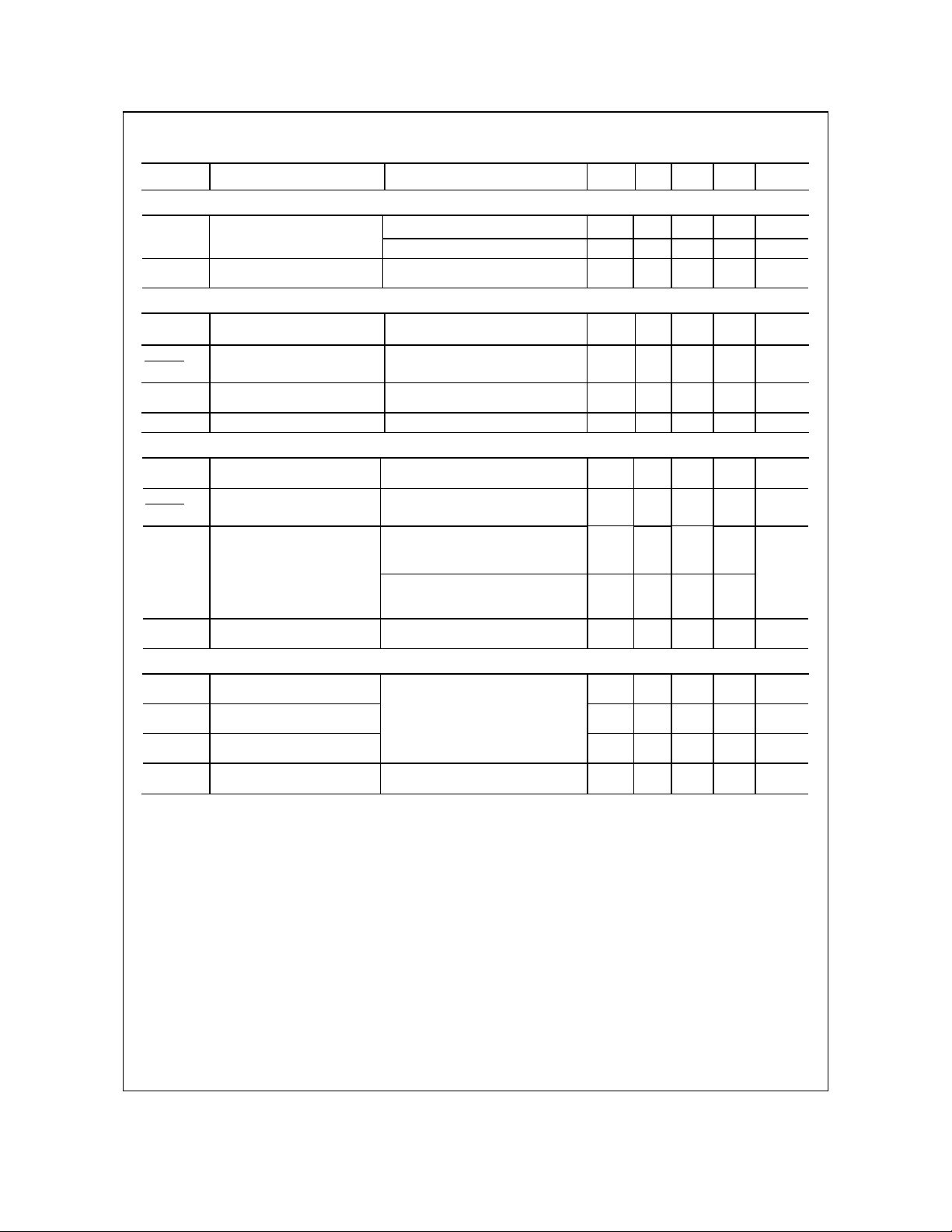
Absolute Maximum Ratings T
= 25°C unless otherwise noted
A
Symbol Parameter Q1 Q2 Units
V
Drain-Source Voltage 40 40 V
DSS
V
Gate-Source Voltage
GSS
ID Drain Current - Continuous (Note 1a) 6.2 –4.4 A
- Pulsed 20 –20
PD Power Dissipation for Dual Operation 2 W
Power Dissipation for Single Operation (Note 1a) 1.6
TJ, T
STG
Operating and Storage Junction Temperature Range –55 to +150
(Note 1b)
(Note 1c)
±20 ±20
1
0.9
V
°C
Thermal Characteristics
R
θJA
R
θJC
Thermal Resistance, Junction-to-Ambient
Thermal Resistance, Junction-to-Case
(Note 1a) 78
(Note 1) 40
°C/W
°C/W
Package Marking and Ordering Information
Device Marking Device Reel Size Tape width Quantity
FDS4897C FDS4897C 13” 12mm 2500 units
©2005 Fairchild Semiconductor Corporation
FDS4897C Rev C(W)
www.fairchildsemi.com
Page 2
S
89
C
ua
&
C
a
e
o
e
e
c
OS
FD
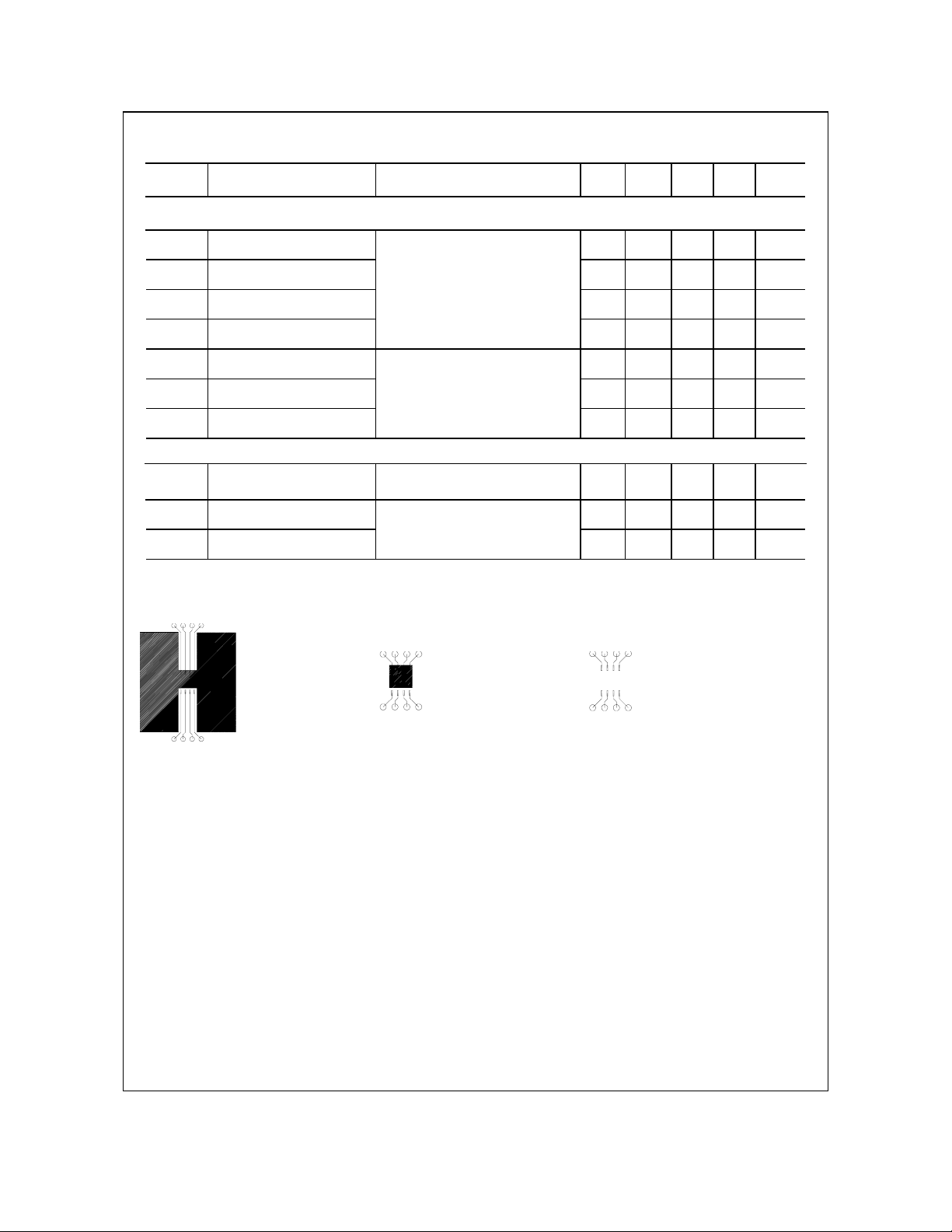
Electrical Characteristics T
= 25°C unless otherwise noted
A
Symbol Parameter Test Conditions Type Min Typ Max Units
Drain-Source Avalanche Ratings (Note 3)
E
Drain-Source Avalanche
AS
I
Drain-Source Avalanche
AS
Energy (Single Pulse)
Current
VDD = 40 V, ID = 7.3 A, L = 1 mH Q1 27 mJ
= –40 V, ID =–8.7 A, L = 1 mH Q2 38 mJ
V
DD
Q1
Q2
7.3
–8.7
A
Off Characteristics
Q1
40
BV
Drain-Source Breakdown
DSS
ΔBVDSS
ΔT
I
Zero Gate Voltage Drain
DSS
I
Gate-Body Leakage
GSS
Voltage
Breakdown Voltage
Temperature Coefficient
J
Current
= 0 V, ID = 250 μA
V
GS
= 0 V, ID = –250 μA
V
GS
= 250 μA, Referenced to 25°C
I
D
= –250 µA, Referenced to 25°C
I
D
VDS = 32 V, VGS = 0 V
= –32 V, VGS = 0 V
V
DS
= ±20 V, VDS = 0 V
V
GS
Q2
–40
Q1
Q2
Q1
Q2
All
V
34
–40
1
–1
±100
mV/°C
μA
nA
On Characteristics (Note 2)
V
Gate Threshold Voltage
GS(th)
ΔVGS(th)
ΔTJ
R
DS(on)
gFS Forward Transconductance VDS = 10 V, ID = 6.2 A
Gate Threshold Voltage
Temperature Coefficient
Static Drain-Source
On-Resistance
= VGS, ID = 250 μA
V
DS
= VGS, ID = –250 µA
V
DS
= 250 μA, Referenced to 25°C
I
D
I
= –250 µA, Referenced to 25°C
D
VGS = 10 V, ID = 6.2 A
= 4.5 V, ID = 4.8 A
V
GS
= 10 V, ID = 6.2 A, TJ = 125°C
V
GS
= –10 V, ID = –4.4 A
V
GS
= –4.5 V, ID = –3.8 A
V
GS
= –10 V, ID = –4.4 A, TJ = 125°C
V
GS
= –10 V, ID =–4.4 A
V
DS
Q1
Q2 1 –1
Q1
Q2
Q1 21
Q2 37
Q1
Q2
1.9
–1.7 3 –3
–5 4
26
29
50
55
21
12
V
mV/°C
29
mΩ
36
43
46
63
73
S
Dynamic Characteristics
C
Input Capacitance Q1
iss
C
Output Capacitance Q1
oss
C
Reverse Transfer
rss
RG Gate Resistance f = 1.0 MHz
Capacitance
Q1
= 20 V, VGS = 0 V, f = 1.0 MHz
V
DS
Q2
= –20 V, VGS = 0 V, f = 1.0 MHz
V
DS
Q2
Q2
Q1
Q2
Q1
Q2
760
1050
100
140
60
70
1.2 9
pF
pF
pF
Ω
4
7
D
l N
Ph
nn
l P
w
rTr
n
h
®
M
FET
FDS4897C Rev C(W) www.fairchildsemi.com
Page 3
S
89
C
ua
&
C
a
e
o
e
e
c
OS
FD
Electrical Characteristics (continued) T
Symbol
Parameter
Test Conditions
= 25°C unless otherwise noted
A
Type Min Typ Max Units
Switching Characteristics (Note 2)
t
Turn-On Delay Time
d(on)
tr Turn-On Rise Time
t
d(off)
tf Turn-Off Fall Time
Qg Total Gate Charge
Qgs Gate-Source Charge
Qgd Gate-Drain Charge
Turn -Off Del a y Time
Q1
= 20 V, ID = 1 A,
V
DD
= 10V, R
V
GS
Q2
= –20 V, ID = –1 A,
V
DD
= –10V, R
V
GS
Q1
= 20 V, ID = 6.2 A, VGS = 10 V
V
DS
Q2
= –20 V, ID = –4.4 A,VGS =–10 V
V
DS
GEN
GEN
= 6 Ω
= 6 Ω
Q1
Q2
Q1
Q2
Q1
Q2
Q1
Q2
Q1
Q2
Q1
Q2
Q1
Q2
9
12
5
15
23
45
3
18 6 32
14
20
2.4 3 nC
2.8 4 nC
Drain–Source Diode Characteristics
VSD Drain-Source Diode Forward
trr Diode Reverse Recovery
Qrr Diode Reverse Recovery
Notes:
1. R
θJA
the drain pins. R
Voltage
Time
Charge
is the sum of the junction-to-case and case-to-ambient thermal resistance where the case thermal reference is defined as the solder mounting surface of
is guaranteed by design while R
θJC
VGS = 0 V, IS = 1.3 A (Note 2)
VGS = 0 V, IS = –1.3 A (Note 2)
Q1
= 6.2 A, diF/dt = 100 A/µs
I
F
Q2
= –4.4 A, diF/dt = 100 A/µs
I
F
is determined by the user's board design.
θCA
Q1
Q2
Q1
Q2
Q1
Q2
0.7
–0.7
–1.2
17
24
7
12
1.2
18
22
10
27
37
72
20
28
ns
ns
ns
ns
nC
V
ns
nC
4
7
D
l N
Ph
nn
l P
w
rTr
n
h
®
M
a) 78°C/W when
mounted on a
0.5 in2 pad of 2 oz
copper
Scale 1 : 1 on letter size paper
2. Pulse Test: Pulse Width < 300μs, Duty Cycle < 2.0%
3. BV(avalanche) Single-Pulse rating is guaranteed by design if device is operated within the UIS SOA boundary of the device.
b) 125°C/W when
mounted on a .02 in2
pad of 2 oz copper
c) 135°C/W when mounted on a
minimum pad.
FET
FDS4897C Rev C(W) www.fairchildsemi.com
Page 4

S
89
C
ua
&
C
a
e
o
e
e
c
OS
FD
Typical Characteristics: Q1 (N-Channel)
20
VGS = 10V
16
12
8
, DRAIN CURRENT (A)
D
I
4
0
0 0.5 1 1.5 2 2.5
4.0V
3.5V
4.5V6.0V
V
, DRAIN TO SOURCE VOLTAGE (V)
DS
3.0V
Figure 1. On-Region Characteristics. Figure 2. On-Resistance Variation with
1.6
ID = 7.0A
V
= 10V
GS
1.4
1.2
, NORMALIZED
1
DS(ON)
R
0.8
DRAIN-SOURCE ON-RESISTANCE
0.6
-50 -25 0 25 50 75 100 125 150
T
, JUNCTION TEMPERATURE (oC)
J
Figure 3. On-Resistance Variation with
Temperature.
3
2.6
2.2
1.8
, NORMALIZED
1.4
DS(ON)
R
1
DRAIN-SOURCE ON-RESISTANCE
0.6
0 4 8 12 16 20
3.5V
VGS = 3.0V
4.0V
, DRAIN CURRENT (A)
I
D
4.5V
Drain Current and Gate Voltage.
0.07
0.06
0.05
0.04
0.03
, ON-RESISTANCE (OHM)
TA = 25oC
DS(ON)
0.02
R
0.01
246810
TA = 125oC
, GATE TO SOURCE VOLTAGE (V)
V
GS
Figure 4. On-Resistance Variation with
Gate-to-Source Voltage.
6.0V
10V
ID = 3.5A
4
7
D
l N
Ph
nn
l P
w
rTr
n
h
®
M
FET
20
VDS = 10V
15
10
TA = 125oC
, DRAIN CURRENT (A)
D
I
5
0
11.522.533.5
V
, GATE TO SOURCE VOLTAGE (V)
GS
-55oC
25oC
100
VGS = 0V
10
1
0.1
0.01
0.001
, REVERSE DRAIN CURRENT (A)
S
I
0.0001
0 0.2 0.4 0.6 0.8 1 1.2
V
TA = 125oC
25oC
BODY DIODE FORWARD VOLTAGE (V)
SD,
-55oC
Figure 5. Transfer Characteristics. Figure 6. Body Diode Forward Voltage Variation
with Source Current and Temperature.
FDS4897C Rev C(W) www.fairchildsemi.com
Page 5

S
89
C
ua
&
C
a
e
o
e
e
c
OS
FD
Typical Characteristics: Q1 (N-Channel)
10
ID = 7A
8
6
4
2
, GATE-SOURCE VOLTAGE (V)
GS
V
0
0481216
Q
g
VDS = 10V
30V
20V
, GATE CHARGE (nC)
Figure 7. Gate Charge Characteristics. Figure 8. Capacitance Characteristics.
100
R
LIMIT
DS(ON)
10
10ms
DC
10s
1s
100ms
1
, DRAIN CURRENT (A)
VGS = 10.0V
D
0.1
I
SINGLE PULSE
= 135oC/W
R
JA
θ
= 25oC
T
0.01
A
0.1 1 10 100
, DRAIN-SOURCE VOLTAGE (V)
V
DS
100μs
1ms
Figure 9. Maximum Safe Operating Area. Figure 10. Single Pulse Maximum
1000
800
600
400
CAPACITANCE (pF)
200
C
rss
0
0 5 10 15 20 25 30 35 40
50
40
30
20
10
P(pk), PEAK TRANSIENT POWER (W)
0
0.001 0.01 0.1 1 10 100 1000
C
oss
, DRAIN TO SOURCE VOLTAGE (V)
V
DS
, TIME (sec)
t
1
Power Dissipation.
C
iss
SINGLE PULSE
R
JA
θ
T
f = 1 MHz
V
= 0 V
GS
= 135°C/W
= 25°C
A
4
7
D
l N
Ph
nn
l P
w
rTr
n
h
®
M
FET
50
SINGLE PULSE
R
= 135°C/W
θ
40
30
20
10
I(pk), PEAK TRANSIENT CURRENT (A)
0
0.001 0.01 0.1 1 10 100 1000
, TIME (sec)
t
1
JA
T
= 25°C
A
Figure 11. Single Pulse Maximum Peak
Current.
FDS4897C Rev C(W) www.fairchildsemi.com
100
TJ = 25oC
10
, AVALANCHE CURRENT (A)
(AS)
I
1
0.01 0.1 1 10
, TIME IN AVANCHE(ms)
t
AV
Figure 12. Unclamped Inductive Switching
Capability.
Page 6

S
89
C
ua
&
C
a
e
o
e
e
c
OS
FD
Typical Characteristics: Q2 (P-Channel)
30
VGS = -10V -6.0V
25
20
15
10
, DRAIN CURRENT (A)
D
-I
5
0
00.511.522.533.544.5
, DRAIN TO SOURCE VOLTAGE (V)
-V
DS
-4.5V
-4.0V
-3.5V
-3.0V
Figure 13. On-Region Characteristics. Figure 14. On-Resistance Variation with
1.6
ID = -4.4A
1.5
= - 10V
V
GS
1.4
1.3
1.2
1.1
, NORMALIZED
1
0.9
DS(ON)
R
0.8
0.7
DRAIN-SOURCE ON-RESISTANCE
0.6
-50-250 255075100125150
, JUNCTION TEMPERATURE (oC)
T
J
Figure 15. On-Resistance Variation with
Temperature.
2.6
2.4
2.2
VGS = - 3.5V
2
1.8
1.6
, NORMALIZED
1.4
DS(ON)
R
1.2
1
DRAIN-SOURCE ON-RESISTANCE
0.8
0 5 10 15 20 25 30
-4.0V
-4.5V
-I
, DRAIN CURRENT (A)
D
-6.0V
Drain Current and Gate Voltage.
0.14
0.12
0.1
0.08
0.06
, ON-RESISTANCE (OHM)
TA = 25oC
DS(ON)
0.04
R
0.02
246810
TA = 125oC
-V
, GATE TO SOURCE VOLTAGE (V)
GS
Figure 16. On-Resistance Variation with
Gate-to-Source Voltage.
-10V
ID = -2.2A
4
7
D
l N
Ph
nn
l P
w
rTr
n
h
®
M
FET
25
VDS = -10V
20
15
10
, DRAIN CURRENT (A)
D
-I
5
0
1.522.533.544.5
-V
, GATE TO SOURCE VOLTAGE (V)
GS
TA = -55oC
25oC
125oC
100
VGS = 0V
10
1
0.1
0.01
0.001
, REVERSE DRAIN CURRENT (A)
S
-I
0.0001
0 0.2 0.4 0.6 0.8 1 1.2
TA = 125oC
25oC
-V
BODY DIODE FORWARD VOLTAGE (V)
SD,
-55oC
Figure 17. Transfer Characteristics. Figure 18. Body Diode Forward Voltage Variation
with Source Current and Temperature.
FDS4897C Rev C(W) www.fairchildsemi.com
Page 7

μ
S
89
C
ua
&
C
a
e
o
e
e
c
OS
FD
Typical Characteristics: Q2 (P-Channel)
10
ID = -4.4A
8
6
4
2
, GATE-SOURCE VOLTAGE (V)
GS
-V
0
0 5 10 15 20 25
VDS = -10V
, GATE CHARGE (nC)
Q
g
-20V
-30V
Figure 19. Gate Charge Characteristics. Figure 20. Capacitance Characteristics.
100
R
LIMIT
DS(ON)
10
10ms
100ms
1
, DRAIN CURRENT (A)
D
-I
0.01
VGS = -10V
SINGLE PULSE
0.1
R
= 135oC/W
JA
θ
= 25oC
T
A
0.1 1 10 100
-V
, DRAIN-SOURCE VOLTAGE (V)
DS
1s
10s
DC
100
1ms
Figure 21. Maximum Safe Operating Area. Figure 22. Single Pulse Maximum
1400
1200
1000
800
600
400
CAPACITANCE (pF)
200
0
50
40
30
20
10
P(pk), PEAK TRANSIENT POWER (W)
0
0.001 0.01 0.1 1 10 100 1000
C
OSS
C
RSS
0 5 10 15 20 25 30 35 40
-V
DS
C
ISS
, DRAIN TO SOURCE VOLTAGE (V)
, TIME (sec)
t
1
Power Dissipation.
f = 1 MHz
= 0 V
V
GS
SINGLE PULSE
= 135°C/W
R
JA
θ
= 25°C
T
A
4
7
D
l N
Ph
nn
l P
w
rTr
n
h
®
M
FET
40
30
20
10
P(pk), PEAK TRANSIENT CURRENT (A)
0
0.001 0.01 0.1 1 10 100 1000
t
, TIME (sec)
1
SINGLE PULSE
R
= 135°C/W
θ
JA
T
= 25°C
A
Figure 23. Single Pulse Maximum Peak
Current
100
TJ = 25oC
10
, AVALANCHE CURRENT (A)
(AS)
I
1
0.01 0.1 1 10
t
, TIME IN AVANCHE(ms)
AV
Figure 24. Unclamped Inductive Switching
Capability
FDS4897C Rev C(W) www.fairchildsemi.com
Page 8

)
S
89
C
ua
&
C
a
e
o
e
e
c
OS
Typical Characteristics : N and P-Channel
1
D = 0.5
0.2
0.1
0.1
0.01
r(t), NORMALIZED EFFECTIVE
0.001
TRANSIENT THERMAL RESISTANCE
0.05
0.02
0.01
SINGLE PULSE
0.0001 0.001 0.01 0.1 1 10 100 1000
, TIME (sec)
t
1
Figure 25. Transient Thermal Response Curve.
Thermal characterization performed using the conditions described in Note 1c.
Transient thermal response will change depending on the circuit board design.
R
(t) = r(t) * R
JA
θ
R
= 135oC/W
JA
θ
P(pk
t
1
t
2
T
- TA = P * R
J
Duty Cycle, D = t
FD
4
7
D
l N
JA
θ
Ph
(t)
JA
θ
/ t
1
2
nn
l P
w
rTr
n
h
®
M
FET
FDS4897C Rev C(W) www.fairchildsemi.com
Page 9

TRADEMARKS
The following are registered and unregistered trademarks Fairchild Semiconductor owns or is authorized to use and is
not intended to be an exhaustive list of all such trademarks.
ACEx™
ActiveArray™
Bottomless™
FPS™
Build it Now™
CoolFET™
CROSSVOLT™
DOME™
EcoSPARK™
2
E
CMOS™
EnSigna™
FACT™
FACT Quiet Series™
Across the board. Around the world.™
The Power Franchise
Programmable Active Droop™
DISCLAIMER
FAIRCHILD SEMICONDUCTOR RESERVES THE RIGHT TO MAKE CHANGES WITHOUT FURTHER NOTICE T O ANY
PRODUCTS HEREIN TO IMPROVE RELIABILITY , FUNCTION OR DESIGN. FAIRCHILD DOES NOT ASSUME ANY LIABILITY
ARISING OUT OF THE APPLICATION OR USE OF ANY PRODUCT OR CIRCUIT DESCRIBED HEREIN; NEITHER DOES IT
CONVEY ANY LICENSE UNDER ITS PA TENT RIGHTS, NOR THE RIGHTS OF OTHERS.
LIFE SUPPORT POLICY
®
FAST
FAST r™
LittleFET™
FRFET™
GlobalOptoisolator™
GTO™
HiSeC™
2
I
C™
i-Lo™
ImpliedDisconnect™
IntelliMAX™
®
ISOPLANAR™
MICROCOUPLER™
MicroFET™
MicroPak™
MICROWIRE™
MSX™
MSXPro™
OCX™
OCXPro™
OPTOLOGIC
®
OPTOPLANAR™
PACMAN™
POP™
Power247™
PowerEdge™
PowerSaver™
PowerTrench
®
QFET
®
QS™
QT Optoelectronics™
Quiet Series™
RapidConfigure™
RapidConnect™
μSerDes™
ScalarPump™
SILENT SWITCHER
SMART ST ART™
SPM™
Stealth™
SuperFET™
SuperSOT™-3
SuperSOT™-6
SuperSOT™-8
SyncFET™
TinyLogic
TINYOPTO™
TruTranslation™
UHC™
UltraFET
UniFET™
VCX™
®
Wire™
®
®
FAIRCHILD’S PRODUCTS ARE NOT AUTHORIZED FOR USE AS CRITICAL COMPONENTS IN LIFE SUPPORT
DEVICES OR SYSTEMS WITHOUT THE EXPRESS WRITTEN APPROVAL OF FAIRCHILD SEMICONDUCTOR CORPORA TION.
As used herein:
1. Life support devices or systems are devices or
systems which, (a) are intended for surgical implant into
the body, or (b) support or sustain life, or (c) whose
failure to perform when properly used in accordance
with instructions for use provided in the labeling, can be
reasonably expected to result in significant injury to the
user.
PRODUCT STA TUS DEFINITIONS
Definition of Terms
Datasheet Identification Product Status Definition
Advance Information
Preliminary
No Identification Needed
Formative or
In Design
First Production
Full Production
2. A critical component is any component of a life
support device or system whose failure to perform can
be reasonably expected to cause the failure of the life
support device or system, or to affect its safety or
effectiveness.
This datasheet contains the design specifications for
product development. Specifications may change in
any manner without notice.
This datasheet contains preliminary data, and
supplementary data will be published at a later date.
Fairchild Semiconductor reserves the right to make
changes at any time without notice in order to improve
design.
This datasheet contains final specifications. Fairchild
Semiconductor reserves the right to make changes at
any time without notice in order to improve design.
Obsolete
Not In Production
This datasheet contains specifications on a product
that has been discontinued by Fairchild semiconductor.
The datasheet is printed for reference information only.
Rev. I17
 Loading...