

Page 1
查询FDB6670AS供应商查询FDB6670AS供应商
January 2005
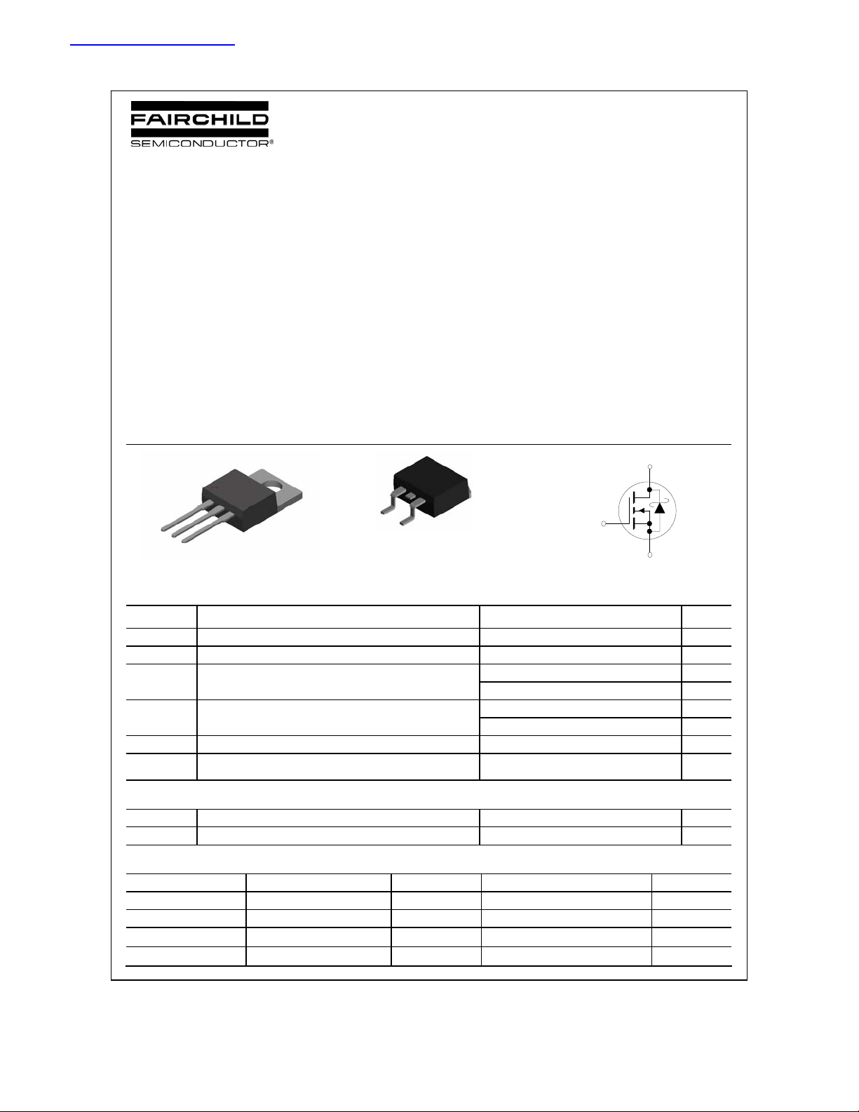
FDP6670AS/FDB6670AS
30V N-Channel PowerTrench® SyncFET™
FDP6670AS/FDB6670AS
General Description
This MOSFET is designed to replace a single MOSFET
and parallel Schottky diode in synchronous DC:DC
power supplies. This 30V MOSFET is designed to
maximize power conversion efficiency, providing a low
and low gate charge. The FDP6670AS
R
DS(ON)
Features
• 31 A, 30 V. R
R
• Includes SyncFET Schottky body diode
= 8.5 mΩ @ VGS = 10 V
DS(ON)
= 10.5 mΩ @ VGS = 4.5 V
DS(ON)
includes an integrated Schottky diode using Fairchild’s
monolithic SyncFET technology. The performance of
• Low gate charge (28nC typical)
the FDP6670AS/FDB6670AS as the low-side switch in
a synchronous rectifier is indistinguishable from the
performance of the FDP6670A/FDB6670A in parallel
with a Schottky diode.
G
G
D
S
TO-220
FDP Series
Absolute Maximum Ratings T
S
o
=25
C unless otherwise noted
A
• High performance trench technology for extremely
low R
and fast switching
DS(ON)
• High power and current handling capability
D
G
D
TO-263AB
FDB Series
S
Symbol Parameter Ratings Units
V
Drain-Source Voltage 30 V
DSS
V
Gate-Source Voltage
GSS
ID Drain Current – Continuous
– Pulsed (Note 1)
PD
TJ, T
STG
Total Power Dissipation @ T
Derate above 25°C
Operating and Storage Junction Temperature Range –55 to +150
= 25°C
C
TL Maximum lead temperature for soldering purposes,
1/8” from case for 5 seconds
±20
62
150
62.5
0.5
275
W/°C
V
A
W
°C
°C
Thermal Characteristics
R
θJC
R
θJA
Thermal Resistance, Junction-to-Case
Thermal Resistance, Junction-to-Ambient
2.1
62.5
°C/W
°C/W
Package Marking and Ordering Information
Device Marking Device Reel Size Tape width Quantity
FDB6670AS FDB6670AS 13’’ 24mm 800 units
FDB6670AS FDB6670AS_NL (Note 3) 13’’ 24mm 800 units
FDP6670AS FDP6670AS Tube n/a 45
FDP6670AS FDP6670AS_NL (Note 4) Tube n/a 45
©2005 Fairchild Semiconductor Corporation
FDP6670AS/FDB6670AS Rev A(X)
Page 2
A
FDP6670
Electrical Characteristics T
= 25°C unless otherwise noted
A
Symbol Parameter Test Conditions Min Typ Max Units
Off Characteristics
BV
Drain–Source Breakdown Voltage VGS = 0 V, ID = 1mA 30 V
DSS
∆BVDSS
∆T
I
Zero Gate Voltage Drain Current VDS = 24 V, VGS = 0 V 500 µA
DSS
I
Gate–Body Leakage
GSS
Breakdown Voltage Temperature
Coefficient
J
= 26mA, Referenced to 25°C
I
D
= ±20 V, VDS = 0 V
V
GS
30
±100
mV/°C
nA
On Characteristics (Note 2)
V
Gate Threshold Voltage VDS = VGS, ID = 1mA 1 1.7 3 V
GS(th)
∆VGS(th)
∆TJ
R
DS(on)
I
D(on)
Gate Threshold Voltage
Temperature Coefficient
Static Drain–Source
On–Resistance
I
= 26mA, Referenced to 25°C
D
VGS = 10 V, ID = 31 A
= 4.5 V, ID = 26.5 A
V
GS
V
=10 V, ID =31 A, TJ=125°C
GS
On–State Drain Current VGS = 10 V, VDS = 10 V 60 A
–3.4
6.8
8.4
9
8.5
10.5
mV/°C
mΩ
12.5
gFS Forward Transconductance VDS = 10 V, ID = 31 A 84 S
Dynamic Characteristics
C
Input Capacitance 1570 pF
iss
C
Output Capacitance 440 pF
oss
C
Reverse Transfer Capacitance
rss
RG Gate Resistance VGS = 15 mV, f = 1.0 MHz 1.9
V
= 15 V, V
DS
f = 1.0 MHz
= 0 V,
GS
160 pF
Ω
Switching Characteristics (Note 2)
t
Turn–On Delay Time 9 18 ns
d(on)
tr Turn–On Rise Time 12 22 ns
t
Turn–Off Dela y Time 27 43 ns
d(off)
tf Turn–Off Fall Time
t
Turn–On Delay Time 16 29 ns
d(on)
tr Turn–On Rise Time 16 29 ns
t
Turn–Off Dela y Time 25 40 ns
d(off)
tf Turn–Off Fall Time
Qg Total Gate Charge, Vgs=10V 28 39 nC
Qgs Gate–Source Charge, Vgs=5V 15 21 nC
Qgd Gate–Drain Charge 5 nC
Qgd Gate–Drain Charge
V
= 15 V, ID = 1 A,
DS
= 10 V, R
V
GS
V
= 15 V, ID = 1 A,
DS
= 4.5 V, R
V
GS
V
= 15 V, ID = 31 A,
DS
GEN
GEN
= 6 Ω
19 34 ns
= 6 Ω
13 23 ns
5 nC
S/FDB6670AS
Drain–Source Diode Characteristics
VSD Drain–Source Diode Forward
Voltage
trr Diode Reverse Recovery Time 20 nS
Qrr Diode Reverse Recovery Charge
Notes:
1. Pulse Test: Pulse Width < 300µs, Duty Cycle < 2.0%
2. See “SyncFET Schottky body diode characteristics” below.
3. FDB6670AS_NL is a lead free product. The FDB6670AS_NL marking will appear on the reel label.
4. FDP6670AS_NL is a lead free product. The FDP6670AS_NL marking will appear on the reel label.
VGS = 0 V, IS = 3.5 A (Note 1)
VGS = 0 V, IS = 7 A (Note 1)
= 3.5 A,
I
F
= 300 A/µs (Note 2)
d
iF/dt
0.5
14 nC
0.7
0.6
0.9
FDP6670AS/FDB6670AS Rev A (X)
V
Page 3

A
Typical Characteristics
150
VGS = 10V
120
, DRAIN CURRENT (A)
D
I
6.0V
90
60
30
0
01234
V
, DRAIN-SOURCE VOLTAGE (V)
DS
4.5V
5.0V
4.0V
3.5V
3.0V
Figure 1. On-Region Characteristics. Figure 2. On-Resistance Variation with
1.8
VGS = 3.5V
1.6
1.4
4.0V
, NORMALIZED
1.2
DS(ON)
R
1
DRAIN-SOURCE ON-RESISTA NCE
0.8
0 30 60 90 120 150
4.5V
5.0V
I
, DRAIN CURRENT (A)
D
Drain Current and Gate Voltage.
FDP6670
S/FDB6670AS
6.0V
10V
1.6
ID = 31A
V
= 10V
GS
1.4
1.2
, NORMALIZED
1
DS(ON)
R
0.8
DRAIN-SOURCE ON-RESISTANCE
0.6
-50-250 255075100125150
T
, JUNCTION TEMPERATURE (oC)
J
Figure 3. On-Resistance Variation with
Temperature.
80
VDS = 5V
60
40
, DRAIN CURRENT (A)
D
20
I
0
1.522.533.54
TA = 125oC
-55oC
25oC
V
, GATE TO SOURCE VOLTAGE (V)
GS
0.022
0.017
0.012
, ON-RESISTANCE (OHM)
0.007
DS(ON)
R
0.002
TA = 25oC
246810
V
GS
TA = 125oC
, GATE TO SOURCE VOLTAGE (V)
Figure 4. On-Resistance Variation with
Gate-to-Source Voltage.
10
VGS = 0V
1
TA = 125oC
0.1
, REVERSE DRAIN CURRENT (A)
S
I
0.01
0 0.1 0.2 0.3 0.4 0.5 0.6
, BODY DIODE FORWARD VOLTAGE (V)
V
SD
25oC
-55oC
Figure 5. Transfer Characteristics. Figure 6. Body Diode Forward Voltage Variation
with Source Current and Temperature.
ID = 15.5A
FDP6670AS/FDB6670AS Rev A (X)
Page 4

A
Typical Characteristics (continued)
10
ID = 31A
8
6
4
2
, GATE-SOURCE VOLTAGE (V)
GS
V
0
0 6 12 18 24 30
VDS = 10V
Q
, GATE CHARGE (nC)
g
20V
15V
Figure 7. Gate Charge Characteristics. Figure 8. Capacitance Characteristics.
2400
1800
C
iss
1200
C
CAPACITANCE (pF)
600
C
rss
0
0 5 10 15 20 25 30
oss
V
, DRAIN TO SOURCE VOLTAGE (V)
DS
f = 1MHz
= 0 V
V
GS
FDP6670
S/FDB6670AS
1000
100µs
10ms
100m
1s
, DRAIN CURRENT (A)
I
100
10
D
R
LIMIT
DS(ON)
VGS = 10V
SINGLE PULSE
= 2.1oC/W
R
θ
JC
= 25oC
T
A
10s
DC
1
0.1 1 10 100
, DRAIN-SOURCE VOLTAGE (V)
V
DS
1000
800
600
400
200
P(pk), PEAK TRANSIENT POWER (W)
0
0.1 1 10 100 1000
, TIME (sec)
t
1
Figure 9. Maximum Safe Operating Area. Figure 10. Single Pulse Maximum
Power Dissipation.
1
D = 0.5
0.2
0.1
0.01
r(t), NORMALIZED EFFECTIVE
TRANSIENT THERMAL RESISTANCE
0.001
0.1
0.05
0.02
0.01
SINGLE PULSE
0.0001 0.001 0.01 0.1 1 10 100 1000
, TIME (sec)
t
1
R
(t) = r(t) * R
JC
θ
R
= 2.1 °C/W
JC
θ
P(pk
t
1
t
2
- Tc = P * R
T
J
Duty Cycle, D = t
Figure 11. Transient Thermal Response Curve.
Thermal characterization performed using the conditions described in Note 1c.
Transient thermal response will change depending on the circuit board design.
JC
θ
(t)
JC
θ
/ t
1
2
SINGLE PULSE
= 2.1°C/W
R
θ
JC
T
= 25°C
A
FDP6670AS/FDB6670AS Rev A (X)
Page 5

A
Typical Characteristics (continued)
FDP6670
SyncFET Schottky Body Diode
Characteristics
Fairchild’s SyncFET process embeds a Schottky diode
in parallel with PowerTrench MOSFET. This diode
exhibits similar characteristics to a discrete external
Schottky diode in parallel with a MOSFET. Figure 12
FDP6670AS.
CURRENT: 0.8A/div
Figure 12. FDP6670AS SyncFET body
diode reverse recovery characteristic.
For comparison purposes, Figure 13 shows the reverse
recovery characteristics of the body diode of an
equivalent size MOSFET produced without SyncFET
(FDP6670A).
TIME: 12.5ns/div
Schottky barrier diodes exhibit significant leakage at
high temperature and high reverse voltage. This will
increase the power in the device.
0.1
0.01
0.001
0.0001
, REVERSE LEAKAGE CURRENT (A)
DSS
I
0.00001
0 102030
TA = 125oC
TA = 100oC
TA = 25oC
V
, REVERSE VOLTAGE (V)
DS
Figure 14. SyncFET diode reverse leakage
versus drain-source voltage and
temperature.
S/FDB6670AS
CURRENT: 0.8A/div
TIME: 12.5ns/div
Figure 13. Non-SyncFET (FDP6670A) body
diode reverse recovery characteristic.
FDP6670AS/FDB6670AS Rev A (X)
Page 6

TRADEMARKS
The following are registered and unregistered trademarks Fairchild Semiconductor owns or is authorized to use and is
not intended to be an exhaustive list of all such trademarks.
ACEx™
ActiveArray™
Bottomless™
FPS™
CoolFET™
CROSSVOL T™
DOME™
EcoSPARK™
E2CMOS™
EnSigna™
FACT™
FACT Quiet Series™
Across the board. Around the world.™
The Power Franchise
Programmable Active Droop™
DISCLAIMER
FAIRCHILD SEMICONDUCTOR RESERVES THE RIGHT TO MAKE CHANGES WITHOUT FURTHER NOTICE T O ANY
PRODUCTS HEREIN TO IMPROVE RELIABILITY , FUNCTION OR DESIGN. FAIRCHILD DOES NOT ASSUME ANY LIABILITY
ARISING OUT OF THE APPLICATION OR USE OF ANY PRODUCT OR CIRCUIT DESCRIBED HEREIN; NEITHER DOES IT
CONVEY ANY LICENSE UNDER ITS PA TENT RIGHTS, NOR THE RIGHTS OF OTHERS.
LIFE SUPPORT POLICY
FAST
FASTr™
LittleFET™
FRFET™
GlobalOptoisolator™
GTO™
HiSeC™
I2C™
i-Lo™
ImpliedDisconnect™
IntelliMAX™
ISOPLANAR™
MICROCOUPLER™
MicroFET™
MicroPak™
MICROWIRE™
MSX™
MSXPro™
OCX™
OCXPro™
OPTOLOGIC
OPTOPLANAR™
P ACMAN™
POP™
Power247™
PowerEdge™
PowerSaver™
PowerTrench
QFET
QS™
QT Optoelectronics™
Quiet Series™
RapidConfigure™
RapidConnect™
µSerDes™
SILENT SWITCHER
SMART ST ART™
SPM™
Stealth™
SuperFET™
SuperSOT™-3
SuperSOT™-6
SuperSOT™-8
SyncFET™
TinyLogic
TINYOPTO™
TruTranslation™
UHC™
UltraFET
UniFET™
VCX™
FAIRCHILD’S PRODUCTS ARE NOT AUTHORIZED FOR USE AS CRITICAL COMPONENTS IN LIFE SUPPORT
DEVICES OR SYSTEMS WITHOUT THE EXPRESS WRITTEN APPROVAL OF FAIRCHILD SEMICONDUCTOR CORPORA TION.
As used herein:
1. Life support devices or systems are devices or
systems which, (a) are intended for surgical implant into
the body, or (b) support or sustain life, or (c) whose
failure to perform when properly used in accordance
with instructions for use provided in the labeling, can be
reasonably expected to result in significant injury to the
user.
PRODUCT STA TUS DEFINITIONS
Definition of Terms
Datasheet Identification Product Status Definition
Advance Information
Preliminary
No Identification Needed
Formative or
In Design
First Production
Full Production
2. A critical component is any component of a life
support device or system whose failure to perform can
be reasonably expected to cause the failure of the life
support device or system, or to affect its safety or
effectiveness.
This datasheet contains the design specifications for
product development. Specifications may change in
any manner without notice.
This datasheet contains preliminary data, and
supplementary data will be published at a later date.
Fairchild Semiconductor reserves the right to make
changes at any time without notice in order to improve
design.
This datasheet contains final specifications. Fairchild
Semiconductor reserves the right to make changes at
any time without notice in order to improve design.
Obsolete
Not In Production
This datasheet contains specifications on a product
that has been discontinued by Fairchild semiconductor.
The datasheet is printed for reference information only.
Rev. I15
 Loading...