

Page 1
FAN8408D
2 Phase Half Wave BLDC Motor Driver
www.fairchildsemi.com
Features
• A wide range of operation voltage: 4V to 15V
• Built-in motor lock detector.
• Automatic restart function
• Hall output for a motor speed detection
• Built-in thermal shut down circuits
• Built-in reverse current protection diode
• Compact package: 8-SOP-225
Description
The FAN8408D is a monolithic integrated circuit, and
suitable for DC cooling fan motors.
8-SOP-225
1
Typical Applications
• DC cooling fan motor
©2002 Fairchild Semiconductor Corporation
Ordering Information
Device Package Operating Temp.
FAN8408D 8-SOP-225 −25°C ~ 85°C
FAN8408DTF 8-SOP-225 −25°C ~ 85°C
Rev.1.0.4
Page 2
FAN8408D
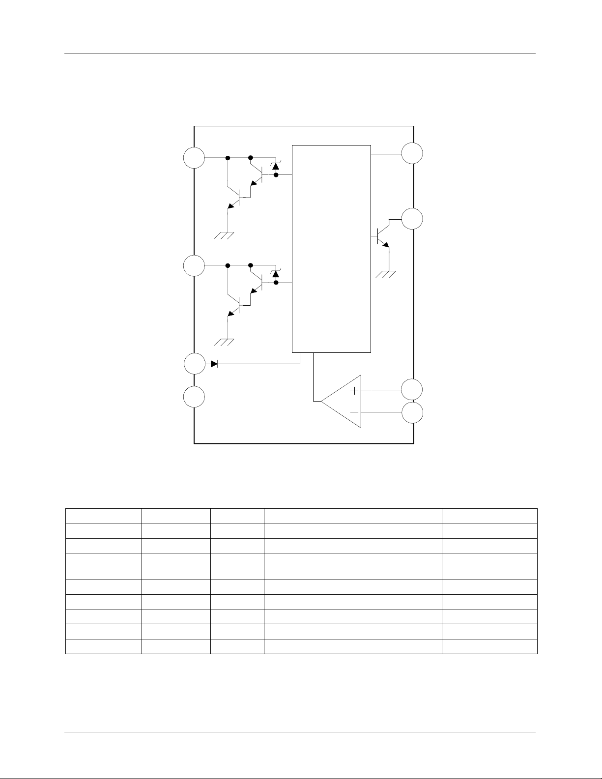
Block Diagram
OUT
OUT
LD
1
B
3
HO
2
Commutation &
Control
7
A
& TSD
V
GND
CC
4
IN+
8
5
IN-
6
Pin Definitions
Pin Number Pin Name I/O Pin Function Description Remark
1OUT
B
2 HO O Hall output Open Collector
3LD4V
CC
5IN+ I Hall input + -
6IN− I Hall input − -
7OUT
A
8 GND - Ground -
O Motor output B -
Triangle pulse generator for lock detector
and automatic restart
- Supply voltage -
O Motor output A -
-
2
Page 3
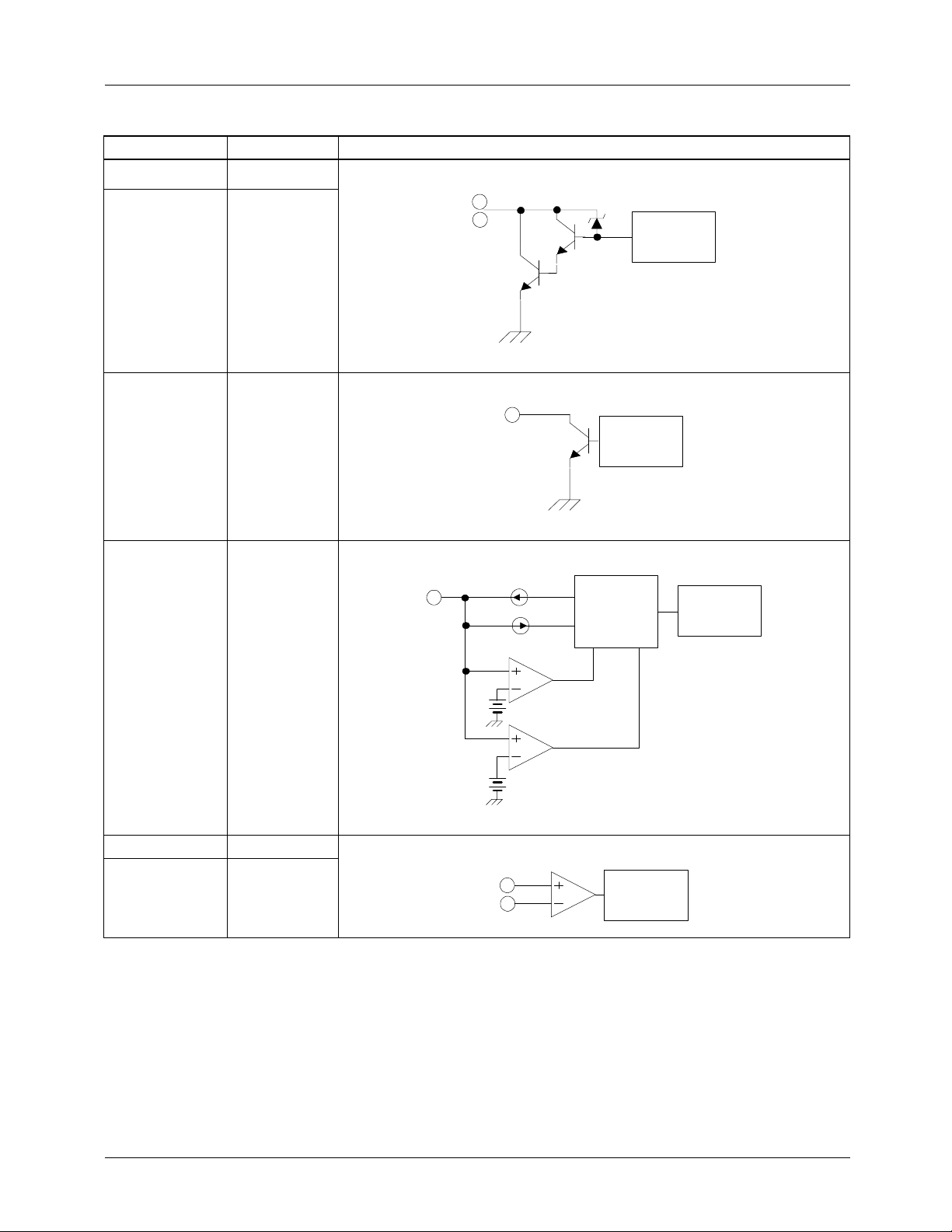
Equivalent Circuits
Description Pin No. Internal Circuit
OUT
B
1
FAN8408D
OUT
A
HO
LD 3
7
1
7
Commutation
2
2
Commutation
3
Lock detector
& Automatic
restart
Commutation
IN+ 5
IN- 6
V
LDCP
V
LDCL
5
6
Commutation
3
Page 4
FAN8408D
Absolute Maximum Ratings (Ta = 25°C)
Parameter Symbol Value Unit
Maximum power supply voltage V
Maximum power dissipation
Thermal resistance
note1
note1
Maximum output voltage V
Maximum output current I
Hall output current I
Hall output withstanding voltage V
Maximum hall input ac level V
Operating temperature T
Storage temperature T
Note1:
PCB Condition: Thickness(1.6mm), Dimension(76.2mm * 114.3mm)
Refer: EIA/J SED 51-3 & EIA/J SED 51-7
Note2: Air condition (0m/s)
Note3: Air condition (3m/s)
Note4: Should not exceed P
or ASO value
D
CCMAX
P
DMAX
Θ
JA
OMAX
OMAX
HO
HO
HACMAX
OPR
STG
18 V
note2
429
620
291.61
201.52
note3
note2
note3
mW
°C/W
30 V
note4
1.2
A
10 mA
36 V
6V
−25 ~ 85 °C
−55 ~ 150 °C
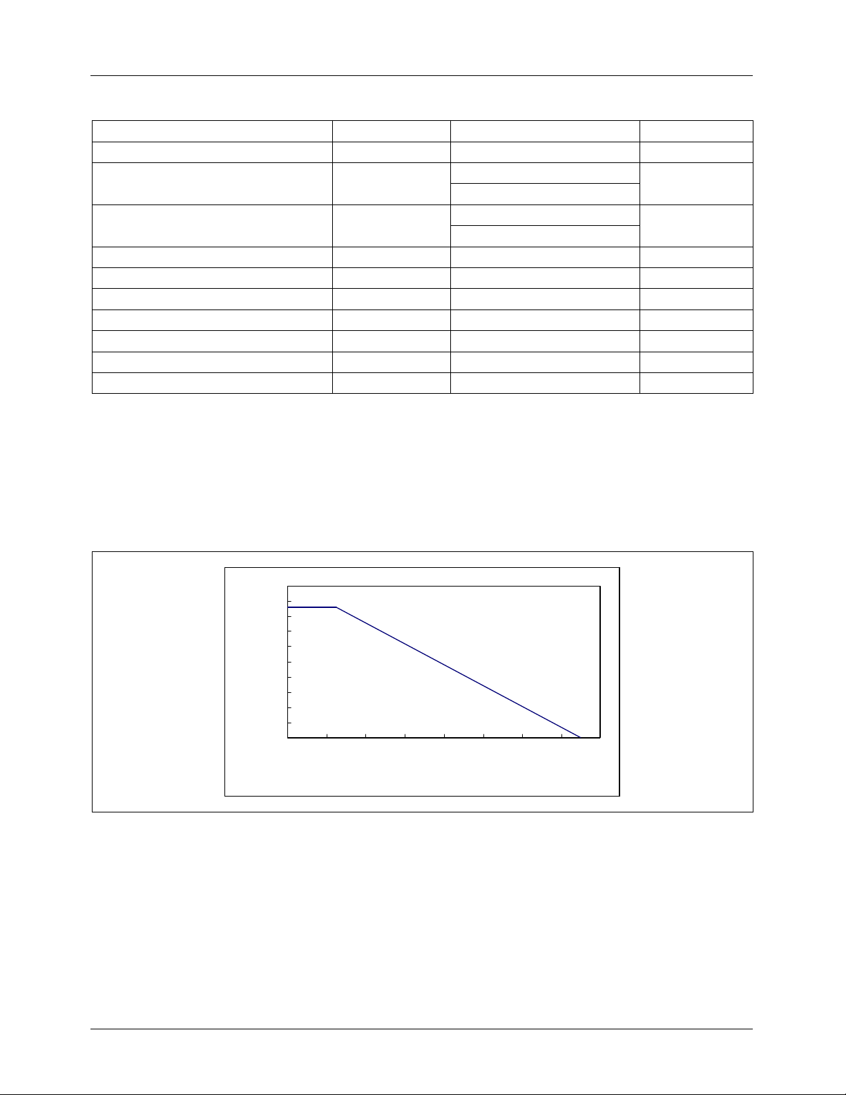
Power Dissipation Curve (Air condition = 0m/s)
0.5
0.45
0.4
0.35
0.3
0.25
Pd[W]
0.2
0.15
0.1
0.05
0
0 20 40 60 80 100 120 140 160
Tc or Ta[°C]
4
Page 5

FAN8408D
Air Speed & Θ
JA
350
300
250
200
150
JA[°C/W]
100
50
0
0123456
Air Speed[m/s]
Recommended Operating Conditions (Ta = 25°C)
Parameter Symbol Min. Typ. Max. Unit
Function compensation operating voltage V
CC
4.0 − 15.0 V
Electrical Characteristics
(Ta=25°C, VCC=12V unless otherwise specified)
Parameter Symbol Conditions Min. Typ. Max. Unit
Supply current I
Lock detector charging current I
Lock detector discharging current I
Lock detector charging/discharging ratio R
Lock detector capacitor clamp voltage V
Lock detector capacitor comparator voltage V
Output low level voltage V
Output leakage current I
Output zener voltage V
Hall output pin low level voltage V
Hall output pin leakage current I
Hall input dc range V
Hall input offset V
CC
LDC
LDD
CD
LDCL
LDCP
OL
OL
OZ
HLL
HLL
HDC
HOF
When output is off. - - 3.0 mA
VLD=1.8V 2.38 3.40 4.42 µA
VLD=1.8V 0.48 0.68 0.88 µA
RCD=I
LDC/ILDD
3.0 5.0 7.0 −
- 2.4 2.85 3.3 V
- 0.7 0.99 1.2 V
IO=200mA - 0.9 1.2 V
--010µA
Clamp current=10mA 28 30 32 V
IO=10mA - 0.2 0.5 V
--010µA
-
V
-1-
V
=6V -10 - 10 mV
REF
CC
2V
V
5
Page 6

FAN8408D
Application Information
1. Lock Detection & Automatic Restart
Hall Input
Output
V
LDCL
V
LDCP
Motor lock
detected
Motor lock
T
OFF
T
ON
Motor lock
cleared
Motor restart
FAN8408D features a lock detection and an automatic restart. The functions can be operated as follow s.
1) When the hall signal stop switching, a motor can be locked.
2) The voltage, V
on pin 3, is increasing until it reaches V
LD
LDCL
.
3) If LD pin is connected to GND, the lockup protection is disabled.
4) While a motor is locked, the output repeats switching ON / OFF , but the other output is always OFF. The switching time can
be determined by an external capacitor on charging / discharging time of the capacitor, switching ON / OFF time can be
calculated as follows.
T
T
ON
OFF
C
LDVLDCLVLDCP
------------------------------------------------------------------------ -=
C
LDVLDCLVLDCP
------------------------------------------------------------------------ -=
I
LDC
I
LDD
–()×
–()×
Where, The C
The V
LDCL
The V
LDCP
The I
LDC
The I
LDD
is an external capacitor connected to pin 3, LD.
LD
is the clamp voltage on pin 3, LD.
is the comparator voltage on pin 3, LD.
is the charging current on pin 3, LD.
is the dischaging current on pin 3, LD.
2. Thermal Shut Down
TSD On: All the outputs are off.(Typ. 175°C)
TSD Off: The circuit can be reactivated and begin to operate in a normal condition. (Typ. 150°C)
6
Page 7

3. Hall Amplifier Input Block
FAN8408D
V
CC
R1
FAN8408D
The hall current (IH) is determined by R1, R2 and R3.
V
I
H
CC
----------------------------------- -=
R1 R2 R3++
IN+
C1
5
C2
6
IN-
R2
Hall
Sensor
R3
Where, the R2 is the impedance of hall sensor.
An external capacitor, C1, can be used to reduce a power supply noise. In addition, C2 is to remove a noise which is caused in
case the line is long from the hall sensor output to the hall input (pin 5 / 6) of the device.
The input bias voltage of hall amplifier is between 1V and V
V
CC
-2V as following figure.
CC
VCC-2V
/ 2
V
CC
1V
GND
It is recommended that R1 and R3 should have the same value to make the output signal of hall sensor centered as V
CC
/2.
7
Page 8

FAN8408D
Operation Truth Ta ble
IN+ IN- OUT
A
OUT
B
High Low High Low Low
Low High Low High High
Test Circuits
V
CC
1K
50
OUT
1
2
B
HO
GND
OUT
HO
A
50
8
7
I
LDC
/ I
A
LDD
V
LD
3
LD
4
V
CC
IN-
IN+
6
5
A
I
CC
V
CC
8
Page 9

Typical Application Circuits
1
OUT
B
7
OUT
A
V
CC
4
8
GND
Commutation &
Control
& TSD
FAN8408D
LD
3
2
HO
V
CC
IN+
5
Hall
6
IN-
Precaution
In case of improper connection (change between power and ground), diode is required to protect motor.
9
Page 10

FAN8408D
Package Dimensions (Unit: mm)
8-SOP-225
10
Page 11

FAN8408D
11
Page 12

FAN8408D
DISCLAIMER
FAIRCHILD SEMICONDUCTOR RESERVES THE RIGHT TO MAKE CHANGES WITHOUT FURTHE R NOTICE TO ANY
PRODUCTS HEREI N TO IMPROVE RELIABILITY, FUNCTION OR DESIGN. FAIRCHIL D DOES NOT ASSUME AN Y
LIABILITY ARISING OUT OF THE APPLICATION OR USE OF ANY PRODUCT OR CIRCUIT DESCRIBED HEREIN; NEITHER
DOES IT CONVEY ANY LICENSE UNDER ITS PATENT RIGHTS, NOR THE RIGHTS OF OTHERS.
LIFE SUPPORT POL I CY
FAIRCHILD’S PRODUCTS ARE NOT AUTH ORIZED FOR USE AS CRI TICAL COMPONENTS IN LIFE SUPPORT DEVICES
OR SYSTEMS WITHOUT THE EXPRESS WRITTEN APPROVAL OF THE PRESIDENT OF FAIRCHILD SEMICONDUCTOR
CORPORATION. As used herein :
1. Life support devices or systems are devices or systems
which, (a) are intended for surgical implant into the body,
or (b) support or sustain life, and (c) whose failure to
perform when properly used in accordance with
2. A critical component in any component of a life support
device or system whose fa ilure to perform can be
reasonably expec ted to cause the failur e of the life support
device or system, or to affect its safety or effec t iv ene ss .
instructions for use provided in the labeling, can be
reasonably expected to result in a significant injury of the
user.
www.fairchildsemi.com
10/17/02 0.0m 001
2002 Fairchild Semiconductor Corporation
Stock#DSxxxxxxxx
 Loading...