

Page 1

©2001 Fairchild Semiconductor Corporation
www.fairchildsemi.com
Rev.1.0.1
Features
• 3-Phase BLDC motor driver IC with speed control
• Phase Locked Loop (PLL) speed control
• Built-in phase locked detector output
• Current linear drive scheme
• External clock for arbitrary motor speed
• Built-in FG amplifier and integrating amplifier
• Auto Gain Control (AGC) circui t for compensation hall
amplifier
• Built-in protection circuits (over-current limit, under
voltage limit, thermal shut down)
Description
The FAN8400D is a monolithic integrated circuit. it is one
driver for laser beam printe r (LBP) polygon mirror motor,
which has single chip implementation of all circuits. For
extremely high rotational precision, it employs the phase
locked loop (PLL) speed control scheme.
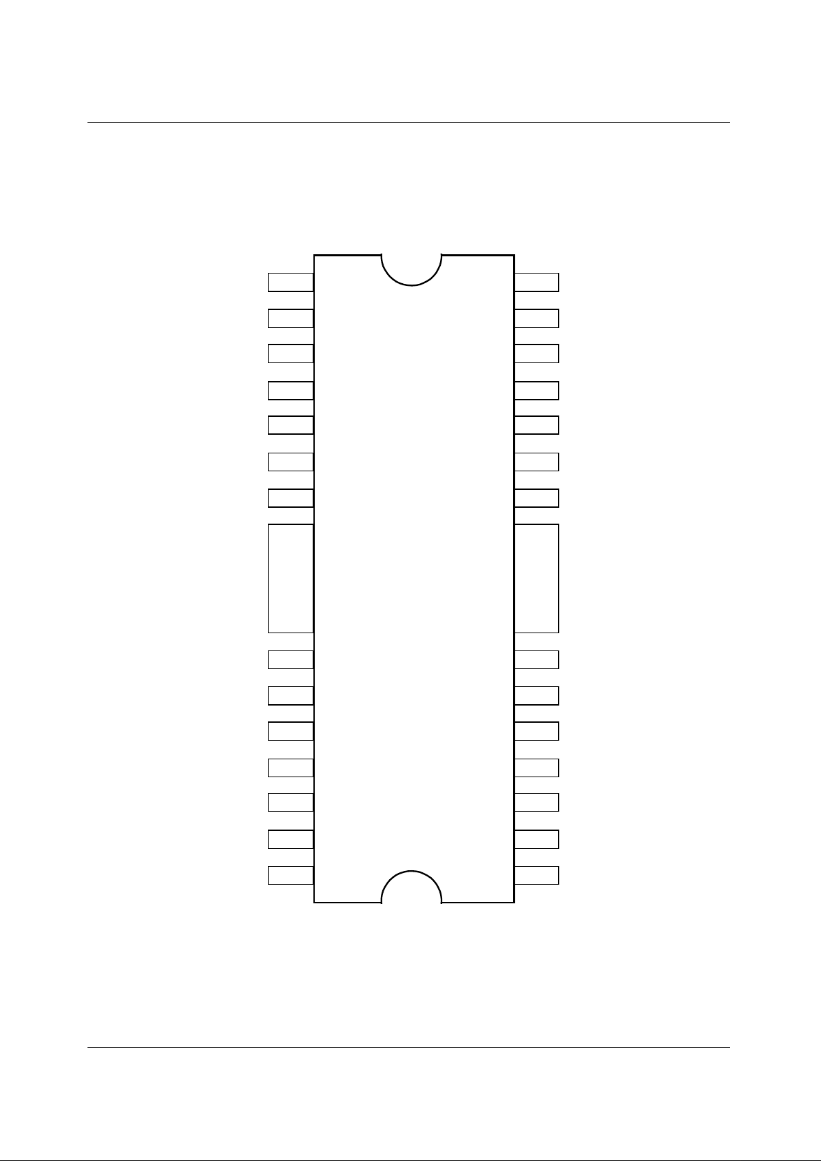
28-SSOPH-375SG2
Typical application
• Polygon mirror motor drive IC for laser beam printer
• Polygon mirror motor drive IC for facsimile
• Polygon mirror motor drive IC for duplicator
• Polygon mirror motor driv e IC for multi function printer
• General 3 phase BLDC motor drive IC
Ordering Information
Device Package Operating Temp
FAN8400BD3 28-SSOPH-375SG2 −20°C ~ +80°C
FAN8400BD3TF 28-SSOPH-375SG2 −20°C ~ +80°C
FAN8400D (FAN8400BD3)
3-Phase BLDC Motor Driver with PLL
Page 2
FAN8400D (FAN8400BD3)
2
Pin Assignments
AGC
FIN
1
2
3
4
5
6
7
8
9
10
11
12
13
14
FIN
28
27
26
25
24
23
22
21
20
19
18
17
16
15
FG
IN-
FG
S
FG
OUT
S/S
NC
SGND
LD
ECLK
PD
E
I
E
O
F
C
NC
V
REG
V
CC
PGND
R
F
U
V
W
H
V+
H
V-
H
U+
H
U-
H
W+
H
W-
FAN8400D
NC
Page 3

FAN8400D (FAN8400BD3)
3
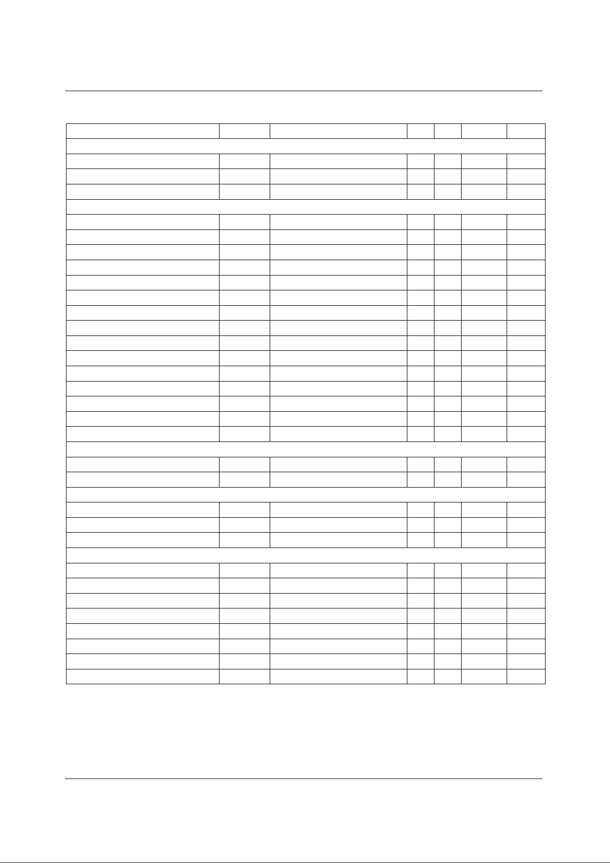
Pin Definitions
Pin Number Pin Name Pin Function Description
1 AGC AGC amplifier frequency characteristics correction
2FG
IN-
FG amplifier inverting input
3FG
S
FG pulse output
4FG
OUT
FG amplifier output
5 S/S Stop and start
6NC 7NC 8 SGND Signal ground
9 LD Phase locked loop detector output
10 ECLK External clock
11 PD Phase locked loop detector output
12 E
I
Error amplifier inverting input
13 E
O
Error amplifier output
14 F
C
Control amplifier frequency correction
15 NC 16 V
REG
Regulator voltage stabilization output
17 V
CC
Power supply
18 PGND Power ground
19 R
F
Output current detection
20 U U output
21 V V output
22 W W output
23 H
V+
V hall amplifier non inverting input
24 H
V-
V hall amplifier inverting input
25 H
U+
U hall amplifier non inverting input
26 H
U-
U hall amplifier inverting input
27 H
W+
W hall amplifier non inverting input
28 H
W-
W hall amplifier inverting input
Page 4

FAN8400D (FAN8400BD3)
4
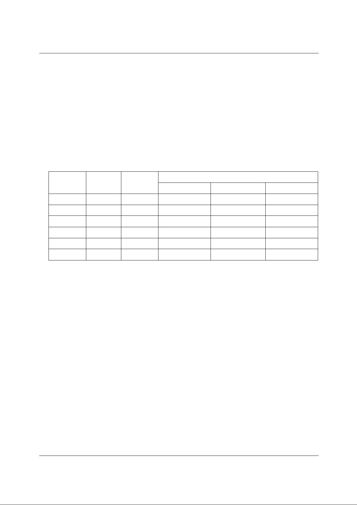
Internal Block Diagram
AGC
FIN
1
2
3
4
5
6
7
8
9
10
11
12
13
14
FIN
28
27
26
25
24
23
22
21
20
19
18
17
16
15
FG
IN-
FG
S
FG
OUT
S/S
NC
SGND
LD
ECLK
PD
E
I
E
O
F
C
NC
V
REG
V
CC
PGND
R
F
U
V
W
H
V+
H
V-
H
U+
H
U-
H
W+
H
W-
V
REG
2
V
REG
2
Regulator
Output
Controller
Hall
AMP
Matrix
AGC
Clock
PLL
Lock
Detector
TSD &
UVLO
-
+
S/S
-
+
-
+
OCL
V-type
Control
NC
Page 5

FAN8400D (FAN8400BD3)
5
Absolute Maximum Ratings (Ta = 25°°°°C)
Recommended Operating Conditions (Ta = 25°°°°C)
Parameter Symbol Value Unit Remark
Maximum supply voltage V
CCMAX
30 V -
Maximum output current I
OMAX
0.6 A Power dissipation Pd 1.7 W Operating temperature T
OPR
−20 ~ +80 °C-
Storage temperature T
STG
−50 ~ +150 °C-
Parameter Symbol Min. Typ. Max. Unit
Operating voltage range V
CC
20 24 28 V
Page 6
FAN8400D (FAN8400BD3)
6
Electrical Characteristics (Ta = 25°°°°C)
Parameter Symbol Conditions Min. Typ. Max. Unit
POWER SUPPLY CURRENT
Low power supply current I
CCL
Stop mode, VCC=20V 20 30 40 mA
Typical power supply current I
CCT
Stop mode, VCC=24V 21 31 41 mA
High power supply current I
CCH
Stop mode, VCC=28V 22 32 42 mA
OUTPUT POWER TRANSISTOR CHARACTERISTICS (V
AGC
= 3.5V)
U source saturation voltage (1) V
SATUU1IO
=0.6A, RF=0Ω -1.8 2.5 V
U source saturation voltage (2) V
SATUU2IO
=0.3A, RF=0Ω -1.6 2.3 V
U sink saturation voltage (1) V
SATUL1IO
=0.6A, RF=0Ω -0.5 1.0 V
U sink saturation voltage (2) V
SATUL2IO
=0.3A, RF=0Ω -0.25 0.7 V
V source saturation voltage (1) V
SATVU1IO
=0.6A, RF=0Ω -1.8 2.5 V
V source saturation voltage (2) V
SATVU2IO
=0.3A, RF=0Ω -1.6 2.3 V
V sink saturation voltage (1) V
SATVL1IO
=0.6A, RF=0Ω -0.5 1.0 V
V sink saturation voltage (2) V
SATVL2IO
=0.3A, RF=0Ω -0.25 0.7 V
W source saturation voltage (1) V
SATWU1IO
=0.6A, RF=0Ω -1.8 2.5 V
W source saturation voltage (2) V
SATWU2IO
=0.3A, RF=0Ω -1.6 2.3 V
W sink saturation voltage (1) V
SATWL1IO
=0.6A, RF=0Ω -0.5 1.0 V
W sink saturation voltage (2) V
SATWL2IO
=0.3A, RF=0Ω -0.25 0.7 V
U output leakage current I
OLEAKUVCC
=28V, U=28V - - 100 µA
V output leakage current I
OLEAKVVCC
=28V, V=28V - - 100 µA
W output leakage current I
OLEAKWVCC
=28V, W=28V - - 100 µA
UNDER VOLTAGE LIMIT
UVLO operating voltage V
SD
- 7.0 7.6 8.2 V
UVLO hysteresis HV
SD
- 1.0 1.3 1.6 V
REGULATOR VOLTAGE OUTPUT
Regulator output voltage V
REG
- 5.8 6.3 6.8 V
Power supply variation H
VREG1VCC
=20~28V - - 100 mV
Load variation H
VREG2ILOAD
=0~10mA - - 100 mV
HALL AMPLIFIER INPUT BLOCK
H
U+
hall AMP input bias current I
BHA1+
--210µA
H
U−
hall AMP input bias current I
BHA1−
--210µA
H
V+
hall AMP input bias current I
BHA2+
--210µA
H
V−
hall AMP input bias current I
BHA2−
--210µA
H
W+
hall AMP input bias current I
BHA3+
--210µA
H
W−
hall AMP input bias current I
BHA3−
--210µA
Hall differential input range V
HIN
Sine wave input 50 - 350 mVp-p
Hall common input range V
ICM
Differential input : 50mVp-p 3.5 - VCC-3.5 V
Page 7

FAN8400D (FAN8400BD3)
7
Electrical Characteristics (Continued)
Parameter Symbol Conditions Min. Typ. Max. Unit
FG AMPLIFIER BLOCK
FG AMP. input bias current I
BFG
--1-1µA
FG AMP. DC bias level V
BFG
- 2.90 3.15 3.40 V
FG output high level voltage V
OHFG
No external load V
REG
-1.1V - - V
FG output low level voltage V
OLFG
No external load - 0.8 1.2 V
FG SCHMIDT COMPARATOR BLOCK
FGS high / low input hysteresis V
SHL
--50050mV
FGS low / high input hysteresis V
SLH
- 100 150 200 mV
FGS hysteresis V
FGL
- 100 - 200 mV
FGS input operating level V
FGSIL
- 400 - - mVp-p
FGS output saturation voltage V
FGSSATIFGS
=4mA - 0.2 0.4 V
FGS output leakage current I
FGSLEAKVCC
=28V - - 10 µA
ERROR AMPLIFIER BLOCK
Error AMP. input bias current I
BER
--1-1µA
Error AMP. DC bias level V
BER
- 2.90 3.15 3.40 V
Error output high level voltage V
OHER
No external load V
REG
-1.1V - - V
Error output low level voltage V
OLER
No external load - - 1.0 V
CURRENT LIMIT OPERATION
R
F
output voltage limit V
RF
- 0.55 0.60 0.65 V
CONTROLLER BLOCK
Dead zone V
DZ
- 50 100 300 mV
Output idle voltage V
ID
---5mV
Forward gain G
DF+
-0.40.50.6-
Reverse gain G
DF−
- -0.6 -0.5 -0.4 -
Accelerate command voltage V
STA
-V
REG
-1.1V - - V
Decelerate command voltage V
STO
--0.81.5V
Forward limit voltage V
L+
RF=22Ω -0.60-V
Reverse limit voltage V
L−
RF=22Ω -0.60-V
PHASE COMPARATOR OUTPUT BLOCK
PD output high level voltage V
PDH
No external load 5.2 - - V
PD output low level voltage V
PDL
No external load - - 0.7 V
PD output source current I
PD+
VPD=0.5*V
REG
---0.6mA
PD output sink current I
PD−
VPD=0.5*V
REG
1.0 - - mA
PHASE LOCKED LOOP DETECTOR OUTPUT BLOCK
LD output saturation voltage V
LDSATILD
=5mA - 0.1 0.4 V
LD output leakage current I
LDLEAKVCC
=28V - - 10 µA
Page 8

FAN8400D (FAN8400BD3)
8
Electrical Characteristics (Continued)
Parameter Symbol Conditions Min. Typ. Max. Unit
EXTERNAL CLOCK INPUT BLOCK
External input frequency F
CLK
External clock mode 0.5 - 7.0 KHz
ECLK input open voltage V
IOCLK
- 3.7 4.2 4.7 V
ECLK input high level current I
IHCLK
V
CLK=VREG
100 150 200 µA
ECLK input low level current I
ILCLK
V
CLK
=0V -400 -300 -200 µA
S/S BLOCK
S/S input high level voltage V
IHSS
-3.0-V
REG
V
S/S input low level voltage V
ILSS
-0-1.5V
S/S hysteresis V
ISSS
- 0.3 0.5 0.7 V
S/S input open voltage VIOSS - 3.7 4.2 4.7 V
S/S input high level current I
IHSS
VSS=V
REG
100 150 200 µA
S/S input low level current I
ILSS
VSS=0V -400 -300 -200 µA
Page 9
FAN8400D (FAN8400BD3)
9
Application Information
1. Output Block
• 3 Phase power transistor and free wheeling diodes
• Reverse active type upper side diodes and parasitic lower side diodes
• full wave current linear drive with current feedback
• Connection with external capacitor to prevent voltage spike and oscillation by current drive
• Output transistor commutation by "Winner takes all" method
• Built in over current limit (OCL) circuit
2. Hall AMP Block
• Detection of rotor position using 3 phase hall sensors
• Determination of output commutation by hall signal
3. AGC Block
• This block is remained output amplitude.
• It is controlled by envelope through hall signals.
NOTES:
V
AGC
is voltage of AGC output.
H
NI
is hall non inverting input voltage.
H
I
is hall inverting voltage.
4. Speed Control Block
• Digital phase locked loop (PLL) circuit
• Generating error pulse between rising edge of clock and falling edge of FG signal.
• High precision stable speed control
Hall U Hall V Hall W
Forward torque [ Reverse torque]
Output U Output V Output W
H L H L [H] H [L] M [M]
H L L L [H] M [M] H [L]
H H L M [M] L [M] H [L]
L H L H [L] L [H] M [M]
L H H H [L] M [M] L [H]
L L H M [M] H [L] L [H]
V
AGC
1
H
NIHI
–
-------------------- -
∝
Page 10

FAN8400D (FAN8400BD3)
10
5. FG AMP & FG Schmidt Comparator Block
• This block measures of motor rotation speed and controls motor speed.
• It is determined FG AMP gain and filter by external component.
• FG schmidt block change sine wave form to square wave form
6. Error AMP Block
• It composes of dumping filter and ripple filter by external component.
• It determines output amplitude of error AMP by width error pulse.
• It is determined output current by output amplitude of error AMP.
• Bidirectional torque control
7. Regulator Block
• Power supply of control circuits in inside.
• Band gap reference circuits.
8. Lock Detector
• It is low when FG frequency reaches capture range of clock frequency.
• Open correct
9. FG Pulse Output
• Monitoring pin for motor rotative speed
• Open correct
10. Stop And Start
• Stop mode: O pen or high voltage
• Start mode: Low voltage
V
DZ
Reverse
Direction
Forward
Direction
V
RF
V
EO
V
REG
/2
Page 11
FAN8400D (FAN8400BD3)
11
Test Circuits
3.5V
+
0.1u
V
CC
56K
1K
1K
V
CC
10K
VREG
+
0.1u
H
W
+
H
U
+
H
V
+
+
0.1u
V
CC
+
10u
22
V
CC
V
CC
V
CC
1
2
3
4
5
6
7
8
9
10
11
12
13
14
28
27
26
25
24
23
22
21
20
19
18
17
16
15
FAN8400D
Page 12

FAN8400D (FAN8400BD3)
12
Typical Application Circuits
H
W
-
+
H
U
-
+
H
V
-
+
V
CC
+
1
2
3
4
5
6
7
8
9
10
11
12
13
14
28
27
26
25
24
23
22
21
20
19
18
17
16
15
FAN8400D
M
S/S
FG
S
FG
Sensor
LD
ECLK
Page 13

FAN8400D (FAN8400BD3)
13
Page 14

FAN8400D (FAN8400BD3)
11/7/01 0.0m 001
Stock#DSxxxxxxxx
2001 Fairchild Semiconductor Corporation
LIFE SUPPORT POL I CY
FAIRCHILD’S PRODUCTS ARE NOT AUTHORIZED FOR USE AS CRITICAL COMPONENTS IN LIFE SUPPORT DEVICES
OR SYSTEMS WITHOUT THE EXPRESS WRITTEN APPROVAL OF THE PRESIDENT OF FAIRCHILD SEMICONDUCTOR
CORPORATION. As used herein :
1. Life support devices or systems are devices or systems
which, (a) are intended for surgical implant into the body,
or (b) support or sustain life, and (c) whose failure to
perform when properly used in accordance with
instructions for use provided in the labeling, can be
reasonably expected to result in a significant injury of the
user.
2. A critical component in any component of a life support
device or sys tem whose failure to perform can be
reasonably expec ted to cause the failur e of the life support
device or system, or to affect its safety or effec tiveness.
www.fairchildsemi.com
DISCLAIMER
FAIRCHILD SEMICONDUCTOR RESERVES THE RIGHT TO MAKE CHANGES WITHOUT FURTHER NOTICE TO ANY
PRODUCTS HEREI N TO IMPROVE RELIABILITY, FUNCTION OR DES IGN. FAIRCHILD DOES NOT ASSUME ANY
LIABILITY ARISING OUT OF THE APPLICATION OR USE OF ANY PRODUCT OR CIRCUIT DESCRIBED HEREIN; NEITHER
DOES IT CONVEY ANY LICENSE UNDER ITS PATENT RIGHTS, NOR THE RI GHTS OF OTHERS.
 Loading...