

Page 1

www.fairchildsemi.com
FAN8200/FAN8200D/FAN8200MTC
FAN8200MP
Low Voltage/Low Saturation Stepping Motor Driver
Features
• 3.3V and 5V MPU interface
• Dual H-bridge drivers for bipolar stepping motor drives
• Built-in vertical-PNP power transistors
• Wide supply voltage range (V
• Low saturation voltage (0.4V@ 0.4A)
• Built-in chip enable function for each bridge
• Built-in shoot-through current protection
• Built-in thermal shutdown(TSD) function
= 2.5V ~ 7.0V)
CC
Description
The FAN8200/FAN8200D/FAN8200MTC/FAN8200MP is a
monolithic intergrated circuit designed for two-phase stepping motor drive systems. It has dual H-bridge drivers with
vertical-PNP power transistors. Each of the bridges has an
independant enable pin, therefore it can be used for other
applications as well as stepping motor drive systems.
14-DIP-300
1
14-SOP-225
1
14-TSSOP
1
14-MLP
Typical Application
• General low voltage stepping motor driver
• Floppy disk driver
• Camera stepping motor driver
• PC camera or security equipment motion controller
• Two channel DC motor driver for a digital still camera
(DSC)
• MPU interfaced general power driver (buffer)
©2003 Fairchild Semiconductor Corporation
Ordering Information
Device Package Operating Temp.
FAN8200 14-DIP-300 -20 ~ +75°C
FAN8200D 14-SOP-225 -20 ~ +75°C
FAN8200DTF 14-SOP-225 -20 ~ +75°C
FAN8200MTC 14-TSSOP -20 ~ +75°C
FAN8200MTCX 14-TSSOP -20 ~ +75°C
FAN8200MP
FAN8200MPX
14-MLP -30 ~ +80°C
Rev. 1.0.4
Page 2

FAN8200/FAN8200D/FAN8200MTC FAN8200MP
Pin Assignments
PGND
CE2
OUT3
VS2
OUT4
1011121314
IN2
PGND
98
FAN8200/FAN8200D/
8200MTC/8200MP
1234567
V
CC
CE1
OUT1
VS1
OUT2
IN1
SGND
Pin Definitions
Pin Number Pin Name I/O Pin Function Description
1V
CC
2 CE1 I Chip enable 1
3 OUT1 O Output 1
4 VS1 - Power supply 1
5 OUT2 O Output 2
6 IN1 I Input 1
7 SGND - Signal ground
8 PGND - Power ground
9 IN2 I Input 2
10 OUT4 O Output 4
11 VS2 - Power supply 2
12 OUT3 O Output 3
13 CE2 I Chip enable 2
14 PGND - Power ground
- Logic part supply voltage
2
Page 3

Internal Block Diagram
V
1
CC
FAN8200/FAN8200D/FAN8200MTC FAN8200MP
4
VS1
3
OUT1
IN1
CE1
SGND
IN2
CE2
50K
6
80K
50K
2
80K
7
50K
9
80K
50K
13
80K
Control
Part1
Control
Part2
TSD &
BIAS
5
OUT2
8
PGND
11
VS2
12
OUT3
10
OUT4
14
PGND
3
Page 4
FAN8200/FAN8200D/FAN8200MTC FAN8200MP
Absolute Maximum Ratings (Ta = 25°C)
Parameter Symbol Value Unit
Supply voltage V
Power supply voltage V
Output voltage V
Input voltage V
Peak output current per channel I
Continuous output current per channel I
Power dissipation P
Junction temperture T
Storage temperature T
Operating temperature T
Notes:
1. When mounted on 76.2mm
2. Power dissipation reduces 8.0mW/
FAN8200MP for Ta ≥ 25°C.
3. Should not exceed P
× 114mm × 1.57mm PCB (glass epoxy material).
°C for FAN8200, 4.8mW/°C for FAN8200D, 6.9mW/°C for FAN8200MTC and 6.4mW/°C
and SOA(Safe Operating Area).
D
CC(MAX)
S(MAX)
OUT(MAX)
IN(MAX)
O(PEAK)
O
note
D
J
STG
A
0.65 (FAN8200)
0.4 (FAN8200D)
0.55 (FAN8200MTC)
0.35 (FAN8200MP)
1.0 (FAN8200)
0.6 (FAN8200D)
0.87 (FAN8200MTC)
0.8 (FAN8200MP)
-20 ~ 75(FAN8200)
-20 ~ 75(FAN8200D)
-20 ~ 75(FAN8200MTC)
-30 ~ 80(FAN8200MP)
9.0 V
9.0 V
VS + V
CF
7.0 V
1A
150 °C
-40 ~ 125 °C
V
A
W
°C
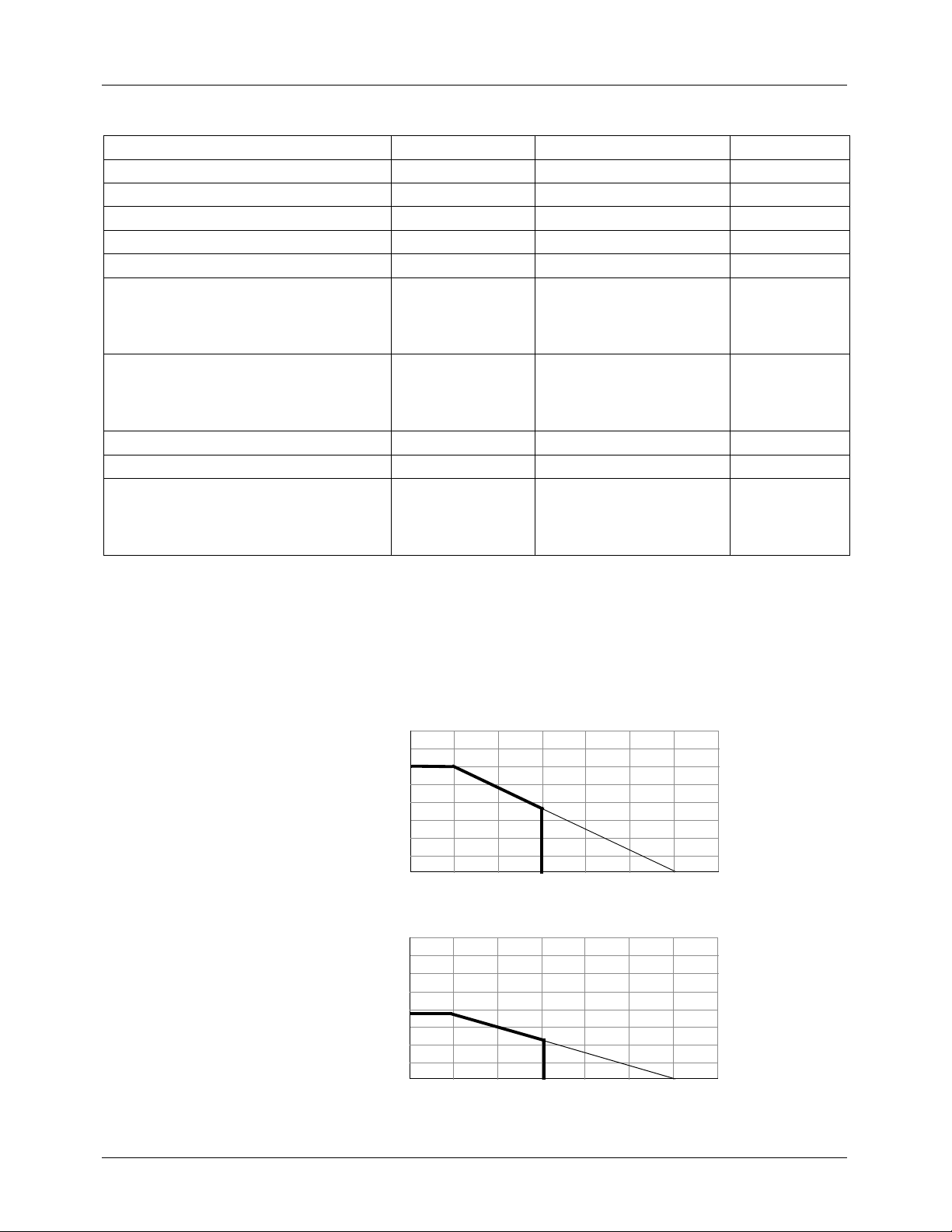
Power Dissipation Curve
Power
Dissipation
FAN8200
FAN8200D
: PD[W]
Power
Dissipation
: PD[W]
1.0
0.5
1.0
0.6
SOA
0
0255075100125
Ambient temperature, Ta [°C]
SOA
0
0255075100125
Ambient temperature, Ta [°C]
150 175
150 175
4
Page 5
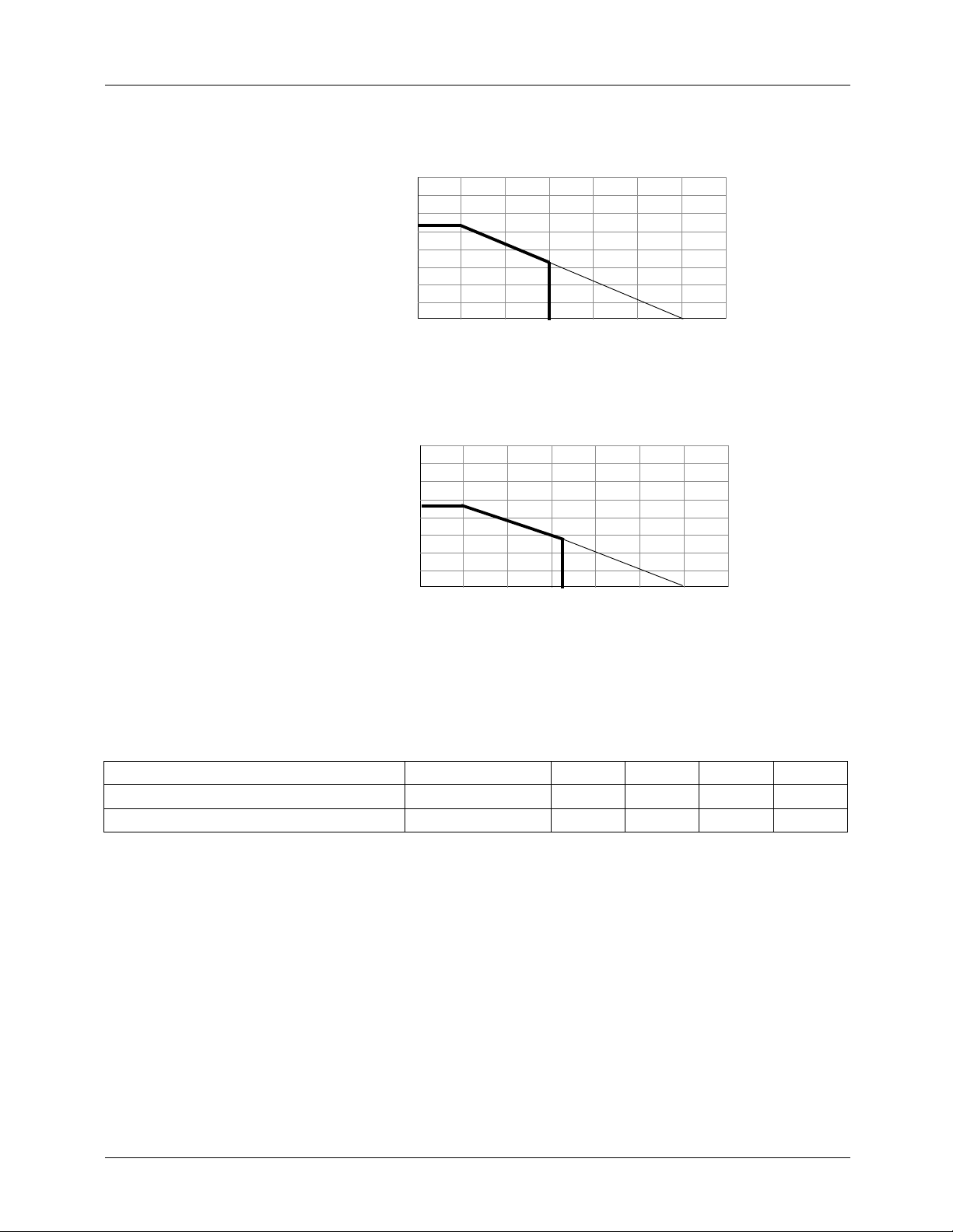
Power Dissipation Curve (Continued)
FAN8200/FAN8200D/FAN8200MTC FAN8200MP
FAN8200MTC
FAN8200MP
Power
Dissipation
: PD[W]
Power
Dissipation
: PD[W]
1.0
0.5
1.0
0.5
SOA
0
0255075100125
Ambient temperature, Ta [°C]
SOA
0
0255075100125
Ambient temperature, Ta [°C]
150 175
150 175
Recommended Operating Conditions (Ta = 25°C)
Parameter Symbol Min. Typ. Max Unit
Logic circuit supply voltage V
Power supply voltage V
CC
S
2.5 - 7.0 V
2.5 - 7.0 V
5
Page 6

FAN8200/FAN8200D/FAN8200MTC FAN8200MP
Function Descriptions
CE1 IN1 OUT1 OUT2 CE2 IN2 OUT3 OUT4
Low X Z Z Low X Z Z
High Low High Low High Low High Low
High High Low High High High Low High
X: don’t care
Z: high-impedance
CE1
CE2
IN1
IN2
Phase-A
OUT1-OUT2
Phase-B
OUT3-OUT4
+VS
-VS
High-ImpedanceHigh-Impedance
+VS
-VS
6
Page 7

FAN8200/FAN8200D/FAN8200MTC FAN8200MP
Electrical Characteristics
(Ta=25°C, VCC=5V, VS1=3V, VS2=3V, unless otherwise specified)
Parameter Symbol Conditions Min. Typ. Max. Unit
Supply current 1 I
Supply current 2 I
Saturation voltage 1
(upper + lower total)
Saturation voltage 2
(upper + lower total)
V
V
Input high level voltage V
Input low level voltage V
Input current I
Chip enable current I
Clamp diode leakge current I
Clamp diode voltage V
CC1
CC2
SAT1
SAT2
INH
INL
IN
CE
LEAK
CF
CE1, 2=0V - 0.1 10 uA
CE1=3V, CE2=0V
or CE1=0V, CE2=3V
CE1=3V, IN1=3V
or 0V, I
OUT
=0.2A
CE1=3V, IN1=3V
or 0V, I
OUT
=0.4A
-1.8-V
-1218mA
-0.20.3 V
-0.40.6 V
CC
- -0.3 - 0.7 V
IN=3V, Each pin - 100 200 uA
CE=3V, Each pin - 100 200 uA
VCC=7V, VS=7V - - 30 uA
I
=0.4A - - 1.7 V
OUT
Typical Performance Characteristics
V
V
SAT
vs. I
Characteristics Graph
OUT
V
V
SAT
SAT
V
[V]
[V]
[V]
SAT
1.0
1.0
0.8
0.8
0.6
0.6
0.4
0.4
0.2
0.2
0
0
0 100 200 300 400 500 600 700
0 100 200 300 400 500 600 700
I
I
[A]
[A]
O
O
[A]
I
OUT
7
Page 8

FAN8200/FAN8200D/FAN8200MTC FAN8200MP
Test Circuits
V
CC
V
CC
IN1
CE1
1
6
2
0.1uF
Control
Part1
SW1
SW2
VS1
4
OUT1
3
OUT2
5
SW4
SW5
15Ω6Ω
SW3
SGND
IN2
CE2
PGND
7
TSD &
BIAS
9
Control
Part2
13
8
VS2
11
OUT3
12
OUT4
10
PGND
14
SW6
6Ω
SW7
15Ω
8
Page 9

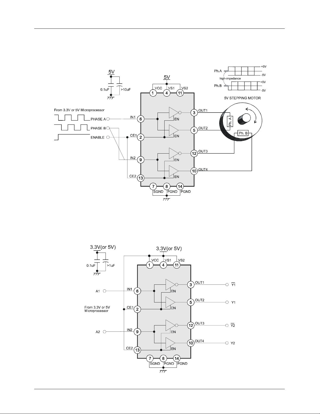
Typical Application Circuit
V
CC
V
CC
1
IN1
6
CE1
2
SGND
7
0.1uF
Control
Part1
TSD &
BIAS
FAN8200/FAN8200D/FAN8200MTC FAN8200MP
VS1
4
OUT1
3
OUT2
5
PGND
8
Stepping
Motor
VS2
11
From
3.3V or 5V
Microprocessor
IN2
CE2
OUT3
12
9
Control
Part2
13
OUT4
10
PGND
14
9
Page 10
FAN8200/FAN8200D/FAN8200MTC FAN8200MP
Application Example - Full Step Bipolar Drive
Circuit Schematics
FAN8200/D/MTC
Application Example - Large Current Buffer
Circuit Schematics
FAN8200/D/MTC
10
Page 11

FAN8200/FAN8200D/FAN8200MTC FAN8200MP
Application Example - 2-Ch. dc Motor Driver for a Digital Still Camera(DSC)
Circuit Schematics
Shutter
direction
Shutter
enable
Iris
direction
Iris
enable
FAN8200/D/MTC
IN1=high
IN2=high
Shutter
dc motor
M
M
Iris
dc motor
IN1=low
IN2=low
11
Page 12

FAN8200/FAN8200D/FAN8200MTC FAN8200MP
#
#
)
Mechanical Dimensions (Unit: mm)
Package Dimensions
14-DIP-300
6.40 ±0.20
±0.008
0.252
2.08
(
0.082
1
7
7.62
0.300
#14
#8
MAX
19.80
0.780
3.25 ±0.20
0.128 ±0.008
19.40 ±0.20
0.764 ±0.008
0.46 ±0.10
0.20
0.008
0.018 ±0.004
2.54
MIN
1.50 ±0.10
0.100
0.059 ±0.004
5.08
MAX
0.25
0.010
0.200
+0.10
–0.05
+0.004
–0.002
0~15°
12
3.30 ±0.30
0.130 ±0.012
Page 13

Mechanical Dimensions (Unit: mm) (Continued)
2
Package Dimensions
14-SOP-225
1.55 ±0.10
0.061 ±0.004
FAN8200/FAN8200D/FAN8200MTC FAN8200MP
0.05
MIN
0.00
0.47
0.019
()
0.10
+
0.20
-0.05
0.004
+
-0.002
0.008
#1
#7
6.00 ±0.30
0.236 ±0.012
3.95 ±0.20
0.156 ±0.008
#14
#8
MAX
8.70
0.343
1.80
0.071
8.56 ±0.20
MAX
0.337 ±0.008
MAX0.10
MAX0.004
+0.10
-0.05
0.406
0.004
+
1.27
-0.002
0.016
0.050
0.60 ±0.20
0.024 ±0.008
5.72
0.225
0~8°
13
Page 14

FAN8200/FAN8200D/FAN8200MTC FAN8200MP
Mechanical Dimensions (Unit: mm) (Continued)
Package dimensions
14-TSSOP
14
Page 15

Mechanical Dimensions (Unit: mm) (Continued)
Package dimensions
14-MLP
FAN8200/FAN8200D/FAN8200MTC FAN8200MP
15
Page 16

FAN8200/FAN8200D/FAN8200MTC FAN8200MP
DISCLAIMER
FAIRCHILD SEMICONDUCTOR RESERVES THE RIGHT TO MAKE CHANGES WITHOUT FURTHER NOTICE TO ANY
PRODUCTS HEREIN TO IMPROVE RELIABILITY, FUNCTION OR DESIGN. FAIRCHILD DOES NOT ASSUME ANY
LIABILITY ARISING OUT OF THE APPLICATION OR USE OF ANY PRODUCT OR CIRCUIT DESCRIBED HEREIN; NEITHER
DOES IT CONVEY ANY LICENSE UNDER ITS PATENT RIGHTS, NOR THE RIGHTS OF OTHERS.
LIFE SUPPORT POLICY
FAIRCHILD’S PRODUCTS ARE NOT AUTHORIZED FOR USE AS CRITICAL COMPONENTS IN LIFE SUPPORT DEVICES
OR SYSTEMS WITHOUT THE EXPRESS WRITTEN APPROVAL OF THE PRESIDENT OF FAIRCHILD SEMICONDUCTOR
CORPORATION. As used herein:
1. Life support devices or systems are devices or systems
which, (a) are intended for surgical implant into the body,
or (b) support or sustain life, and (c) whose failure to
perform when properly used in accordance with
2. A critical component in any component of a life support
device or system whose failure to perform can be
reasonably expected to cause the failure of the life support
device or system, or to affect its safety or effectiveness.
instructions for use provided in the labeling, can be
reasonably expected to result in a significant injury of the
user.
www.fairchildsemi.com
8/7/03 0.0m 001
2003 Fairchild Semiconductor Corporation
Stock#DSxxxxxxxx
 Loading...