

Page 1
FAN8038B(KA3038)
4-Channel Motor Drive IC
www.fairchildsemi.com
Features
• 4-CH H-Bridge Driver
• Built-in DC/DC Converter Controller Circuit
• Built-in Reset Circuit
• Built-in Battery Charging Circuit
• Built-in Voltage Drop Detector
• Built-in Thermal Shutdown Circuit
• Built-in General OP-AMP
• Low Power Consumption
• Built-in Power Controller Circuit
Description
FAN8038B is monolithic IC for portable CD play e r.
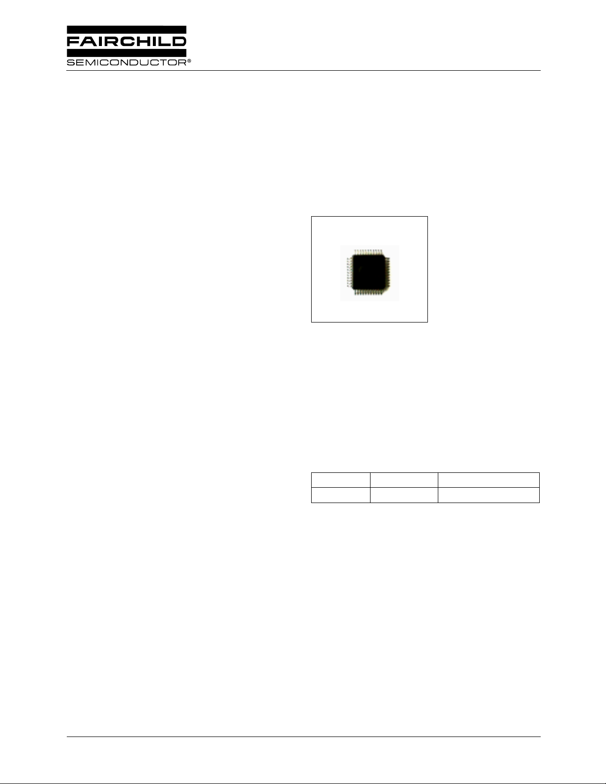
44-QFP-1010B
Typical application
• Portable Compact Disk Player (CDP)
• Portable Mini Disk Player (MD)
•Disc-Man
• Other Potable Compact Disk Media
©2002 Fairchild Semiconductor Corporation
Ordering Information
Device Package Operating Temp.
FAN8038B 44-QFP-1010B -35°C ~ +85°C
Rev. 1.0.3
Page 2

FAN8038B(KA3038)
Pin Assignments
OVP
BATT
RSTOUT
DEDSET
BDSW
ERRO
ERRI
SCP
COSC
34353637383940414243
RST
33
32
31
30
29
CHGSET
DO1(-)
DO1(+)
DO2(-)
DO2(+)
EMP
FIL SGND EMPSET ADPVCC STOP START CLKIN PWM
44
1
2
3
4
5
DVCC
FAN8038B
6
7
8
9
28
27
26
25
PGND
DO3(+)
DO3(-)
DO4(+)
NC
OPIN(-)
10
11
12 13 14 15 16 17 18 19 20 21 22
SVCC1 OPOUT OPIN(+) SVCC2 VREF DI3 DI4 MUTE34
24
DO4(-)
23
BRAKE
DI2
MUTE2
DI1
2
Page 3

Pin Definitions
Pin Number Pin Name Pin Function Description
1 OVP Battery Power Supply Mode
2 BATT Battery Power Supply
3 RSTOUT RSTOUT Detection Output
4 DEDSET DEDSET Time Setting
5 BDSW Booster Transistor Drive
6 ERRO Error Amp Output
7 ERRI Error Amp Input
8 SCP Short Circuit Protection Setting
9 COSC Triangular Wave Output
10 N.C No Connection
11 OPIN(-) OP-AMP Negative Input
12 SVCC1 Control Circuit Power Supply
13 OPOUT OP-AMP Output
14 OPIN(+) OP-AMP Positive Input
15 SVCC2 Pre-Drive Power Supply
16 VREF Reference Voltage
17 DI3 CH3 Control Signal Input
18 DI4 CH4 Control Signal Input
19 MUTE34 CH3, 4 Mute
20 DI2 CH2 Control Signal Input
21 MUTE2 CH2 Mute
22 DI1 CH1 Control Signal Input
23 BRAKE CH1 Brake
24 DO4(-) CH4 Negative Output
25 DO4(+) CH4 Positive Output
26 DO3(-) CH3 Negative Output
27 DO3(+) CH3 Positive Output
28 PGND Power Unit Power Ground
29 DO2(+) CH2 Positive Output
30 DO2(-) CH2 Negative Output
31 DO1(+) CH1 Positive Output
32 DO1(-) CH1 Negative Output
33 CHGSET Charge Current Setting
34 RST RSTOUT Inverting Output
35 EMP Empty Detection Output
36 DVCC H-Bridge Power Supply
37 PWM PWM Transistor Drive
38 CLKIN External Clock Input
39 START Boost DC/DC Converter Starting
40 STOP Boost DC/DC Converter Off
41 ADPVCC Charging Circuit Power Supply
42 EMPSET Empty Dection Level Converting
43 SGND Signal Ground
44 FIL PWM Phase Compensation
FAN8038B(KA3038)
3
Page 4
FAN8038B(KA3038)
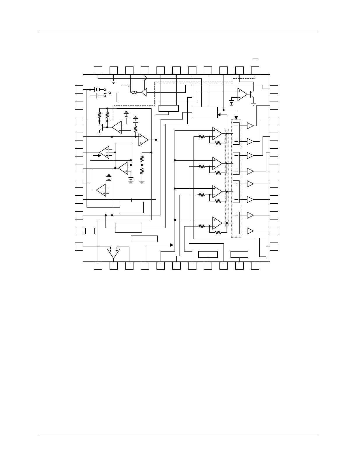
Internal Block Diagram
FIL SGND EMPSET ADPVCC
44
STOP
START CLKIN
PWM
DVCC
EMP
RST
34353637383940414243
OVP
BATT
RSTOUT
DEDSET
BDSW
ERRO
ERRI
SCP
COSC
NC
OPIN(-)
10
11
1
2
3
4
5
6
7
8
OVER
VOLTAGE
PROTECTION
9
TRIANGLE
NC
WAVE
SIGNAL VCC
STARTER
MAXIMUM
DETECTOIN
MUTE34
MUTE2
×
2
×
2
×
2
×
2
×
2
×
2
×
2
×
2
33
CHGSET
32
DO1(-)
31
DO1(+)
30
DO2(-)
29
DO2(+)
28
PGND
27
DO3(+)
DO3(-)
26
DO4(+)
25
24
DO4(-)
23
BRAKE
BRAKE
12 13 14 15 16 17 18 19 20 21 22
SVCC1 OPOUT OPIN(+) SVCC2
VREF
DI3 DI4
MUTE34
DI2
MUTE2
DI1
4
Page 5
FAN8038B(KA3038)
Absolute Maximum Ratings (Ta = 25°C)
Parameter Symbol Value Unit
Maximum Supply Voltage V
Maximum Output Current I
Power Dissipation P
Operating Temperature T
Stroage Temperature T
CC
O
D
OPR
STG
13.2 V
500 mA
1.0 W
-35 ~ +85 °C
-55 ~ +150 °C
Recommended Operating Conditions (Ta = 25°C)
Parameter Symbol Min. Typ. Max. Unit
Charging Circuit Power Supply Voltage ADPVCC 3.0 4.5 8.0 V
Power Supply Voltage BATT 1.5 2.4 8.0 V
Control Circuit Power Supply Voltage SVCC 2.7 3.2 5.5 V
PRE-Driver V
CC
Output Voltage VM - PWM BATT V
Operating Temperature Ta -10 25 70 °C
SVCC2 2.7 3.2 5.5 V
5
Page 6

FAN8038B(KA3038)
Electrical char ac teristics
(Ta=25°C, BATT=2.4V, SVCC1=SVCC2=3.2V, V
Parameter Symbol Conditions Min. Typ. Max. Unit
COMMON SECTION
BATT Stand-by Current I
BATT Supply Current (No Load) I
SVCC Supply Current (No Load) I
SVCC2 Supply Current (No Load) I
ADPVCC Supply Current
(No Load)
ST
BATT
SVCC1
SVCC2
I
ADPVCC
H-DRIVE PART
Voltage Gain CH1, 3, 4
CH2
Gain Error By Polarity ∆G
Input pin Resistance CH1, 3, 4
CH2
Maximum Output Voltage V
Saturation Voltage (Lower) V
Saturation Voltage (Upper) V
Input offset Voltage V
Output Offset Voltage CH1, 3, 4
CH2
DEAD Zone V
Brake1 On Voltage V
Brake1 Off Voltage V
MUTE2 On Voltage V
MUTE2 Off Voltage V
MUTE34 On Voltage V
MUTE34 Off Voltage V
VREF On Voltage V
VREF Off Voltage V
BRAKE1 Brake Current I
134
G
VC
G
VC
VC
R
DI1
R
DI2
OUT
SAT1
SAT2
IO
134
V
OO
V
OO
DB
M1ON
M1OFF
M2ON
M2OFF
M34ON
M34OFF
REFON
REFOFF
BRAKE
2
34
2
=1.6V, ADPVCC=0V, fCLKIN=88.2kHz)
REF
BATT=10.5V,SVCC1,
2=VREF=0V
--5µA
DVCC=0.45V, MUTE34=3.2V - 2.5 3.5 mA
DVCC=0.45V, MUTE34=3.2V,
ERRI=0V
-3.03.5mA
DVCC=0.45V, MUTE34=3.2V - 3.5 5.0 mA
ADPVCC=4.5V, ROUT=OPEN - 0.2 1.0 mA
-
12
21.51423.51624.5
--202dB
IN=1.7 & 1.8V
RL=8Ω, DVCC=BATT=4V,
IN=0 ~ 3.2V
11
6
7.5
1.9 2.1 - V
13
9
9
IO= -300mA, IN=0 & 3.2V - 240 400 mV
IO=300mA, IN=0 & 3.2V - 240 400 mV
--808mV
VREF=IN=1.6V
-70
-13000
70
130
--20020mV
DI1=1.8V 2.0 - - V
DI1=1.8V - - 0.8 V
DI2=1.8V 2.0 - - V
DI2=1.8V - - 0.8 V
DI3=DI4=1.8V - - 0.8 V
DI3=DI4=1.8V 2.0 - - V
INn=1.8V(N=1, 2, 3, 4) 1.2 - - V
INn=1.8V(N=1, 2, 3, 4) - - 0.8 V
Brake Current 4 7 10 mA
dB
KΩ
mV
*Granteed De sign Value
6
Page 7

FAN8038B(KA3038)
Electrical Characteristics
(Continued)
Parameter Symbol Conditions Min. Typ. Max. Unit
PWM POWER SUPPLY DRIVING
PWM Sink Current I
*DVCC Level Shift Voltage V
DVCC Leak Current I
*PWM Amp Transfer Gain G
PWM
SHIF
DLK
PWM
DI1=2.1V 10 13 17 mA
DI1=1.8V, DVCC-OUT1F 0.35 0.45 0.55 V
DVCC=9V, SVCC1,2=BATT=0V - 0 5 µA
DI1=1.8V, DVCC=1.2V ~ 1.4V 1/60 1/50 1/40 1/kΩ
DC/DC CONVERTER
ERROR AMP
SVCC1 Pin Threshold Voltage V
ERRO Pin Output Voltage H V
ERRO Pin Output Voltage L V
S1TH
EOH
EOL
ERRI=0.7V, IO = -100µA1.41.6-V
ERRI=1.3V, IO = 100µA--0.3V
- 3.05 3.20 3.35 V
SHORT CIRCUIT PROTECTION
SCP Pin Voltage V
SCP Pin Current 1 I
SCP Pin Current 2 I
SCP Pin Current 3 I
*SCP Pin Impedance R
SCP Pin Threshold Voltage V
Over Voltage Protection Detect V
SCP
SCP1
SCP2
SCP3
SCP
SCPTH
OVP
ERRI=1.3V - 0 0.1 V
ERRI=0.7V 6 10 16 µA
ERRI=1.3V, OFF=0V 12 20 32 µA
ERRI=1.3V, BATT=9.5V 12 20 32 µA
- 175 220 265 kΩ
ERRI=0.7V, COSC=470PF 1.10 1.20 1.30 V
OVP Voltage 9.5 10 10.5 V
TRANSISTOR DRIVING
BDSW Pin Output Voltage 1H V
SW1H
BATT=COSC=1.5V
=SVCC2=0V, 10mA
0.78 0.98 1.13 V
COSC=0V, IO = -10mA,
BDSW Pin Output Voltage 2H V
SW2H
ERRI=0.7V
1.0 1.5 - V
SCP=0V
BDSW Pin Output Voltage 2L V
BDSW Pin Oscillating Reequency1 f
SW Pin Oscillating Reequency 2 f
BDSW Pin Oscillating Reequency 3 f
*BDSW Pin Minimum Pulse Width T
Pulse Duty Start D
MAX. Pulse Duty at Self-Running D
MAX. Pulse Duty at CLKIN
Synchronization
SW2L
SW1
SW2
SW3
SWMIN
SW1
SW2
D
SW3
CT=2V, IO=1-mA - 0.3 0.45 V
COSC=470pF, =SVCC2=0V 65 80 95 kHz
COSC=470pF, CLKIN=0V 60 70 82 kHz
COSC=470pF - 88.2 - kHz
COSC=470pF,
ERRO=0.5 → 0.7V
COSC=470PF,
SVSS1,SVCC2=0V
COSC=470pF, ERR0=0.8V,
CLKIN=0V
0.01 - 0.6 µs
40 50 60 %
50 60 70 %
ERR0=0.8V, COSC=470pF 45 55 65 %
*Granteed De sign Value
7
Page 8

FAN8038B(KA3038)
Electrical Characteristics
(Continued)
Parameter Symbol Conditions Min. Typ. Max. Unit
DEAD TIME
*DEDSET Pin Impedance R
DEDSET Pin Output Voltage V
DEDSET
DEDSET
- 526578kΩ
- 0.78 0.88 0.98 V
INTERFACE
STOP Pin Threshold Voltage V
STOP Pin Bias Current I
START Pin On Threshold Voltage V
START Pin Off Threshold Voltage V
START Pin Bias Current I
CLKIN Pin Threshold Voltage H
CLKIN Pin Threshold Voltage L
V
V
CLKIN Pin Bias Current I
STOPTH
STOP
STATH1
STATH2
START
CLKINTH
H
CLKINTH
L
CLKIN
ERRI=1.3V 2.0 - - V
OFF=0V 75 95 115 µA
SVCC1,SVCC2=0V,
COSC=2V
SVCC1,SVCC2=0V,
COSC=2V
1.3 - - V
--2.1V
START=0V 13 16 19 µA
-2.0--V
---0.8V
CLKIN=3.2V - - 10 µA
START CURCUIT
Starter Switching Voltage V
Starter Switching Hysteresis Width V
Discharge Release Voltage V
SSV
SSHS
DIS
SVCC1,SVCC2=0V → 3.2V
START=0V
START=0V 130 200 300 mV
- 1.63 1.83 2.03 V
2.3 2.5 2.7 V
RESET CIRCUIT
*SVCC1 RESET Threshold Voltage
Ratio
RESET Detection Hysteresis Width V
RSTOUT Pin Output Voltage V
RSTOUT Pin Pull Up Resistance R
RST Pin Output Voltage 1 V
RST Pin Output Voltage 2 V
*RST Pin Pull Up Resistance R
R
RSTOTH
RSTHS
RSTO
RSTO
RST1
RST2
RST
- 859095%
- 25 50 100 mV
IO=1mA,
SVCC1,SVCC2=2.8V
- 72 90 108 kΩ
IO= -1mA,
SVCC1,SVCC2=2.8V
IO= -1mA,
SVCC1,SVCC2=0V
-7795113kΩ
--0.5V
2.0 - 2.4 V
2.0 - 2.4 V
*Granteed De sign Value
8
Page 9

FAN8038B(KA3038)
Electrical Characteristics
(Continued)
Parameter Symbol Conditions Min. Typ. Max. Unit
OP-AMP
Input Bias Current I
Input Offset Voltage V
High Level Output Voltage V
Low Level Output Voltage V
Output Drive Current (Source) V
SOURCE
Output Drive Current (Sink) V
BIAS
OFOP
OHOP
OLOP
SINK
IN(+)=1.6V - - 300 nA
IN(+)=1.6V -5.5 0 5.5 mV
RL=OPEN 2.8 - - V
RL=OPEN - - 0.2 V
50Ω GND - -6.5 -3.0 mA
50Ω SVCC 0.4 0.7 - mA
*Open Loop Voltage Gain GVO VIN= -75dB, F=1kHz - 70 - dB
*Slew Rate SR - - 0.5 - V/µs
BATTERY CHARGING CURCUIT
CHGSET Pin Bias Voltage V
*CHGSET Pin Output Resistance R
EMPSET Pin Leak Current 1 I
EMPSET Pin Leak Current 2 I
EMPSET Pin Saturation Voltage V
CHGSET
CHGSET
EMPSET
EMPSET
EMPSET
ADPVCC=4.5V,
CHGSET=1.8kΩ
ADPVCC=4.5V 0.75 0.95 1.20 kΩ
ADPVCC=4.5V,
CHGSET=OPEN
ADPVCC = 0.6V,
CHGSET = 1.8kΩ
ADPVCC = 4.5V, IO = 300mA,
CHGSET = 0Ω
0.71 0.81 0.91 V
--1.0µA
--1.0µA
- 0.45 1.0 V
EMPTY DETECTION
EMP Detection Voltge 1 V
EMP Detection Voltge 2 V
EMP Detection Hysteresis Voltage 1 V
EMP Detection Hysteresis Voltage 2 V
EMP Pin Output Voltage V
EMP Pin Output Leak Current I
*OVP Pin Input Resistance R
OVP Pin Leak Current I
EMP_SET Pin Detection Voltage V
EMP_SET Pin Detection Current I
EMPSET
EMPSET
EMPT1
EMPT2
EMHS1
EMHS2
EMP
EMPLK
OVP
OVPLK
V
EMPSET
I
EMPSET
V
EMPSET
I
EMPSET
= 0V 2.1 2.2 2.3 V
= -2µA 1.7 1.8 1.9 V
= 0V 25 50 100 mV
= -2µA 25 50 100 mV
IO = 1mA, OVP = 1V - - 0.5 V
OVP = 2.4V - - 1.0 µA
V
EMPSET
SVCC1 = SVCC2 = 0V,
OVP = 4.5V
V
EMPSET
OVP = 2V
= 0V 17 23 27 kΩ
--1.0V
= BATT-
EMPSET
,
1.5 - - V
EMPSET -2 - - µA
*Granteed De sign Value
9
Page 10

FAN8038B(KA3038)
Application Information
1. Mute Function
• When The BRAKE Pin is low is normal opration (high is CH1 mute on).
• When The Mute2 Pin is low is normal opration (high is CH2 mute on).
• When The Mute34 Pin is high is normal opration (low is CH3,4 mute on).
2. Vref Drop Mute (Figure 1)
• When the Voltage of the mute pin is above 1V, the mute circuit is stopped and the output circuit is.
VCC
CH Bias Block
VREF
Figure 1. VREF Drop MUTE Circuit Figure 2. TSD Circuit
Hysteresis
VCC
Q1
2
CH Bias Block
1
ircuit
ircuitircuit
3. Thermal Shutdown(Figure 2)
• If the chip temperature rises above 150°C, then the thermal shutdown (TSD) circuit is activated and the output circuit will
be mute.
4. H-bridge Driver (4-Channels)
Driver input resistance is 10kΩ of CH1, CH3, CH4 and input resistance of CH2 is 7.5kΩ.
Driver gain can obtain under -mentioned
CH1, 3, 4: GV 20
CH2 GV = 20log
R is External resistance.
10
log=
---------------------
11K R+
110K
---------------------- -
7.5K R+
55K
Page 11

5. Switching Regulated Power Supply Drive
• This circuit detects a maximum output value of 4CH drivers and then generates PWM Signal.
• External Component is PNP-Tr, Coil, Schottky Diodeand Capacitor .
BUCK
CON.
HVCC
AMP
FAN8038B(KA3038)
HVCC
OSC
OUTPUT
LEVEL DET.
Figure 1. Switching Regulated Power Supply
6. DC/DC Converter Control Circuit
• Booster circuit needs External component. and the voltage() is defined as follows.
R1 Resistor1=
R2 Resistor2=
R3 30KΩ=
R4 30.5KΩ=
30k
30.5k
SVCC1 1.267
R1 R3⋅
--------------------- R1 R3+
---------------------------------------------------
×=
R2 R4⋅
--------------------- R2 R4+
12
R1
7
R2 R4⋅
--------------------- -+
R2 R4+
R2
Figure 2. Output Voltage
11
Page 12

FAN8038B(KA3038)
• Short Circuit Protection function when GND and is short, ERRI become LOW and ERRO HIGH and it makes capacitor
charging. fanally AMP3 is OFF.(figure 5)
BATT
SVCC
1
AMP4
30K
30.5K
AMP1
AMP5
AMP3
SCP
1.267V
1.267V
DEDSET
COSC
Figure 3. DC/DC Converter Control Circuit
Switching off time depen on a capacitor of the SCP . and the equation is as follow.
V
TH
----------- -
tC
×= V
SCP
I
SCP
TH
1.25V, I
SPRT
10µA==()
• Max Duty can be controlled resistor. the equation is as follow.
tC
DEDSET
R×= R65KΩ=()
• Capacitor of the SCP terminal can control disable switiching time and it can be calculated by as follow equation.
V
TH
---------------
tC
• Over Voltage Protection BATT Voltage is over 9.7V charging SCP terminal Capacitor, it reach to V
×= V
SCP
I
STOP
TH
1.25V, I
20µA==()
OFF
SW terminal signal
TH
is OFF the equation is as follow
V
TH
tC
----------
×= V
SCP
I
HV
TH
1.25V, I
20µA==()
HV
• If Output Voltage of RSTOUT Circuit DC/DC Conver is over than 90%, RSTOUT terminal turn to HIGH and Hysteresis is
50mV. and RSTOUT stste is ON.
7. Empty Detecting Circuit.
EMPSET Detect Voltage Hysteresis Mode
LOW 2.2V 50mV Battery Mode
HIGH-Z 1.8V 50mV Adapter Mode
8. Battery Charging Circuit
• the battery charger circuit is s e parated from an y other block .
• TSD operate at 150°C. Hysteresis is 30°C
12
Page 13

Typical Performance Cha ra cte ristic s
FAN8038B(KA3038)
S1TH
V
[V ]
ST
I
[mA]
Temp vs V
S1TH
3.20
3.18
3.15
3.13
3.10
3.08
3.05
-35 -20 -5 10 25 40 55 70 85
Temp [℃]
0.1
BATT vs I
0.05
0
-0.05
-0.1
1.5 2.5 3.5 4.5 5.5 6.5 7.5
ST
BATT[V ]
Temp vs Vovp
10.50
10.25
Vovp
10.00
[V ]
9.75
9.50
-35 -20 -5 10 25 40 55 70 85
Temp [℃]
BAT T vs IBATT
4
3
IBATT
2
[mA]
1
0
1.5 2.5 3.5 4.5 5.5 6.5 7.5
BAT T [V ]
EMPSET
V
[V ]
Temp vs VEMPSET
1.8
1.6
1.4
1.2
1
-35 -20 -5 10 25 40 55 70 85
Temp [℃]
ISINK
[mA]
Temp vs ISINK
1
0.9
0.8
0.7
0.6
0.5
0.4
-35 -20 -5 10 25 40 55 70 85
Temp [℃]
13
Page 14

FAN8038B(KA3038)
Application Circuits
ADT VCC
220uF
220uF
TO MICOM
DC/DC
CONVERTER
104
8.2k
223
1uF
`
470p
Filter
OFF
100k 102
ON
33uF
47Ω
44
1
2
STARTER
MAXIMUM
DETECTOIN
3
4
5
6
7
8
OVER
VOLTAGE
PROTECT ION
9
TRIANGLE
10
NC
WAVE
SIGNAL VCC
11
MUTE34
12 13 14 15 16 17 18 19 20 21 22
TO MICOM
0.1uF
220uF
34353637383940414243
CHG SETTING RES
33
32
M
31
30
29
28
27
26
25
24
23
SLED
MOTOR
M
SPINDLE
MOTOR
TRK
ACTUATOR
FOC
ACTUATOR
FROM MICOM
0.1uF
MUTE2
2
×
× 2
×
2
×
2
×
2
×
2
×
2
×
2
BRAKE1
14
FROM MICOM
SERVO
FROM MICOM
Page 15

FAN8038B(KA3038)
15
Page 16

FAN8038B(KA3038)
DISCLAIMER
FAIRCHILD SEMICONDUCTOR RESERVES THE RIGHT TO MAKE CHANGES WITHOUT FURT HER NOTICE TO ANY
PRODUCTS HEREI N TO IMPROVE RELIABILITY, FUNCTIO N OR DESIGN. FAIRCH IL D DOES NOT ASSUME ANY
LIABILITY ARISING OUT OF THE APPLICATION OR USE OF ANY PRODUCT OR CIRCUIT DESCRIBED HEREIN; NEITHER
DOES IT CONVEY ANY LICENSE UNDER IT S PATENT RIGHTS, NOR THE RIGHTS OF OTHE RS.
LIFE SUPPORT POL I CY
FAIRCHILD’S PR ODUCTS ARE NOT AUTH ORIZED FOR USE AS C RITICAL COMPONENT S IN LIFE SUPPORT DE VICES
OR SYSTEMS WITHOUT THE EXPRESS WRITTEN APPROVAL OF THE PRESIDENT OF FAIRCHILD SEMICONDUCTOR
CORPORATION. As used herein :
1. Life support devices or systems are devices or systems
which, (a) are intended for surgical implant into the body,
or (b) support or sustain life, and (c) whose failure to
perform when properly used in accordance with
2. A critical component in any component of a life support
device or sy stem whose fai lure to perform can be
reasonably expec ted to cause the failur e of the life support
device or system, or to affect its safety or effec t iv ene ss .
instructions for use provided in the labeling, can be
reasonably expected to result in a significant injury of the
user.
www.fairchildsemi.com
9/6/02 0.0m 001
2002 Fairchild Semiconductor Corporation
Stock#DSxxxxxxxx
 Loading...