

Datasheet EM564081BC-85E, EM564081BC-85, EM564081BC-70E, EM564081BC-70, EM564081BA-85E Datasheet (ETRON)
...Page 1
EtronTech
EM564081
512K x 8 Low Power SRAM
Preliminary, Rev 0.7 01/2001
Features
• Single power supply voltage of 2.3V to 3.6V
• Power down features using CE1# and CE2
• Low power dissipation
• Data retention supply voltage: 1.0V to 3.6V
• Direct TTL compatibility for all input and output
• Wide operating temperature range: -40°C to 85°C
• Standby current @ VDD = 3.6 V
I
DDS2
Typical Maximum
EM564081BA/BC-70/85
EM564081BA/BC-70E/85E
1 µA 10 µA
5 µA 80 µA
Ordering Information
Part Number Speed I
EM564081BC-70 70 ns
EM564081BC-70E 70 ns
EM564081BA-70 70 ns
EM564081BA-70E 70 ns
EM564081BC-85 85 ns
EM564081BC-85E 85 ns
EM564081BA-85 85 ns
EM564081BA-85E 85 ns
DDS2
10 µA
80 µA
10 µA
80 µA
10 µA
80 µA
10 µA
80 µA
Package
6x8 BGA
6x8 BGA
8x10 BGA
8x10 BGA
6x8 BGA
6x8 BGA
8x10 BGA
8x10 BGA
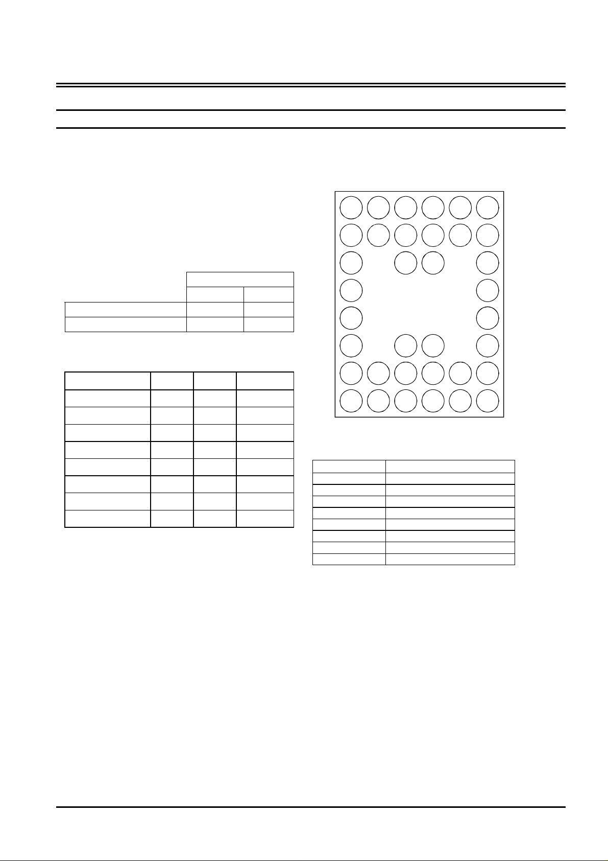
Pin Configuration
36-Ball BGA (CSP), Top View
1 2 3 4 5 6
A
A0 A1
B
DQ4 A2
C
DQ5 NC A5 DQ1
D
GND VDD
E
VDD GND
F
DQ6 A18
G
DQ7
H
A9 A10
OE#
WE#
CE1#
A3 A6 A8
CE2
A4 A7 DQ0
A17
A16 A15 DQ3
A12 A13 A14
A11
Pin Description
Symbol Function
A0 - A18 Address Inputs
DQ0 – DQ7 Data Inputs / Outputs
CE1#, CE2 Chip Enable Inputs
OE# Output Enable
WE# Read / Write Control Input
GND Ground
V
DD
NC No Connection
Power Supply
DQ2
Overview
The EM564081 is a 4,194,304-bit SRAM organized as 512K by 8 bits. It is designed with advanced CMOS
technology. This Device operates from a single 2.3V to 3.6V power supply. Advanced circuit technology
provides both high speed and low power. It is automatically placed in low-power mode when chip enable (CE1#)
is asserted high or (CE2) is asserted low. There are three control inputs. CE1# and CE2 are used to select the
device and for data retention control, and output enable (OE#) provides fast memory access. This device is
well suited to various microprocessor system applications where high speed, low power and battery backup are
required. And, with a guaranteed operating range from -40°C to 85°C, the EM564081 can be used in
environments exhibiting extreme temperature conditions.
Etron Technology, Inc.
No. 6, Technology Rd. V, Science-Based Industrial Park, Hsinchu, Taiwan 30077, R.O.C.
TEL: (886)-3-5782345 FAX: (886)-3-5778671
Etron Technology, Inc., reserves the right to make changes to its products and specifications without notice.
Page 2
EtronTech
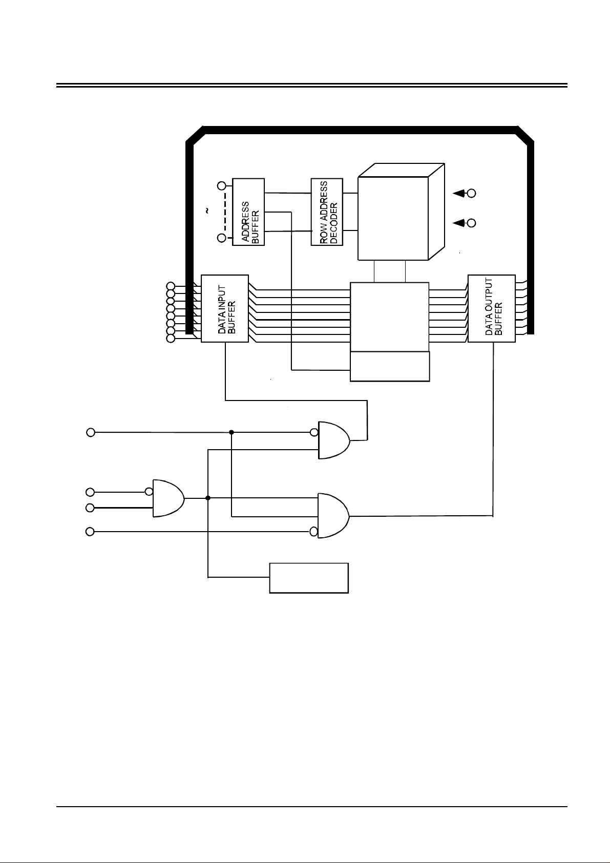
Block Diagram
EM564081
WE#
DQ0
DQ1
DQ2
DQ3
DQ4
DQ5
DQ6
DQ7
A0
A18
MEMO RY
CELL ARRAY
512KX8
SENSE AMP
COLUMN ADDRESS
DECODER
VDD
GND
CE1#
CE2
OE#
POWER DOWN
CIRCUIT
Preliminary
2 Rev 0.7
January 2001
Page 3
EtronTech
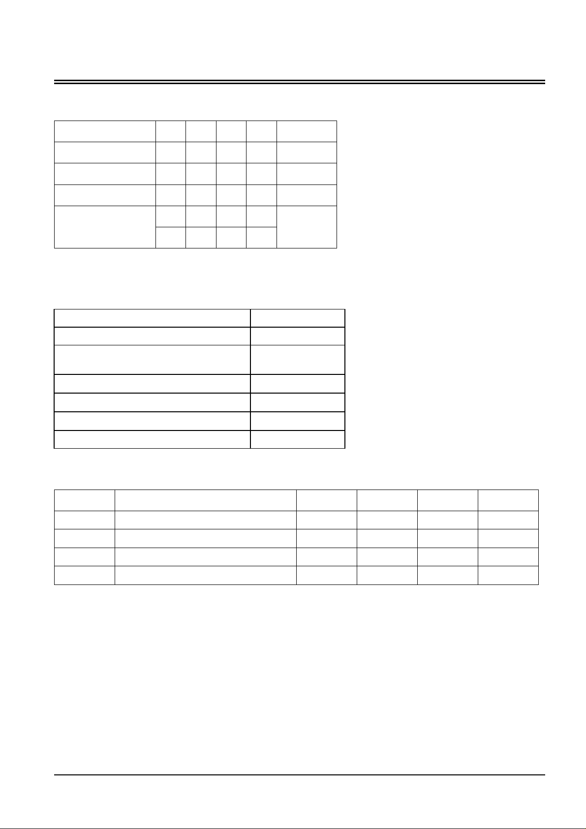
Operating Mode
Mode CE1# CE2 OE# WE# DQ0~DQ7
EM564081
Read L H L H D
Write L H X L D
Output Deselect L H H H High-Z
H X X X
Standby
X L X X
High-Z
Note: X = don't care. H=logic high. L=logic low.
Absolute Maximum Ratings
Supply voltage, V
Input voltages, V
Input and output voltages, V
Operating temperature, T
Storage temperature, T
Soldering Temperature (10s), T
Power dissipation, P
DD
IN
I/O
OPR
STRG
D
SOLDER
-0.3 to +4.6V
-0.3 to +4.6V
-0.5 to V
-40 to +85°C
-55 to +150°C
OUT
IN
DD
+0.5V
260°C
0.6 W
DC Recommended Operating Conditions (Ta=-40°C to 85°C)
Symbol Parameter Min Typ Max Unit
V
DD
V
IH
V
IL
V
DR
Note:
(1) Overshoot : VDD +2.0V in case of pulse width ≤ 20ns
(2) Undershoot : -2.0V in case of pulse width ≤ 20ns
Power Supply Voltage 2.3
Input High Voltage 2.2
Input Low Voltage -0.3
Data Retention Supply Voltage 1.0
(2)
−
−
−
−
3.6 V
V
+ 0.3
DD
0.6 V
3.6 V
(1)
V
Preliminary
3 Rev 0.7
January 2001
Page 4
EtronTech
EM564081
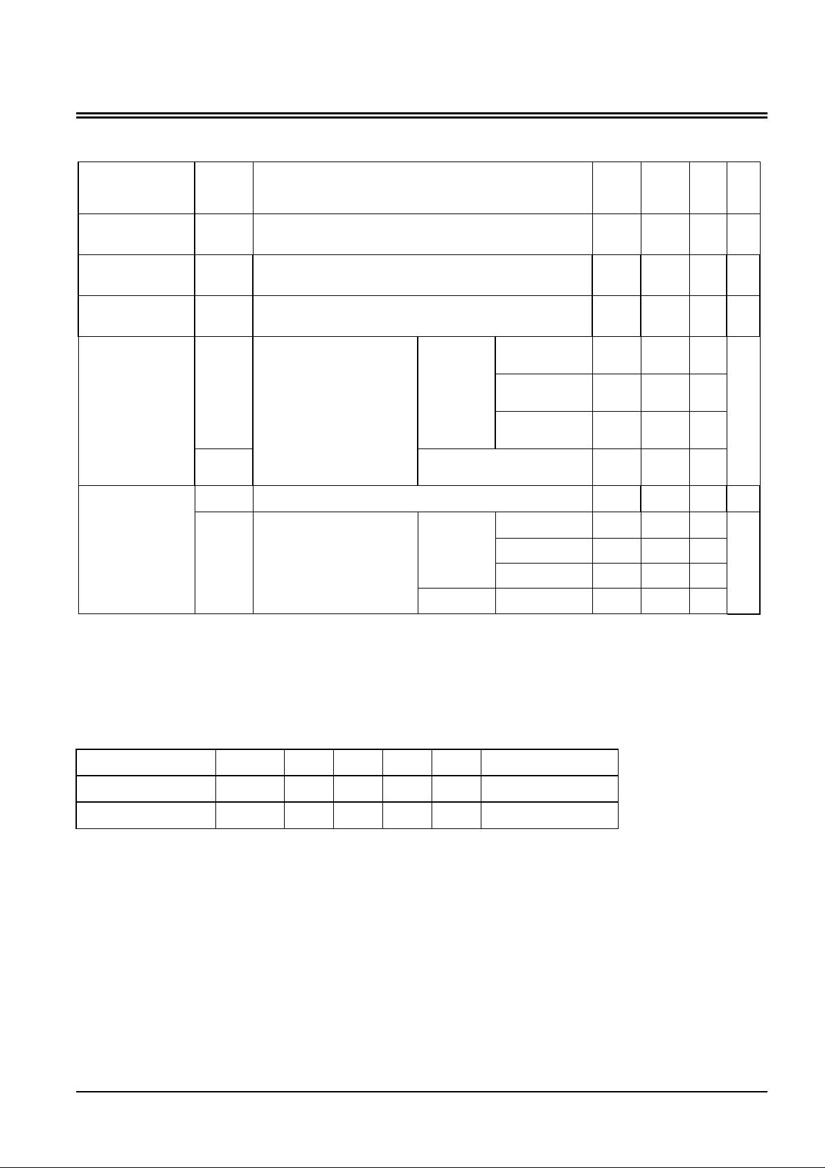
DC Characteristics (Ta = -40°C to 85°C, VDD = 2.3V to 3.6V)
Parameter Symbol Test Conditions Min Typ* Max Unit
Input low current I
Output low
voltage
Output high
voltage
Operating current
Standby current
Notes:
* Typical value are measured at Ta = 25°C.
** In standby mode with CE1# ≥ VDD - 0.2V, these limits are assured for the condition
CE2 ≥ V
- 0.2V or CE2 ≤ 0.2V.
DD
V
V
OH
DD1
I
DD2
I
DDS1
I
DDS2
(Note)
IL
OL
I
= 0V to V
IN
I
= 2.1 mA -
OL
I
= -1.0 mA
OH
CE1# = V
CE2 = V
I
OUT
Other Input = V
CE1# = V
CE1# = V
**
CE2 = 0.2V
IL
IH
= 0mA
IH
DD
DD
and
and
/ V
IH
or CE2 = V
– 0.2V or
Cycle time
IL
IL
-70/85
-70E/85E V
V
DD
V
V
V
V
V
DD
DD
DD
DD
DD
DD
= min
Cycle time = 1µs
= 3.6 V
= 2.7 V
= 2.3 V
= 3.6 V
= 2.7 V
= 2.3 V
= 3.6 V
- 1
VDD -
0.15
−
−
−
− −
− −
−
−
−
−
−
0.4 V
−
− −
15 25
10 15I
7 12
0.5 mA
1 10
0.8 5
0.5 3
5 80
1
µA
V
mA
5
µA
Capacitance (Ta = 25°C; f = 1 MHz)
Parameter Symbol Min Typ Max Unit Test Conditions
Input capacitance C
Output capacitance C
Notes:
This parameter is periodically sampled and is not 100% tested.
Preliminary
IN
OUT
− −
− −
10 pF VIN = GND
10 pF V
OUT
= GND
4 Rev 0.7
January 2001
Page 5

EtronTech
EM564081
AC Characteristics and Operating Conditions (Ta = -40°C to 85°C, VDD = 2.3V to 3.6V)
Read Cycle
EM564081
Symbol Parameter
-85 -70
Min Max Min Max
Unit
t
RC
t
AA
t
CO1
t
CO2
t
OE
t
LZ
t
OLZ
t
HZ
t
OHZ
t
OH
Write Cycle
Symbol Parameter
t
WC
t
WP
t
CW
t
AS
t
WR
t
WHZ
t
OW
t
DS
t
DH
Read cycle time 85
Address access time
Chip Enable (CE1#) Access Time
Chip Enable (CE2) Access Time
Output enable access time
Chip Enable Low to Output in Low-Z 10
Output enable Low to Output in Low-Z 3
Chip Enable High to Output in High-Z
Output Enable High to Output in High-Z
Output Data Hold Time 10
Write cycle time 85
Write pulse width 55
Chip Enable to end of write 70
Address setup time 0
Write Recovery time 0
WE# Low to Output in High-Z
WE# High to Output in Low-Z 5
Data Setup Time 35
Data Hold Time 0
70
−
85
−
85
−
85
−
45
−
−
−
35
−
35
−
−
EM564081
-85 -70
Min Max Min Max
−
−
−
−
−
35
−
−
−
−
−
−
−
−
10
3
−
−
10
70
55
60
0
0
−
5
30
0
−
70
70
70
35
−
−
25
25
−
−
−
−
−
−
30
−
−
−
ns
Unit
ns
AC Test Condition
• Output load: 50pF + one TTL gate
• Input pulse level: 0.4V, 2.4V
• Timing measurements: 0.5 x V
• tR, tF: 5ns
DD
Preliminary
5 Rev 0.7
January 2001
Page 6

EtronTech
Read Cycle
(See Note 1)
Address
t
EM564081
RC
CE1#
CE2
O E#
t
HZ
t
OH
t
AA
t
CO1
t
CO2
t
OE
D
OUT
Preliminary
t
OHZ
t
OLZ
t
LZ
VALID DAT A OUT
6 Rev 0.7
January 2001
Page 7

EtronTech
Write Cycle1
(WE# Controlled)(See Note 4)
Address
t
W C
EM564081
WE#
CE1#
CE2
D
OUT
t
AS
t
WHZ
(See Note2) (See Note3)
t
t
CW
CW
t
WP
t
W R
t
OW
D
IN
Preliminary
(See Note 5)
t
DS
VALID DATA IN (See Note 5)
7 Rev 0.7
t
DH
January 2001
Page 8

EtronTech
Write Cycle 2
(CE1# Controlled)(See Note 4)
Address
t
WC
EM564081
WE#
CE1#
CE2
D
OUT
t
AS
t
W HZ
t
LZ
t
t
CW
CW
t
WP
t
DS
t
t
WR
DH
D
IN
Preliminary
(See Not e 5) VALID DATA IN
8 Rev 0.7
January 2001
Page 9

EtronTech
Write Cycle 3
(CE2 Controlled)(See Note 4)
Address
t
EM564081
W C
WE#
CE1#
CE2
D
OUT
t
AS
t
W P
t
CW
t
CW
t
WHZ
t
LZ
t
DS
t
t
W R
DH
D
IN
(See Note 5) VALID DATA IN
Note:
1. WE# remains HIGH for the read cycle.
2. If CE1# goes LOW (or CE2 goes HIGH) with or after WE# goes LOW, the outputs will remain at high
impedance.
3. If CE1# goes HIGH (or CE2 goes LOW) coincident with or before WE# goes HIGH, the outputs will remain
at high impedance.
4. If OE# is HIGH during the write cycle, the outputs will remain at high impedance.
5. Because I/O signals may be in the output state at this time, input signals of reverse polarity must not be
applied.
Preliminary
9 Rev 0.7
January 2001
Page 10

EtronTech
EM564081
Data Retention Characteristics (Ta = -40°C to 85°C)
Symbol Parameter Min Typ Max Unit
V
Data Retention Supply
DR
Voltage
CE1# ≥ V
VIN ≥ V
- 0.2V, CE2 ≤ 0.2V,
DD
- 0.2V or VIN ≤ 0.2V
DD
VDD = 1.0V, CE1# ≥ V
I
Data Retention Current
DR
CE2 ≤ 0.2V, VIN ≥ V
VIN ≤ 0.2V
t
SDR
t
RDR
Chip Deselect to Data Retention Mode Time 0
Recovery Time t
CE1# Controlled Data Retention Mode (see Note1)
V
V
DD
2.7V
V
IH
CE1
DD
t
SD R
DATA RETENTION MOD E
VDD - 0.2V
DD
- 0.2V or
DD
- 0.2V,
1.0
−
RC
t
RDR
3.6 V
−
0.5 3.5
− −
− −
µA
ns
ns
GN D
CE2 Controlled Data Retention Mode (see Note2)
V
DD
2.7V
V
IH
V
IL
GND
CE2
V
DD
t
SDR
DATA RE TENTION MODE
0.2V
t
RDR
Note:
1. If CE1# controlled data retention mode, minimum standby current mode is entered when CE2 ≤ 0.2V or
CE2 ≥ VDD - 0.2V.
2. In CE2 controlled data retention mode, minimum standby current mode is entered when CE2 ≤ 0.2V.
Preliminary
10 Rev 0.7
January 2001
Page 11

EtronTech
Package Diagrams
36-Ball (6mm x 8mm) BGA
Units in mm
EM564081
TOP VIEW
PIN 1 CORNER
1 2 3 4 5 6
- B -
BOTTOM VIEW
0.10SS C
0.25
0.30 0.05(48X)
6 5 4 3 2 1
PIN 1 CORNER
C A B
- C - SEATIN G PLANE
- A -
0.20(4X)
0.15
0.75
3.75
Preliminary
11 Rev 0.7
January 2001
Page 12

EtronTech
Package Diagrams
36-Ball (8mm x 10mm) BGA
Units in mm
EM564081
TOP VIEW
PIN 1 CORNER
1 2 3 4 5 6
BOTTOM VIEW
0.10SS C
0.25
0.30 0.05(48X)
6 5 4 3 2 1
PIN 1 CORNER
C A B
- C - SEATIN G PLANE
- B -
0.20( 4X)
- A -
0.15
0.75
3.75
Preliminary
12 Rev 0.7
January 2001
 Loading...