

Page 1
1M Home Phoneli ne Network P hysi cal Layer Si ngle Chi p Transcei ver
General Descri ption
The DM9801 is a physical-layer, single-chip, low-power
transceiver for 1M Home Phoneline Network applications.
On the media side, it provides an interface to a Ho me
Phoneline wiring system. The reconciliation layer interfaces
to the DM9801 either through an IEEE802.3u subset Media
Independent Interface (MII) or a pseudo-standard General
Purpose Serial Interface (GPSI). A management interface is
provided by MDIO/MDC when operating in MII mode, or a
Serial Peripheral Interface bus when operating in GPSI
mode.
Block Diagram
DM9801
The DM9801 uses a low-power and high-performance
CMOS process. It contains the entire physical layer
functions of 1M as defined by Home Phoneline Network
Alliance, Rev. 1.1, including the Physical Coding
Sublayer, (RLL25) Encoder/Decoder (ENC/DEC), 4-wire
HN Driver circuit and receiver an alog front end (AFE).
Patent-Pending Circuitry Includes:
An enhanced 4-wire Home Network transceiver circuit.
GPSI - MII
Transmit
GPSI - MII
Receive
Interface
Select
Muxed
GPSI
or Mii
Interface
RLL25
Encoder
Master
PHY
Controller
RLL25
Decoder
Transmit
Timing
Generator
Receiever
and
Digital PLL
HN
Secondary
Driver
HN
Primary
Driver
Receiver
AFE
HNB+/-
HNA+/-
Preliminary 1
Version: DM9801-DS-P 02
March 20, 2000
Page 2

1M Home Phoneli ne Network P hysi cal Layer Si ngle Chi p Transcei ver
Features
DM9801
• 1M Home Phoneline Network physical-layer, single-
chip transceiver
• Supports the MII including the MDIO/MDC serial
management interface
• Supports the GPSI including a SPI serial
management interface
• Supports Link Integrity function
• Smart equalizer circuit for 1M receiver
• Supports Patent Pending 4-wire operation
• Supports hardware or software speed select
• Supports Interrupt on change, eliminates
management polling
• Flexible buil t-in LE D support for TX Activity, RX
Activity and Collision Indication or Activity, Link state
and Collision
• Digital PLL circuit using advanced digital algorithm to
reduce jitter
• Low-power, high-performance CMOS process
• Available in a s mall outline 100- pin LQFP
• 3.3V DC p ow e r w ith 5V DC tol erant I/O
2 Preliminary
Version: DM9801-DS-P 02
March 20, 2000
Page 3

1M Home Phoneline Netwo rk Physical La yer Si ngle Chip T ranscei ver
Pin Configu ration: DM9801, 100-pin LQFP
RXD1
NC
NC
NC
RXD0(SRXDAT)
RXD3
RXD2
CRS
COL(CLSN)
NC
RX_DV(SO)
RX_CLK(SRDCLK)
TX_CLK(STDCLK)
NC
DGND
TXD0(STXDAT
TXD1(BP1)
TXD3(SMODE)
TX_EN(STXEN)
TXD2(SI)
NC
NC
DGND
DM9801
NC
NC
NC
NC
NC
DVCC
NC
INT#
LNKSTA
PHYAD1
PHYAD2
PHYAD3
COLLED#
RXLED#(LNKLED#)
TXLED#(ACTLED#)
DGND
NC
NC
NC
NC
AVCC
NC
BGREF
BGGND
NC
NC
NC
1
2
3
4
5
6
7
8
9
10
11
12
13
14
15
16
17
18
19
20
21
22
23
24
25
9998979695
100
26
27
29
28
949392
30
3132333435
91
908988
87
DM9801E
3738394041
36
8685848382
44
42
43
8079787776
81
454647
48
49
50
75
74
73
72
71
70
69
68
67
66
65
64
63
62
61
60
59
58
57
56
55
54
53
52
51
NC
NC
NC
DVCC
DVCC
NC
NC
PHYAD0
MDIO(SCS#)
MDC(BP0)
TRIDRV
RESET#
CONFIG0
CONFIG1
INTFSEL
CMDENA
SPDSEL
PWSEL
FWENA
NC
DGND
NC
TSTMODE
NC
NC
NC
NC
AGND
NC
AGND
NC
NC
AVCC
AVCC
NC
HNPA
HNNA
AGND
AGND
HNPB
HNNB
NC
NC
AVCC
XTAL1
XTAL2
NC
DGND
PHYAD4
NC
Preliminary 3
Version: DM9801-DS-P 02
March 20, 2000
Page 4

1M Home Phoneli ne Network P hysi cal Layer Si ngle Chi p Transcei ver
Pin Descr iption
Pin No. Pin Name I/O Description
Station Interface: Receive Data, Transmit Data and Management
85 TXD0
or
STXDAT
84 TXD1
or
BP1
83 TXD2
or
SI
82 TXD3
or
SMODE
86 TX_CLK
or
STDCLK
81 TX_EN
or
STXEN
66 MDC
or
BP0
O,Z
Transmit Data Bit 0 (MII Mode, INTFSEL = 0):
I
Transmit data input pin, bit 0, for nibble data from the MI I
Serial Transmit Data Bit (GPSI Mode, INTFSEL = 1):
Transmit data input pin for serial data from the GPSI.
Transmit Data Bit 1 (MII Mode, INTFSEL = 0):
I
Transmit data input pin, bit 1, for nibble data from the MI I
SPROM Boot Page Select 1 (GPSI Mode, INTFSEL = 1):
Most significant bit of a 2-bit encoded select. The BP1 and BP0 inputs, select
one of four, 64-byte, SPROM pages to initialize the DM9801 management
registers. Master mode must be selected using the SMODE input.
Transmit Data Bit 2 (MII Mode, INTFSEL = 0):
I
Transmit data input pin, bit 2, for nibble data from the MI I
Serial Data Input (GPSI Mode, INTFSEL = 1):
This is the serial data input pin to the DM9801 for the SPI bus. The SPI bus
operation is only valid if GPSI mode is select ed.
Transmit Data Bit 3 (MII Mode, INTFSEL = 0):
I
Transmit data input pin, bit 3, for nibble data from the MI I
Serial Mode Select (GPSI Mode, INTFSEL = 1):
This input pin selects the SPI buses mode of oper ation. The SPI bus modes
of operation are:
Master Mode (SMODE = 0)
Slave Mode (SMODE = 1)
The SPI bus operation is only v alid if GPSI mode is selected.
MII Transmit Clock (MII Mode, INTFSEL = 0):
TX_CLK is an output pin from the DM9801. Used as the transmit data
reference clock, to clock in nibble data from the M I I when in MII interface
mode.
Serial Transmit Data Clock (GPSI Mode, INTFSEL = 1):
STDCLK is an output from the DM9801. Used as the transmit reference clock
to clock in the STXDATA when in GPSI interface mode.
MII Transmit Enable (MII Mode, INTFSEL = 0):
I
MII Transmit enable input, used to enable the transmit function of the MII
when in MII interface mode.
Serial Transmit Enable (GPSI Mode, INTFSEL = 1):
Used to enable the transmit function of the GPSI when in GPSI interface
mode.
MII Serial Management Clock (MII Mode, INTFSEL = 0):
I
Synchronous clock to the MDIO management data input/output serial
interfac e which is asynchronous to transmit and receive clocks. The
maximum clock rate is 2.5MHz.
SPROM Boot Page Select 0 (GPSI Mode, INTFSEL = 1):
Least significant bit of a 2-bit encoded select. The BP1 and BP0 inputs,
select one of four, 64-byte, SPROM pages to initialize the DM 9801
management registers. Master mode must be selected using the SMODE
input.
DM9801
4 Preliminary
Version: DM9801-DS-P 02
March 20, 2000
Page 5

DM9801
1M Home Phoneline Netwo rk Physical La yer Si ngle Chip T ranscei ver
Pin Descr iption
(Continued)
Pin No. Pin Name I/O Description
Station Interface: Receive Data, Transmit Data and Management (Continued)
67 MDIO
Or
SCS#
97 RXD0
Or
SRXDAT
96 RXD1 O,Z
95 RXD2 O,Z
94 RXD3 O,Z
90 RX_CLK
Or
SRDCLK
91 RX_DV
Or
SO
93 CRS O,Z
92 COL
or
CLSN
I/O,Z
O,Z
O,Z
O,Z
O,Z
MII Serial Management Data (MII Mode, INTFSEL = 0):
Bi-directional management instruction/data signal that may be driven by the
station management entity or the PHY. This pin requir es a 1.5KΩ pull-up
resistor.
Serial Interf ace Chip Select (GPSI M od e, INTFSEL = 1):
SCS# is a bi-directional management chip select signal that may be driven
by the station management entity or the PHY. (Active low)
Receive Data Bit 0 (MII Mode, INTFSEL = 0):
Receive data output pin, bit 0, for nibble data to the MII
Serial Receive Data Bit (GPSI Mode, INTFSEL = 1):
Receive data output pin for serial data to the GPSI.
Receive Data Bit 1:
Receive data output pin, bit 1, for nibble data to the
Receive Data Bit 2:
Receive data output pin, bit 2, for nibble data to the MII
Receive Data Bit 3:
Receive data output pin, bit 3, for nibble data to the MII
MII Receive Clock (MII Mode, INTFSEL = 0):
RX_CLK is an output pin from the DM9801. Used as the receive data
reference clock, to clock out nibble data from the MII when in MII interface
mode.
Serial Receive Data Clock (GPSI Mode, INTFSEL = 1):
SRDCLK is an output from th e DM9801. Used as the receive reference
clock to clock out the SRXDATA when in GPSI interface mode.
Receive Data Valid (MII Mode, INTFSEL = 0):
RX_DV is asserted high to indicate that valid data is present on RXD[3:0].
Serial Data Output (GPSI Mode, INTFSEL = 1):
This is the serial data output pin from the DM9801 fo r the SPI bus. The SPI
bus operation is only v alid if GPS I mode i s selected.
Carrier Sense:
This pin is asserted high to indicate the presence of carrier due to receive
or transmit activities.
Collision Detect MII Mode, INTFSEL = 0):
COL is asserted high to indicat e dete ction of collision condition.
Collisi on De tect (GPS I M o de , INTFS E L = 1 ) :
CLSN is asserted high to indicate detection of collision condition.
Preliminary 5
Version: DM9801-DS-P 02
March 20, 2000
Page 6

DM9801
1M Home Phoneli ne Network P hysi cal Layer Si ngle Chi p Transcei ver
Pin Descr iption
PHY Address Interface:
PHYAD[4:0] provides up to 32 unique PHY address. An address selection of all zeros (00000) will result in a
PHY isolation condition. See the isolate bit description in the BMCR, address 00.
68 PHYADSEL
8 PHYAD1 I/O,
9 PHYAD2 I/O,
10 PHYAD3 I/O,
47 PHYAD4 I/O,
(Continued)
(PHYAD0)
Or
SCLK
I/O,Z
Z
Z
Z
Z
MII Serial Management PHY Address Select (MII Mode, INTFSEL = 0):
PHYADSEL is an input signal that selec ts one of two PHY addresses within
the 32 address range for the DM9801 MII management inter fa ce when both
CONFIG1 and CONFIG0 are not set to 1.
0 = 0x01 address
1 = 0x1F address
PHY Address 0 (MII Mode, INTFSEL = 0):
PHY address bit 0 for mult iple PH Y address applications. Both CONFIG1
and CONFIG0 must be set to 1.
Serial Interface Clock (GPSI Mode, INTFSEL = 1):
SCLK is a bi-directional clock signal used to synchronize SI, SO and SCS#
to and from the DM9801 SPI bus.
PHY Address 1 (MII Mode, INTFSEL = 0):
PHY address bit 1 for mult iple PH Y address applications. Both CONFIG1
and CONFIG0 must be set to 1. Leave unconnected when both CONFIG1
and CONFIG0 are not 1.
PHY Address 2 (MII Mode, INTFSEL = 0):
PHY address bit 2 for mult iple PH Y address applications. Both CONFIG1
and CONFIG0 must be set to 1. Leave unconnected when both CONFIG1
and CONFIG0 are not 1.
PHY Address 3 (MII Mode, INTFSEL = 0):
PHY address bit 3 for mult iple PH Y address applications. Both CONFIG1
and CONFIG0 must be set to 1. Leave unconnected when both CONFIG1
and CONFIG0 are not 1.
PHY Address 4 (MII Mode, INTFSEL = 0):
PHY address bit 4 for mult iple PH Y address applications. Both CONFIG1
and CONFIG0 must be set to 1. Leave unconnected when both CONFIG1
and CONFIG0 are not 1.
6 Preliminary
Version: DM9801-DS-P 02
March 20, 2000
Page 7

DM9801
1M Home Phoneline Netwo rk Physical La yer Si ngle Chip T ranscei ver
Pin Descr iption
Pin No. Pin Name I/O Description
Configuration and Control Int erf ace:
64 RESET# I
63
62
61 INTFSEL I
60 CMDENA I
59 SPDSEL I
58 PWRSEL I
65 TRIDRV I
57 FWENA I
6INT#OD
(Continued)
CONFIG0
CONFIG1
Reset:
Active Low input that initializes the DM9801. Should remain low for 10ms
after VCC has stabilized at 3.3Vdc (nominal) before it transitions high.
Configuration Select 1:0:
I
These input pins select the DM9801 configuration from a reset condition.
CONFIG1 CONFIG0 Config ur a tion Selecte d
0 0 TXLED, RXLED and COLLED
configuration *
0 1 ACTLED, LNKLED and COLLED
configuration *
1 0 ACTLED, LNKLED and COLLED
configuration with MII Management
Register 0-6 emulation support *
1 1 ACTLED, LNKLED and COLLED
Configuration with MII Management
Register 0-6 e mulation and 32 PHY
addresses support
*see the DM9801 description for a more detailed explanation
Interface Select:
This pin selects either the MII interface or the GPSI interface.
0 = MII
1 = GPSI
Command Enable:
This pin enables a remote m aster node to alter the management register
values of the local DM9801.
Speed Select:
This pin will select the 1M network speed.
0 = Low Speed
1 = High Speed
Power Select:
This pin will sel ec t the 1M network power.
0 = Low Po wer
1 = High Power
Tri-state all Outputs:
This pin, when asserted high, will tri-state all outputs (no effect on opendrain outputs).
Four Wire Interface Enable:
This pin, when asserted high, will enable th e HNP B and HNNB driver pair
for operation. When low, the secondary drivers are powered dow n .
Interrupt Request:
This pin will be asserted low when an interrupt condition exists in the
DM9801.
Preliminary 7
Version: DM9801-DS-P 02
March 20, 2000
Page 8

DM9801
1M Home Phoneli ne Network P hysi cal Layer Si ngle Chi p Transcei ver
Pin Descr iption
Pin No. Pin Name I/O Description
LED Interface :
These outputs can directly drive LEDs or p r ovide status in formation to a network management device.
13 TXLED#
12 RXLED#
11 COLLED# OD
Home Phoneline Network Media Interface:
36 HNPA ALG
37 HNNA ALG
40 HNPB ALG
41 HNNB ALG
(Continued)
or
ACTLED#
or
LNKLED#
OD
OD
Transmit LED:
Indicates the DM9801 is transmitting data (Active low, Open drain). Config0
= 0 and Config1 = 0
Activity LED:
Indicates the DM9801 is either transmitting or receiving data (Active low,
Open drain).
Receive LED:
Indicates the presence of receive data activity by the DM9801(Active low,
Open drain). Config0 = 0 and Config1 = 0
Link LE D:
Indicates Good Link stat us and that the Link Integrity Timer has not expired
(Active low, Open drain).
Collisi on LE D :
Indicates the presence of collision activity o n the 1M n etwor k (Active l ow,
Open drain).
Home Network Interface, Positive, Primary:
This is the positive interface connection of the primary 1M network
interface.
Home Network Interface, Negative, Primary:
This is the negative interface connection of the primary 1M network
interface.
Home Network Interface, Positive, Secondary:
This is the positive interface connection of the secondary 1M network
interface.
Home Network Interface, Negative, Secondary:
This is the negative interface connection of the secondary 1M network
interface.
8 Preliminary
Version: DM9801-DS-P 02
March 20, 2000
Page 9

DM9801
1M Home Phoneline Netwo rk Physical La yer Si ngle Chip T ranscei ver
Pin Descr iption
Pin No. Pin Name I/O Description
Miscellaneous:
7 LNKSTA I/O,Z
45 XTAL1 ALG
46 XTAL2 ALG
21 BGREF ALG
22 BGGND ALG
53 TSTMODE I
1, 2,
3,5,
15 – 18,
20,
23 – 27,
30 - 32,
35, 42,
44,
49 – 52,
54, 56,
69, 70,
73 – 78,
80, 87,
89, 98,
99, 100
Power and Ground:
The power (VCC) and ground (GND) pins of the DM9801 are grouped in pairs of two categories - Digital
Circuitry Power/Ground Pairs and Analog Circuitry Power/Ground Pair.
14, 48,
55, 79,
88,
4, 7 1 , 7 2 DVCC P Digital logic power supply
28, 29,
38, 39
19, 33,
34, 43
(Continued)
Link Sta tus:
Output, positive true logic. Indication of Link Status.
Crystal Pin 1:
This pin should be connected to one side of a 20MHz (±50 ppm) cr y stal.
Crystal Pin 2:
This pin should be connected to the other side of a 20MHz (±50 ppm)
crystal.
Bandgap Voltage Reference:
Connect a 6.20_KΩ, 1% resistor between this pin and the BGGND pin to
provide an accurate current reference for the DM9801.
Bandga p Voltage R eferenc e Retur n:
Return pin for the 6.20_KΩ resistor connection.
Test Mode Control Pin:
TSTMODE=0: Normal operating mode.
TSTMODE=1: Enable test mode.
NC
DGND P Digital logic ground
AGND P Analog circuit ground
AVCC P Analog circuit power supply
No Connect:
These pins are reserved. Leave these pins unconnected ( floating ).
Preliminary 9
Version: DM9801-DS-P 02
March 20, 2000
Page 10

DM9801
1M Home Phoneli ne Network P hysi cal Layer Si ngle Chi p Transcei ver
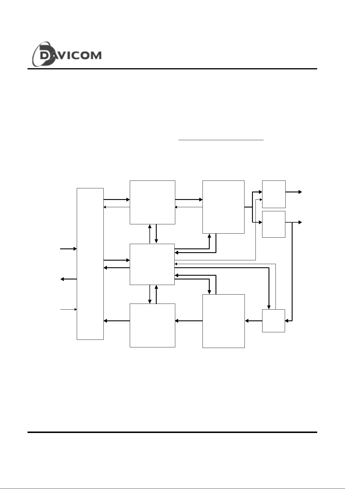
Functional D escrip tion
The DM9801 is a single-chip Home Phoneline Network
transceiver .The DM9801 pr ovides an IEEE 802.3u
subset Media Independent Interface (MII) or a pseudostandard General Purpose Serial Interface (GPSI).
Encoder
Muxed
GPSI or MII
Interface
Master PHY
Controller
Decoder
RLL25
RLL25
The DM9801 enables home networking by allowing
Ethernet packets to be transported over common home
telephone wiring with no modifications, using Ethernet
CSMA/CD media access control procedures as defined in
the IEEE 802.3 standard. Figure 1 sho ws the major
functional blocks implemented in the DM9801.
Transmit
Timing
Generator
HN Drivers
Receiver AFE
Receiver
and
Digital PLL
Figure 1
MII Interface
The DM9801 provides a subset Media Independent
Interface (MII) or a pseudo-standard General Purpose
Serial Interface (GPSI). The MII interface provides a
simple, easy way to implement connection between the
MAC Reconciliation layer and the DM9801 transceiver.
The MII is designed to make the differences between
various media transparent to the MAC sublayer.
The MII consists of a nibble wide receive data bus, a
nibble wide transmit data bus, and control signals to
facilitate data transfers between the PHY and the
Reconciliation layer.
10 Preliminary
TXD (transmit data) is a nibble (4 bits) of da ta that are
driven by the reconciliation sublayer synchronously with
respect to TX_CLK. For each TX_CLK period, which
TX_EN is asserted, TXD (3:0) are accepted for
transmission by the PHY.
TX_CLK (trans mit clock) o utput to the MAC r econciliatio n
sublayer is a clock that provides the timing reference for
the transfer of the TX_EN, TXD, and TX_ER signals.
TX_EN (transmit enable) input from the MAC
reconciliation sublayer to indicate nibbles are being
presented on the MII for transmission on the physical
medium.
Version: DM9801-DS-P 02
March 20, 2000
Page 11

1M Home Phoneline Netwo rk Physical La yer Si ngle Chip T ranscei ver
MII Interface (continued)
RXD (receive data) is a nibble (4 b its) of data that are
sampled by the reconciliation sublayer synchronously with
respect to RX_CLK. For each RX_CLK period that
RX_DV is asserted, RXD (3:0) are transferred from the
PHY to the MAC reconciliation sublayer.
RX_ CL K ( re cei ve clo ck ) o u tp ut t o t he MAC re co n cili a tio n
sublayer is a clock that provides the timing reference for
the transfer of the RX_DV, RXD, and RX_ER signals.
RX_DV (receive data v alid) input from the PHY to indicate
the PHY is presenting recovered and decoded nibbles to
the MAC reconciliation sublayer. To interpret a receive
frame correctly by the reconciliation sublayer, RX _DV
must encompass the frame starting no later than the Startof-Frame delimiter and excluding any End-Stream
delimiter.
DM9801
The DM9801 management functions correspond to
MII specification for IEEE 802.3u-1995 (Clause 22)
for registers 0 through 6 with vendor-specific
registers 16 through 31.
In read/write operation, the management data frame
is 64-bits l ong and starts with 32 contiguous l o gi c
one bits (preamble) synchronization clock cycles on
MDC. The Start of Fram e Delimiter (SFD) is
indicated by a <01> pattern followed by the
operation code (OP):<10> indicates Read operation
and <01> indicates Write operation. For read
operation, a 2-bit turnaround (TA) filin g between
Register Address field and Data field is provided for
MDIO to avoid contention. Following the turnaround
time, 16-bit data is read from or written to the
management regi ster s.
CRS ( ca rr ie r s e ns e) is as s ert ed by t h e PH Y when ei t her
the transmit or receive medium is non-idle and deasserted
by the PHY when the transmit and receive medium are
idle .
MII Ser ia l Management
The MII serial management interface consists of a
data interface, basic register set, and a serial
management interface to the register set. Through
this interface it is possible to control and configure
multiple PHY devices, get status and error
information, and determine the type and capabilities
of the attached PHY device(s).
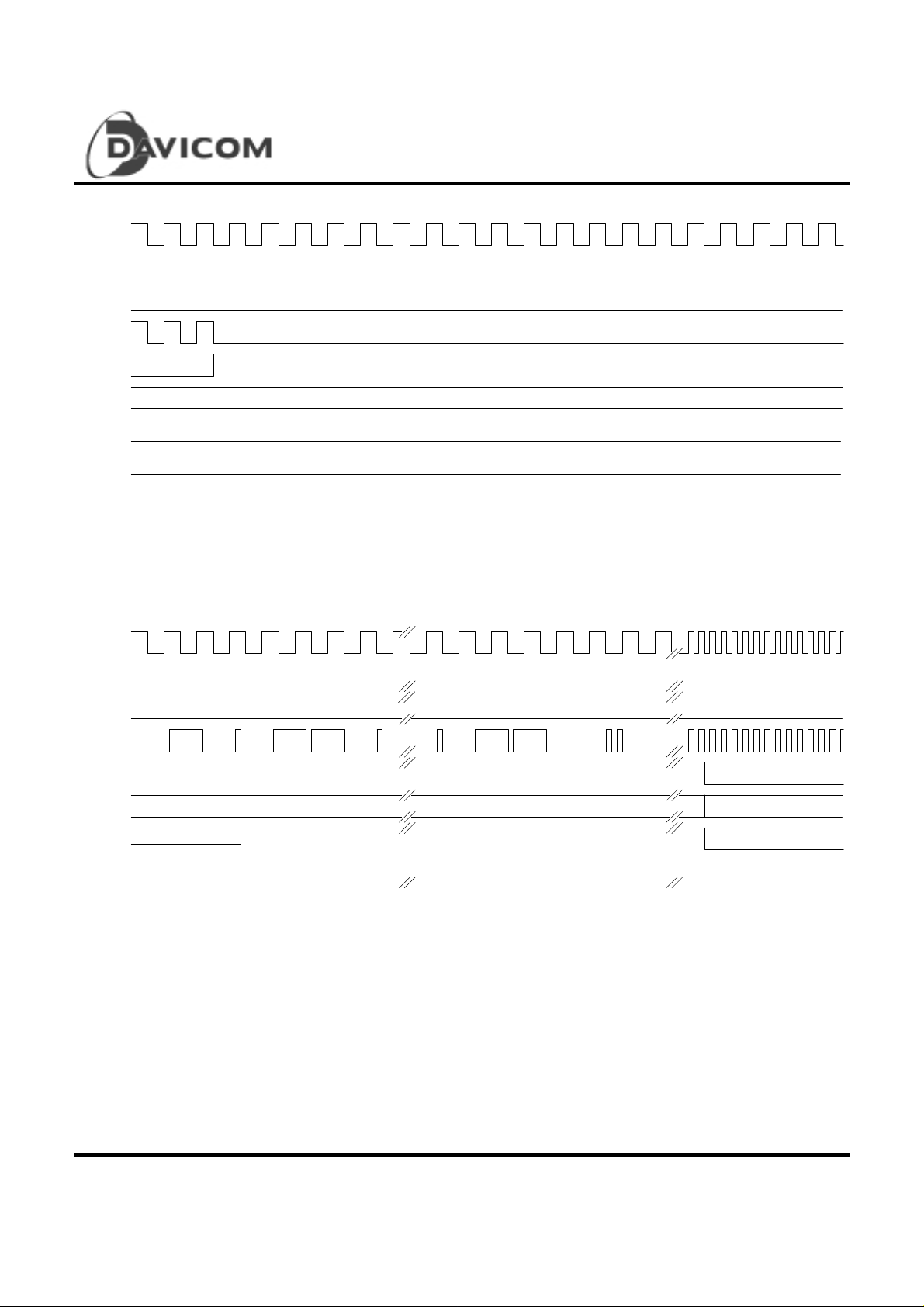
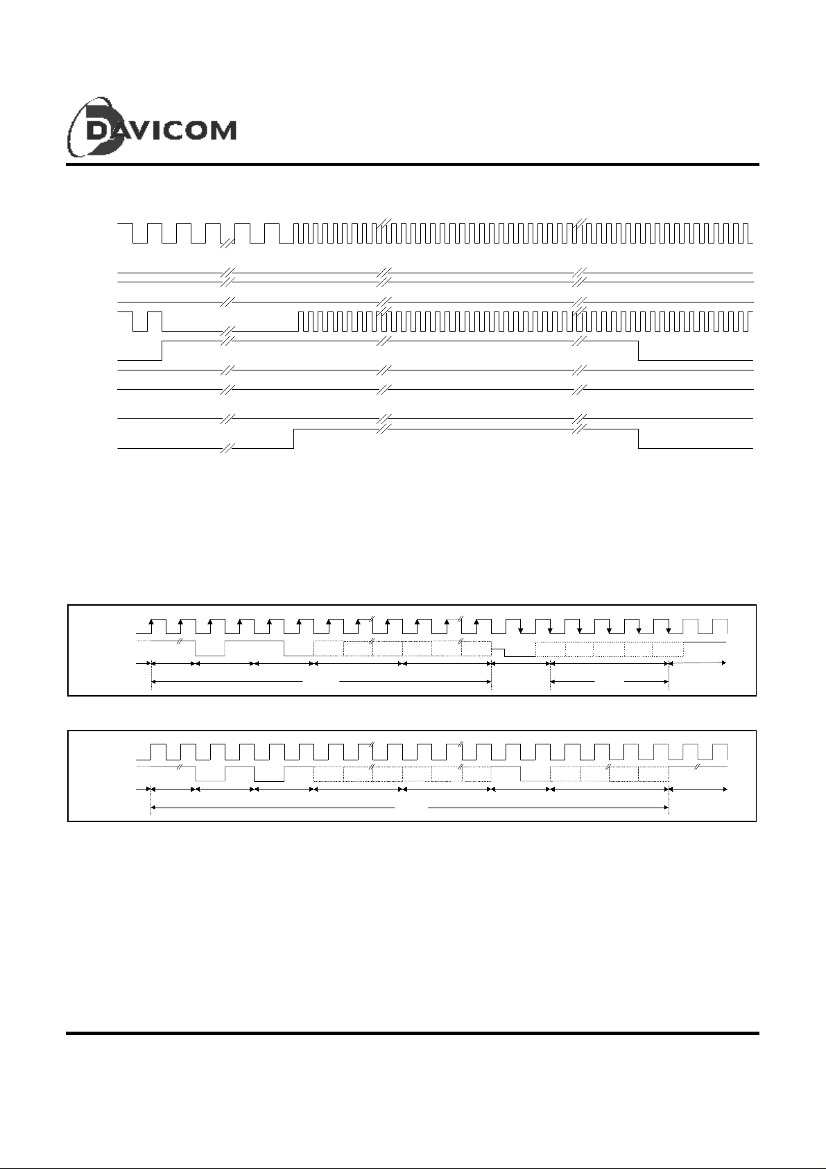
MII Inte rfa ce Transmi t and Re c eive Timing Diagram
TX_CLK
TX_EN
TXD
RX_CLK
CRS
Serial Management Interface
The serial control interface uses a simple two-wired
serial interface to obtain and control the status of
the physical layer through the MII interface. The
serial control interface consists of MDC
(Management Data Clock), and MDI/O
(Management Data Input/Output) signals.
The MDIO pin is bi-directional and may be shared
by up to 32 devices.
0
RXD
RX_DV
COL
0
RX_CLK and TX_CLK are synchronized. All signals are inactive. The period of the two clock is 2333.3 ns.
Idle S tate
Figure 2
Preliminary 11
Version: DM9801-DS-P 02
March 20, 2000
Page 12
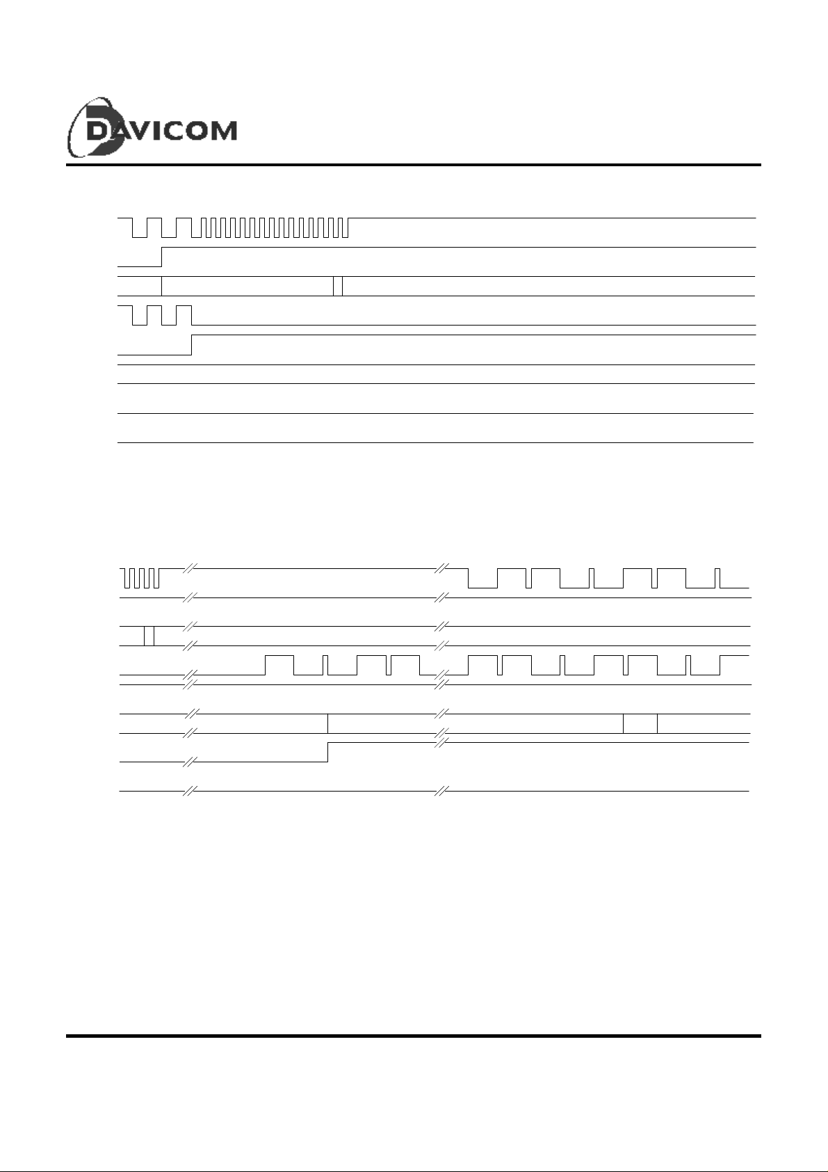
1M Home Phoneli ne Network P hysi cal Layer Si ngle Chi p Transcei ver
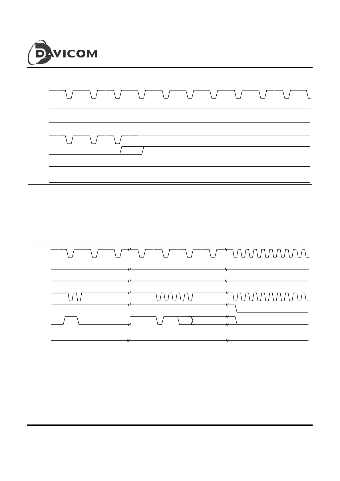
MII Inte rfa ce Transmi t and Re c eive Timing Diagram (continued)
TX_CLK
TX_EN
DM9801
TXD
RX_CLK
CRS
RXD
RX_DV
COL
0
0
RX_CLK becomes disabled (and left in the low state) as soon as CRS is asserted. The clock is re-enabled about 140 u S into
the pac k et.
RXPKT – CRS Asserted
Figure 3
TX_CLK
TX_EN
TXD
RX_CLK
000
CRS
RXD
RX_DV
COL
0
5 (Pream bl e)
DATA 0
RX_CLK and TX_CLK are unrelated to each other during this time. When a symbol has been received and decoded,
RX_CLK toggles at various frequencies depending on what data have been received. Once CRS falls, RX_CLK and
TX_CLK are toggled continuously at 933.3 ns for 22 cycles, after which DM9801 returns to the Idle State.
RXPKT – RX_CLK Active and CRS Cleared
Figure 4
12 Preliminary
Version: DM9801-DS-P 02
March 20, 2000
Page 13
1M Home Phoneline Netwo rk Physical La yer Si ngle Chip T ranscei ver
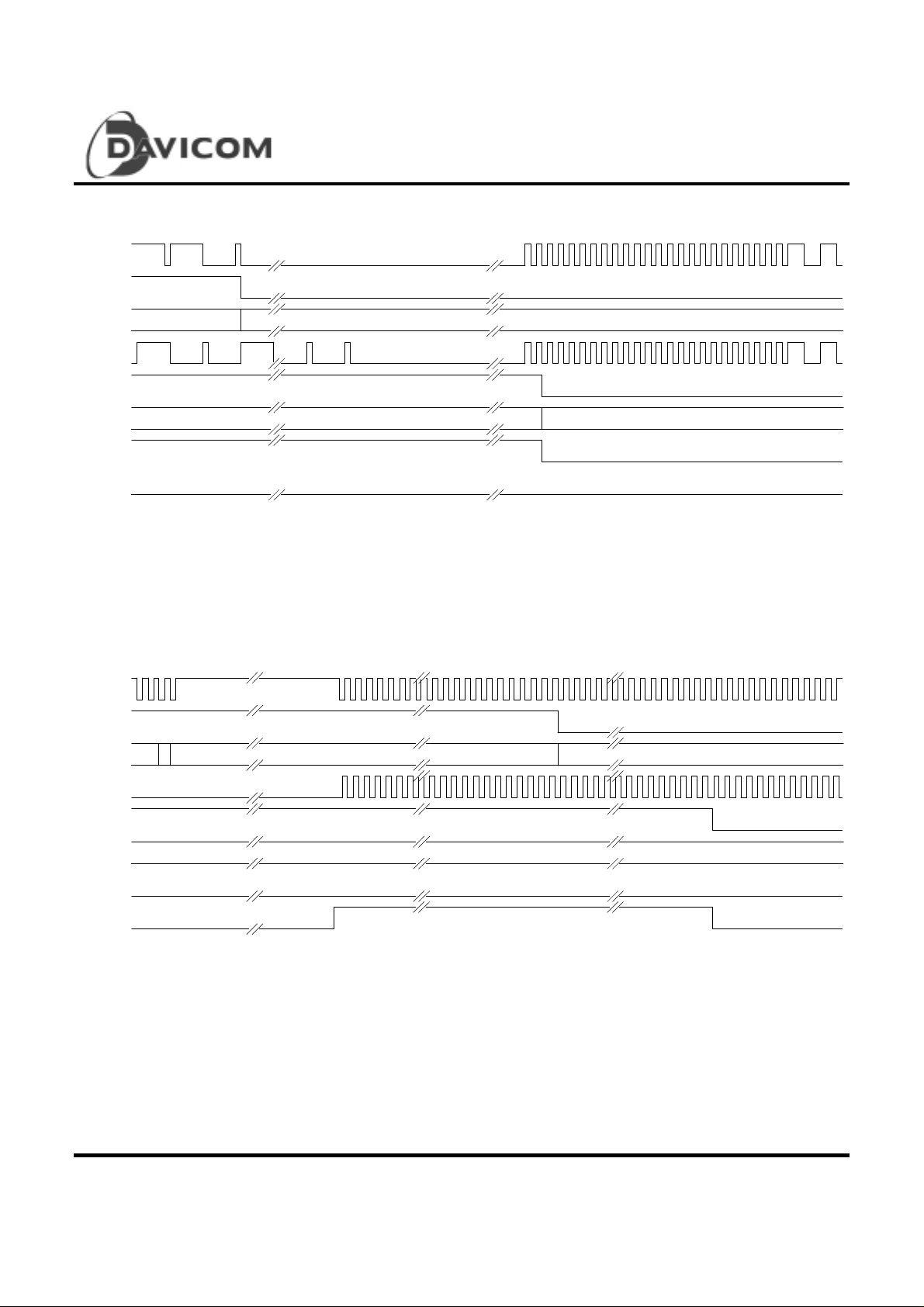
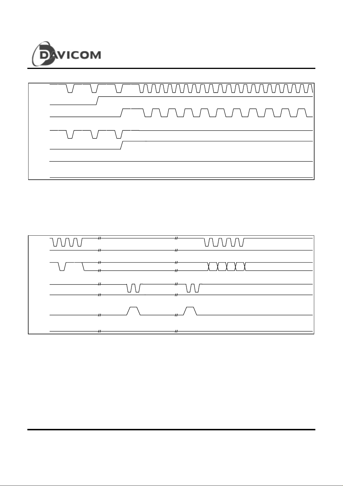
MII Inte rfa ce Transmi t and Re c eive Timing Diagram (continued)
TX_CLK
TX_EN
DM9801
TXD
RX_CLK
CRS
RXD
RX_DV
COL
0
5 (Pream bl e)
D
0
DATA
Once TX_EN is asserted, DM9801 stops RX_CLK, asserts CRS, and toggles TX_CLK at 933.3 ns.
TXPKT – TX_EN Asserted
Figure 5
TX_CLK
TX_EN
D DATA
TXD
RX_CLK
5
CRS
RXD
RX_DV
COL
0
5 (Preambl e)
D
DATA
TX_CLK continues to toggle at 933.3 n s until t he SF D is observed, as shown in the first section of the above diagram. At this
point, TX_CLK is disabled (high) until AID header has been transmitted on the wire (or until a COL has been detected). This
takes about 120 us, at which time RX_CLK starts toggling, thereby shifting 32 bits of preamble and SF D ba ck to t he M AC.
Sometime later, the TX_CLK restarts a s symbols get sent onto the wire in an analogous manner as RX_CLK during packet
reception.
TXPKT – R X_C LK A ct ive
Figure 6
Preliminary 13
Version: DM9801-DS-P 02
March 20, 2000
Page 14
1M Home Phoneli ne Network P hysi cal Layer Si ngle Chi p Transcei ver
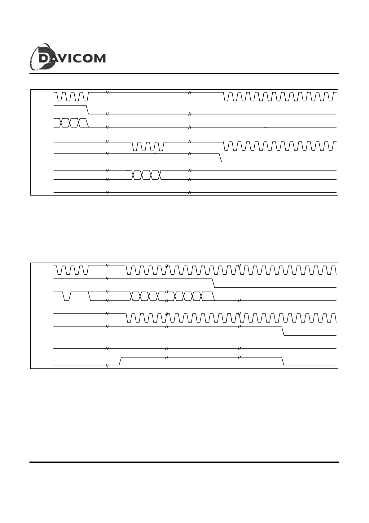
MII Inte rfa ce Transmi t and Re c eive Timing Diagram (continued)
TX_CLK
TX_EN
DM9801
TXD
RX_CLK
CRS
RXD
RX_DV
COL
DATA
DATA
0
0
Once TX_EN is cleared, the last symbol gets encoded and tr an sm itt ed , th e looped-back data is presented back to the MAC,
and CRS falls. Once CRS falls, TX_CLK and RX_CLK toggles with a period of 933.3 ns for 22 c locks, after which the system
returns to the Idle S tate .
TXPKT – TX_EN Cleared
Figure 7
TX_CLK
TX_EN
D DATA 0
TXD
5
RX_CLK
CRS
RXD
RX_DV
COL
0
0
COL will be asserted sometime after the preamble and SFD have been clocked in. TX_CLK and RX_CLK are then clocked
with a period 933.3 ns until CRS d rops. TX_EN drops sometime after COL was asserted. CRS and COL are dropped after
more tha n 80 cloc ks . TX_C LK and RX _CLK keep togg ling at 933. 3 ns period for roughly another 25 clock cycles, when the
system returns to the Idle State.
TXPKT – COL Asserted
Figure 8
14 Preliminary
Version: DM9801-DS-P 02
March 20, 2000
Page 15
1M Home Phoneline Netwo rk Physical La yer Si ngle Chip T ranscei ver
MII Inte rfa ce Transmi t and Re c eive Timing Diagram (continued)
TX_CLK
TX_EN
DM9801
TXD
RX_CLK
CRS
RXD
RX_DV
COL
0
00
0
COL may be asserted up to 120 us after CRS has been asserted. Once COL has been asserted, TX_CLK and RX_CLK run
at a period of 933.3 ns until COL and CRS are cleared. It can take up to about 600 us for CRS to clear.
RXPKT – COL Asserted
Figure 9
Management Interface - Read Frame Structure
MDC
MDIO Read
32 "1"s
Idle Preamble SFD Op Code PHY Address Register Address Turn Around Data Idle
0110A4A3A0R4R3R0
Write
Z
0
D15 D14 D1 D0
//
Read
//
Management Interface - Write Frame Structure
MDC
MDIO Write
32 "1"s 0 1 10 A4 A3 A0 R4 R3 R0 1 0 D15 D14 D1 D0
Idle Preamble SFD Op Code PHY Address Register Address Turn Around Data Idle
Write
Figure 10
Preliminary 15
Version: DM9801-DS-P 02
March 20, 2000
Page 16

1M Home Phoneli ne Network P hysi cal Layer Si ngle Chi p Transcei ver
General Purpose Serial Interface
The DM 9801 provides a subset Media Independent
Interface (MII) or a pseudo-standard General Purpose
Serial In te rface ( GPS I). The GPS I inte r face pr o vides a
simple, easy way to implement connection between the
MAC Reconciliation layer and the DM9801 transceiver.
The GPSI is designed to make the differences between
various media transparent to the MAC sublayer.
The GPSI interface provides a serial receive d ata bus, a
seria l trans mit dat a bu s, a nd control signals to faci litate
data transfers between the DM9801 transceiver and the
Reconciliation layer. The seven signals which comprise
the GPSI are STXDAT, STDCLK, STXEN, SRXDAT,
SRXCLK, CLSN, and CRS. Of these, only STXEN and
STXDAT are inputs to the DM9801, the other five are
outputs from the DM9801.
DM9801
STXEN (serial transmit enable) input from the MAC
reconciliation sublayer to indicate serial data is being
prese nted on the GPSI for transmissio n o n the phy sical
medium.
SRXDAT (serial receive data) is a serial stream of data
that is sampled by the reconciliation s ublayer
synchronously with respect to SRXCLK.
SRXCLK (serial receive data clock) is an output to the
MAC reconciliation sublayer. SRDCLK is a clock that
provides the timing reference for the transfer of the
SRXDAT in GPSI mode.
CLSN (c ol lision dete ct) is an o utput to t he MAC
re c o n c il ia tio n su b layer. CLSN is asserted high to
indicate detection of collision condition
STXDAT (serial transmit data) is a serial stream of data
that are driven by the reconciliation sublayer
synchronously with respect to STDCLK. For each
STDCLK period, which STXEN is asserted, STXDAT is
accepted for transmission by the PHY.
STDCLK (s er ial tran s mit d a ta c loc k) is a n o utput to the
MAC reconciliation sublayer. STDCLK is a clock that
provides the timing reference for the transfer of the
STXDAT in GPSI mode.
STDCLK
STXEN
STXDAT
SRDCLK
CRS
CRS (carrier sense) is an output to the MAC reconciliation
sub layer that is asserted high to indicate the
presence of carrier due to receive or transmit
activities.
The subsequent sections analyze each GPSI related state
of the DM9801 in detail.
SRXDAT
CLSN
SRDCLK and STDCLK are synchronized. All other signals are inactive.
Idle S tate
Figure 11
16 Preliminary
Version: DM9801-DS-P 02
March 20, 2000
Page 17
1M Home Phoneline Netwo rk Physical La yer Si ngle Chip T ranscei ver
General Purpose Serial Interface (continued)
STDCLK
STXEN
STXDAT
SRDCLK
CRS
SRXDAT
CLSN
SRDCLK becomes disabled as soon as CRS is asserted.
RXPKT- CRS Asserted
DM9801
Figure 12
STDCLK
STXEN
STXDAT
SRDCLK
CRS
SRXDAT
CLSN
SRDCLK and STDCLK are unrelated to each other during this time. When a symbol has been received and decoded,
SRDCLK toggles in order to shift out the three to six bits encoded in the symbol. The middle portion of this diagram shows the
end of the preamble, followed by the SFD and the beginning of the datagram. CRS will fall a fter the last received symbol.
Once CRS falls, SRDCLK and STDCLK are toggled continuously for 97 cycles after which the DM9801 returns to the Idle
state.
RXPKT - SRDCLK Active and CRS Cleared
Figure 13
Preliminary 17
Version: DM9801-DS-P 02
March 20, 2000
Page 18
DM9801
1M Home Phoneli ne Network P hysi cal Layer Si ngle Chi p Transcei ver
General Purpose Serial Interface (continued)
STDCLK
STXEN
STXDAT
SRDCLK
CRS
SRXDAT
CLSN
Once STXEN is asserted, the DM9801 stops SRDCLK, asserts CRS, and toggles STDCLK.
TXPKT - STXEN Asserted
Figure 14
STDCLK
STXEN
STXDAT
SRDCLK
CRS
SRXDAT
CLSN
STDCLK continues to toggle until SFD is observed, as shown in the first section on the abo ve diagram. At this point, STDCLK
is disabled until the AID header has been transmitted on the wire or until CLS has been de tect e d . At th is tim e SRDCLK starts
toggling, thereby shifting 32 bits of preamble and SFD back to the MAC. Sometime later, the STDCLK restarts as symbols get
sent onto the wire in an analogous manner as SRDCLK during packet reception.
TXPKT - SR DCLK Ac tive
Figure 15
18 Preliminary
Version: DM9801-DS-P 02
March 20, 2000
Page 19
DM9801
1M Home Phoneline Netwo rk Physical La yer Si ngle Chip T ranscei ver
General Purpose Serial Interface (continued)
STDCLK
STXEN
STXDAT
SRDCLK
CRS
SRXDAT
CLSN
Once STXEN is cleared, the last symbol gets encoded and transmitted. The looped-back data is presented back to the MAC
and sometime later CRS falls. Once CRS falls, STDCLK and SRDCLK toggl e for 97 clocks after which the sy stem return s to
the Idle state.
TXPKT - STXEN Cleared
Figure 16
STDCLK
STXEN
STXDAT
SRDCLK
CRS
SRXDAT
CLSN
CLSN will be asserted some time after the preamble and SFD ha ve been clock ed in. STDCLK and SRDCLK are then clocked
until CRS drops. STXEN drops s ometime after CLSN was as serted. CRS and CLSN are dropped togeth er after more than
500 clocks. STDCLK and SRDCLK keep toggling for approximately another 100 clock cycles, then the system returns to the
idle sta te .
TXPKT - CLSN Asserted
Figure 17
Preliminary 19
Version: DM9801-DS-P 02
March 20, 2000
Page 20

DM9801
1M Home Phoneli ne Network P hysi cal Layer Si ngle Chi p Transcei ver
General Purpose Serial Interface (continued)
STDCLK
STXEN
STXDAT
SRDCLK
CRS
SRXDAT
CLSN
CLSN may be asserted up to 120us af ter CRS has been asserted. O nce CLSN has been asserted STDCLK and SRDCLK
run at a period of 233.3ns per cycle until 97 cycles after CLSN and CRS are cleared. It can take up to about 60us for CRS to
clear.
RXPKT - C LSN Clea re d
Figure 18
20 Preliminary
Version: DM9801-DS-P 02
March 20, 2000
Page 21

1M Home Phoneline Netwo rk Physical La yer Si ngle Chip T ranscei ver
Serial Peri phera l Interf ac e (SPI) Bus
When INTFSEL is asserted, t he DM9801 is
configured to operate i n SPI mode. While
configured to operate in SPI mode, the DM9801 can
act as a SPI Slave or SPI Master. Asserting
SMODE places the DM9801 in SPI Slave mode.
Clearing SMODE places the DM9801 in SPI Master
Mode.
The SPI (Serial Peripheral Interface) Bus uses a
four-wired serial interface to obtain and control the
status of the physical layer through the SPI Bus
interfac e. T he seri al cont r ol interface consists of SI
(serial data input), SO (serial dat a output ) , SCLK
(serial cl oc k ), and SCS# (serial i nterface chip
select) signals. When operating in Master mode the
DM9801 drives the SCLK and SCS# signals, when
operating in Slave mode these signals are inputs.
SPI-Slave Mode (Valid only in GPSI Mode)
When SMODE is asserted the DM9801 is
configured for SPI Slave operation. Commands are
issued to the DM9801 by asserting the SCS#
signal, shifting in an 8-bit opcode followed by a
register address and an end delimiter. If the
operation is a write, the address is followed by an 8-
DM9801
bit data byte. If the operation is a read, the SO pin
will shift out an 8-bit data byte representing the
contents of the register referenced by the address
field. Only one command can be sent in one SCS#
cycle. The D M9801 does not support multiple byte reads
or writes.
SPI-Mast er Mode (Valid only in GPSI Mode)
When SMODE is cleared the DM9801 is configured
for SPI Master operation. When the DM9801 is
configured for SPI-Master operation, it will load all
programmable registers from an external SPI type
EEPROM. The memory locations loaded may be
offset via the boot page pins, BP[1:0], allowing a
single 256 byte serial EEPROM to hold four distinct
sets of default register values.
After RESET# has cleared the DM9801 will assert
SCS#, shift out a Read opcode (0x03), followed by
the initial address to be read (as modified by the
Boot Page pins). The DM9801 will then shift in the
memory contents, auto incrementing the register
address being programmed every 8-bits. Once all
64-bytes have been read, the DM9801 releases
SCS#. The SCLK conti nues to run. Opcodes are
shown in Table 1.
Instruction Format Instruction Name
0000 0110 Set WE
0000 0100 Clear WE
0000 0011 Read
0000 0010 Write
OPCODE S
Table 1
Preliminary 21
Version: DM9801-DS-P 02
March 20, 2000
Page 22

1M Home Phoneli ne Network P hysi cal Layer Si ngle Chi p Transcei ver
Serial Peripheral Interface (SPI) Bus (continued)
SCLK
SCS#
DM9801
SO
SI
SCLK
SCS#
SI
SO
b7 b6
Instruction Byte Address Byte
b7 b6 b5 b4 b3 b2 b1 b0 b7 b6 b5
Data Byte 0
SPI Master Mode Timing
Figure 19
b7 b6 b5 b4 b3 b2 b1 b0 b7 b6 b5 b4 b3 b2 b1 b0 b7 b6 b5 b4 b3 b2 b1 b0 b7 b6 b5
Instruction Byte Address Byte Data Byte
b7 b6 b5 b4 b3 b2 b1 b0 b7 b6 b5
Data Byte
(Don't care on read)
(High-Z when writing)
SPI Slave Mode Timing
Figure 20
22 Preliminary
Version: DM9801-DS-P 02
March 20, 2000
Page 23

DM9801
1M Home Phoneline Netwo rk Physical La yer Si ngle Chip T ranscei ver
MII Ser ial Mana geme nt Re gister Map ( INTFS EL = 0, M II Mo de)
Register
Address
0 BMCR RW 0x0000 Basic Mode Control Register (valid only when MII
1 BMSR RO 0x0820 Basic Mode Status Register (valid only when MII
2 PHYIDR1 RO 0x0181 PHY Identifier Register #1 (valid only when MII Emulati on
3 PHYIDR2 RO 0xB900 PHY Identifier Register #2 (valid only when MII Emulation
4 ANAR RO 0x0021 Auto-negotiation Advertisement Register (valid only when
5 ANLPAR RO 0x0000 Auto-negotiation Link Partner Ability Register (valid only
6 ANER RO 0x0000 Auto-Negotiation Expansion Register (valid only when MII
7-15 Not Used Tri-State Reserved
16 CNTRL RW 0x 0005 Control Register
17 STATUS RW 0x0000 S tatus Register
18 IMASK RW 0x0000 Interrupt Mask Register
19 IS TAT RW 0x0000 Interrupt Status Register
20 TX_PCOM_HI RW 0x0000 Transmit PHY Communication Hi Word
21 TX_PCO M _LO RW 0x0000 Transmit PHY Communication Lo Word
22 RX_PCOM_HI RW 0x0000 Receive PHY Communication Hi Word
23 RX_PCOM_LO RW 0x0000 Receive PHY Communication Lo Word
24 PEAK_NOISE RW 0xFF04 Peak Level and Noise Level Register
25 NOISE_CNTRL_A RW 0x8007 Noise Ceiling and Noise Floor Register
26 NOISE_CNTRL_B RW 0x00F4 Noise Events and Noise Attack Register
27 FWENA RW 0x0000 Four Wire Enable and Disable Link Register
28 AID_ADDRESS RW 0x0000 AID Address Register
29 AID_CNTRL RW 0x4014 AID Interval and AID ISBI Register
30 SYM_CNTRL RW 0x1C2C DATA ISBI Control Register
31 TX_SIG_CNTRL RW 0x4404 Transmit Pulse Control Register
Register Name Access
Type
Default
Value
Description
Emulation Support is enabled, Config1 = 1).
Emulation Support is enabled, Config1 = 1).
Support is enabl ed, Config1 = 1).
Support is enabl ed, Config1 = 1).
MII Emulation Support i s enabl ed, Config1 = 1).
when MII Emulation Support is enabled, Config1 = 1) .
Emulation Support is enabled, Config1 = 1).
Key to Defa ult
In the register description that follows, the default column
takes the for m:
<Reset Value>, <Access Type> / <Attribute(s)>
Where
<Reset Value>:
1 Bit set to logic one
0 Bit set to logic zero
X No default value
(PIN#) Value latched in from pin # at reset
Preliminary 23
Version: DM9801-DS-P 02
March 20, 2000
<Access Type>:
RO = Read onl y
RW = Read/Write
<Attribute (s)>:
SC = Self clearing
P = Value permanently set
LL = Latching low
LH = Latching high
Page 24

1M Home Phoneli ne Network P hysi cal Layer Si ngle Chi p Transcei ver
Basic Mode Control Register (BMCR) - Register 0
Bit Bit Name Default Description
0.15 Reset 0, RW/SC
0.14 Loopbac k 0, RW
0.13 Speed Selection 0, RO/P
0.12 Auto-negotiation
Enable
0.11 Power Down 0,RW
0.10 Isolate 0,RW
0.9 Restart Autonegotiation
0.8 Duplex Mode 0,RO/P
0.7 Collision Test 0,RO/P
0.6-0.0 Reserved 0,RO
0,RO/P
0,RO/P
Reset:
1=Software res e t
0=Normal operation
When set this bit c onfigures the PHY status and control
registers to thei r default states. This bit will return a value of
one until the reset process is complete
Loopback:
Loopback control register
1=Loopback enabled
0=Normal operation
Speed Select:
The DM9801 does not support this function. This bit is
permanently set t o 0
Auto-negotiation Enable:
The DM9801 does not support this function. This bit is
permanently set t o 0
Power Down:
1=Power down enabled
0=Normal operation
Setting this bit will power down the DM9801 with the exception
of the crystal oscill ator circuit.
Isolate:
1= Isolate
0= Normal Operation
When this bit is set the data path will be isolated from the MII
interfac e. T X_CLK, RX_CLK, RX_DV, RXD[3:0] , COL and CRS
will be placed in a high impedance state. The management
interfac e is not effected by this bit. When the PHY address is
set to 00000 the isolate bit will be set upon power-up/reset.
Restart Auto-negotiation:
The DM9801 does not support this function. This bit is
permanently set t o 0
Duplex Mode:
The DM9801 does not support this function. This bit is
permanently set t o 0
Collisi on Te s t :
The DM9801 does not support this function. This bit is
permanently set t o 0
Reserved:
Write as 0, ignore on read
DM9801
24 Preliminary
Version: DM9801-DS-P 02
March 20, 2000
Page 25

1M Home Phoneline Netwo rk Physical La yer Si ngle Chip T ranscei ver
Basic Mode Status Register (BMSR) - Register 1
Bit Bit Name Default Description
1.15 100Base-T4 0,RO/P
1.14 100Base-TX
Full Duplex
1.13 100Base-TX
Half Duplex
1.12 10Base-T
Full Duplex
1.11 10Base-T
Half Duplex
1.10-1.7 Reserved 0,RO
1.6 MF Preamble
Suppression
1.5 Auto-negotiation
Complete
1.4 Remote Fault 0,RO/P
1.3 Auto-negotiation
Ability
1.2 Link Status 0,RO/LL
1.1 Jabber Detect 0,RO/P
1.0 Extended
Capability
0,RO/P
0,RO/P
0,RO/P
1,RO/P
0,RO/P
1,RO/P
0,RO/P
0,RO/P
Reserved:
The DM9801 does not support this function. This bit is
permanently set t o 0
Reserved:
The DM9801 does not support this function. This bit is
permanently set t o 0
Reserved:
The DM9801 does not support this function. This bit is
permanently set t o 0
Reserved:
The DM9801 does not support this function. This bit is
permanently set t o 0
Reserved:
The DM9801 supports half Duplex Operation only. This bit is
permanently set t o 1
Reserved:
Write as 0, ignore on read
MII Frame Preamble Suppression:
1=PHY will accept management frames with preamble suppressed
0=PHY will not accept management frames with preamble suppressed
Auto-negotiat ion Com plete:
The DM9801 does not support this function. This bit is
permanently set t o 1
Remote Fault:
The DM9801 does not support this function. This bit is
permanently set t o 0
Auto C onf igur at io n A bil ity:
The DM9801 does not support this function. This bit is
permanently set t o 0
Link S tatus :
1=Valid link established
0=Link not established
The link status bit is implemented with a latching function, so that the
occurrence of a link failure condition causes the Link Status bit to be
cleared and remain cleared until it is read via t he management
inter f a ce
Jabber Detect:
The DM9801 does not support this function. This bit is
permanently set t o 0
Exten ded Ca pabi lity:
The DM9801 does not support this function. This bit is
permanently set t o 0
DM9801
PHY ID Identifier Register #1 (PHYIDR1) - Register 2
The PHY Identifier Registers #1 and #2 work together in a single identifier of the DM9801. The Identifier consists of a
concatenation of the Organizati ona lly Un ique I dent if ier (OUI), a vendor's model number, and a model revision number.
DAVICOM Semiconductor's IEEE assigned OUI is 00606E.
Preliminary 25
Version: DM9801-DS-P 02
March 20, 2000
Page 26

DM9801
1M Home Phoneli ne Network P hysi cal Layer Si ngle Chi p Transcei ver
Bit Bit Name Default Description
2.15-2.0 OUI_MSB <0181H>
PHY Identifier Register #2 (PHYIDR2) - Register 3
Bit Bit Name Default Description
3.15-3.10 OUI_LSB <101110>,RO/P
3.9-3.4 VNDR_MDL <010000>,RO/P
3.3-3.0 MDL_REV <0000>,RO/P
Auto-negotiation Advertisement Register(ANAR) - Register 4
This register contains the advertised abilities of the DM9801 device as they will be transmitted to link partners during Autonegotiation.
Bit Bit Name Default Description
4.15 NP 0,RO/P
4.14 ACK 0,RO/P
4.13 RF 0, RO/P
4.12-4.11 Reserved 0, RO
4.10 FCS 0, RO/P
4.9 T4 0, RO/P
4.8 TX_FDX 0, RO/P
4.7 TX_HDX 0, RO/P
OUI Most Significant Bits:
This register stores bi ts 3 - 18 of the OUI (00606E) t o bits 15 0 of this register respectively. The most significant two bits of
the OUI are ignored (the IEEE standard refers to these as bit 1
and 2)
OUI Least Significant Bits:
Bits 19 - 24 of the OUI (00606E) are mapped to bits 15 - 10 of
this register respe ctively
Vendor Model Number:
Six bits of the vendor model number mapped to bits 9 - 4 (most
significant bit to bit 9)
Model Revision Number:
Four bits of t he vendor m odel revision number mapped to bits 3
- 0 (most significant bit to bit 3)
Next Page Indication:
The DM9801 does not support the next page function. This bit
is permanentl y set to 0
Acknowledge:
1=Link partner ability data reception acknowledged
0=Not acknowledged
The DM9801's state machine will automatically control this bit.
Software should not attempt to write to this bit.
Remote Fault:
The DM9801 does not support this function. This bit is
permanently set t o 0
Reserved:
Write as 0, ignore on read
Flow Control S upport:
The DM9801 does not support this function. This bit is
permanently set t o 0
100Base-T4 Support:
The DM9801 does not support this function. This bit is
permanently set t o 0
100Base-TX Full Duplex Support:
The DM9801 does not support this function. This bit is
permanently set t o 0
100Base-TX Support:
The DM9801 does not support this function. This bit is
permanently set t o 0
26 Preliminary
Version: DM9801-DS-P 02
March 20, 2000
Page 27

1M Home Phoneline Netwo rk Physical La yer Si ngle Chip T ranscei ver
Auto-negotiation Advertisement Register(ANAR) - Register 4 (continued)
Bit Bit Name Default Description
4.6 10_FDX 0, RO/P
4.5 10_HDX 1, RO/P
4.4-4.0 Selector <00001> , RO/P
Auto-negotiation Link Partner Ability Register (ANLPAR) - Register 5
This register contains the advertised abilities of the link partner as t hey are received during Auto-negotiation.
Bit Bit Name Default Description
5.15 NP 0, RO/ P
5.14 ACK 0, RO/P
5.13 RF 0, RO/P
5.12-5.10 Reserv ed 0, RO
5.9 T4 0, RO/P
5.8 TX_FDX 0, RO/P
5.7 TX_HDX 0, RO/P
5.6 10_FDX 0, RO/P
5.5 10_HDX 0, RO
5.4-5.0 Selector < 00000>, RO
10Base-T Full Duplex Support:
The DM9801 does not support this function. This bit is
permanently set t o 0
10Base-T Support:
1=10Base-T Half Duplex supported by the link partner
0=10Base-T Half Duplex not supported by the link partne r
Protocol Selection Bits:
These bits contain the binary encoded protocol selector
supported by this node.
<00001> indicates that this device supports IEEE 802.3
CSMA/CD.
Next Page Indication:
0= Link partner, no next page available
1= Link partner, next page available
Acknowledge:
1=Link partner ability data reception acknowledged
0=Not acknowledged
The DM9801's state machine will automatically control this bit.
Software should not attempt to write to this bit.
Remote Fault:
1=Remote fault indicated by link partner
0=No remote fault indicated by link partner
Reserved:
Write as 0, ignore on read
100Base-T4 Support:
The DM9801 does not support this function. This bit is
permanently set t o 0
100Base-TX Full Duplex Support:
The DM9801 does not support this function. This bit is
permanently set t o 0
100Base-TX Support:
The DM9801 does not support this function. This bit is
permanently set t o 0
10Base-T Full Duplex Support:
The DM9801 does not support this function. This bit is
permanently set t o 0
10Base-T Support:
1=10Base-T Half Duplex supported by the link partner
0=10Base-T Half Duplex not supported by the link partne r
Protocol Selection Bits:
Link partner binary encoded protocol selector
DM9801
Preliminary 27
Version: DM9801-DS-P 02
March 20, 2000
Page 28

1M Home Phoneli ne Network P hysi cal Layer Si ngle Chi p Transcei ver
Auto-ne go tiat io n Ex pa nsi on R e giste r (A NER ) - Re gis ter 6
Bit Bit Name Default Description
6.15-6.5 Reserved 0, RO
6.4 PDF 0, RO/P
6.3 LP_NP_ABLE 0, RO/P
6.2 NP_ABLE 0,RO/P
6.1 PAGE_RX 0, RO/P
6.0 LP_AN_ABLE 0, RO/P
Reserved:
Write as 0, ignore on read
Local Device Parallel Detection Fault:
PDF=1: A fault detected via parallel detection function.
PDF=0: No fault detect ed via parallel detec tion function
DM9801 does not support this function, so this bit is always 0.
Link Partner Ne xt Page A ble:
LP_NP_ABLE=1: Link partner, next page available
LP_NP_ABLE=0: Link partner, no next page
DM9801 does not support this function, so this bit is always 0.
Local Device Next Page Able:
NP_ABLE=1: DM9801, next page available
NP_ABLE=0: DM9801, no next page
DM9801 does not support this function, so this bit is always 0.
New Page Received:
A new link code word page received. This bit will be
automatically cleared when the register (Register 6) is read by
management.
DM9801 does not support this function, so this bit is always 0.
Link Partner A ut o-negotiation Able:
LP_AN_ABLE=1 indicates that the link par tner supports Autonegotiation.
DM9801 does not support this function, so this bit is always 0.
DM9801
Control Register - Register 16
Bit Bit Name Default Description
16.15 IG_RMT_CMDS 0,RW
16.14 AVG_PEAK_RL 0,RW
16.13 EN_SHORT_CD 0,RW
16.12 DIS_INC_NOISE 0,RW
16.11 CMD_LO_PWR 0,RW
16.10 CMD_HI_PWR 0,RW
Ignore Remote Commands:
1=Remote commands are ignored
0=Remote commands will be accepted from any node in the
network. The value of the CMDENA pin is latched into this bit at
power-up/reset.
Average Peak Rule:
1= Average peak with measured noise ins t ead of noise + 25%
0= Normal operation
Enable Short CD:
1= Enable short CD noise rule
Do not count bad SYNC if CD is longer than 160uS
0= Normal operation
Disable Increment of Noise:
1= Disable 25% increase of noise slice when in a packet
0= Normal operation
Command Low Pow e r:
1= Transmit power is set to low
0= Normal operation
Remote commands will be issued if this bi t is set
Command High Power:
1= Transmit power is set to high
0= Normal operation
Remote commands will be issued if this bi t is set
28 Preliminary
Version: DM9801-DS-P 02
March 20, 2000
Page 29

1M Home Phoneline Netwo rk Physical La yer Si ngle Chip T ranscei ver
Control Register - Register 16 (continued)
Bit Bit Name Default Description
16.9 CMD_LO_SPD 0,RW
16.8 CMD_HI_SPD 0,RW
16.7 AID_ADR_NEG 0,RW
16.6 CLR_NS_EVNT 0,RW
16.5 SLC_LVL_ADP 0,RW
16.4 PWR_DWN 0,RW
16.3 Reserved 0,R W
16.2 S peed 1, RW
16.1 Power 0, RW
16.0 Reserved 1,R W
Command Low Speed:
1= Transmit speed is set to low
0= Normal operation
Remote commands will be issued if this bi t is set
Command High S pe ed:
1= Transmit speed is set to high
0= Normal operation
Remote commands will be issued if this bi t is set
AID Address Negotiation:
1= Stop AID address negotiation
0= Normal operation
Clear Noise Event Register:
1= Clear the Noise Event Register
0= Normal operation
Slice Level Adaptation:
1= Slice level adaptation is disabled (stopped).
0= Slice level adaptation is enabled
Power Down:
Writing a 1 to this bit will cause DM9801 to enter Sleep mode
and power down all circuits except the oscillator and clock
generator cir c uit. To exit Sleep mode, write 0 to this bit position.
The prior configuration will be retained when th e sleep state is
terminated, but the state machine will be reset
Reserved:
This bit m ust be written as 0
Speed:
1= high speed
0= low speed
This bit indicates the network speed is set to high as selected
by the status of the SPDSEL pin during power-up/reset.
Power:
1= high power
0= low power
This bit indicates the network power is set to high as selected
by the status of the PWRSEL pin during power-up/reset.
Reserved:
This bit m ust be written as 1
DM9801
Preliminary 29
Version: DM9801-DS-P 02
March 20, 2000
Page 30

1M Home Phoneli ne Network P hysi cal Layer Si ngle Chi p Transcei ver
Status Register - Register 17
Bit Bit Name Default Description
17.15 –
17.11
17.10 LINK_STA 0, RO
17.9 DIS_LED_ST R 0, RW
17.8 –
17.7
17.6 R X_PWR 0, R O
17.5 RX_SPD 0, RO
17.4 RX_VER 0, RO
17.3 -
17.0
Reserved 0, RW
Reserved 0, RW
Reserved 0, RW
Reserved:
Write as 0, ignore on read
Link Sta tus:
This bit reports the Link Status of the DM9801
Disable LED Stretchers:
This bit disables LED pulse stretchers
Reserved:
Write as 0, ignore on read
Receive Power:
This bit is an indication of the current rec eiv e signal power.
1= The receive signal power is hi gh.
0= The receive signal power is l ow.
Receive Speed:
This bit is an indication of the current rec eiv e speed.
1= The receive speed is high.
0= The receive speed is low.
Receive Version:
This bit is an indic ation of the current receive version.
1= The receive version is not version 0.
0= The receive version is version 0.
Reserved:
Write as 0, ignore on read
DM9801
IMASK (Interrupt Mask) Register - Register 18
Bit Bit Name Default Description
18.15 –
18.10
18.9 MSK_RX_PCOM 0,RW
18.8 MSK_TX_PCOM 0,RW
18.7 –
18.4
18.3 MSK_PKT_RCV 0,RW
18.2 MSK_PKT_XMIT 0,RW
18.1 MSK_RMT_RCV 0,RW
18.0 MSK_CMD_SNT 0,RW
Software
Interrupts
Reserved 0,RW
0,RW
Software Inter rupts:
1= Software interrupts will not activate the INT# pin
0= Software interrupts will activate the INT# pin
Mask RXPCOM Valid:
1= RX_PCOM_VAL will not activate the INT# pin
0= RX_PCOM_VAL will activate the INT# pin
Mask TXPCOM Ready:
1= TX_PCOM_RDY will not activate the INT# pin
0= TX_PCOM_RDY will activate the INT# pin
Reserved:
Write as 0, ignore on read
Mask Packet Received:
1= Packet Received will not activate the INT# pin
0= Packet Received will activate the INT# pin
Packet Transmitted:
1= Packet Transmitted will not activate the INT# pin
0= Packet Transmitted will activate the INT# pin
Remote Command Received:
1= Remote Command Received will not activate the INT# pin
0= Remote Command Received will activate the INT# pin
Remote Command Sent:
1= Remote Command Sent will not activate the INT# pin
0= Remote Command Sent will activate the INT# pin.
30 Preliminary
Version: DM9801-DS-P 02
March 20, 2000
Page 31

1M Home Phoneline Netwo rk Physical La yer Si ngle Chip T ranscei ver
ISTAT (Interrupt Status) Register - Register 19
This reg ister reports the state of each interrupt source regardless of the state of the IMASK Register.
Bit Bit Name Default Description
19.15 –
19.10
19.9 RX_PCOM_VAL 0,RW
19.8 TX_PCOM_RDY 0,RW
19.7 –
19.4
19.3 PKT_RCVD 0,RW
19.2 PKT_XMITD 0,RW
19.1 RMT_CMD_RCV 0,RW
19.0 RMT_CMD_SNT 0,RW
Software
Interrupts
Reserved 0,RW
0,RW
Software Inter rupts:
When set any bit of those registers indicates software interrupt
is on.
RXPCOM Valid:
When set this bit indicates a non-null RX_PCOM has been
received.
Accessing the high byte of the RX_PCOM register clears this
bit.
TXPCOM Ready:
When set this bit indicates a non-null TX_PCOM has been
loaded into the TX_PCOM register.
Reserved:
Write as 0, ignore on read
Packet Received:
When set this bit indicates a packet has been received
Packet Transmitted:
When set this bit indicates a packet has been transmitted
Remote Command Received:
When set this bit indicates a valid remote command has been
received.
Remote Command Sent:
When set this bit indicates a valid remote command has been
sent.
DM9801
TX_PCOM High Register - Register 20
Bit Bit Name Default Description
20.15 –
20.0
TX_PCOM Low Register - Register 21
Bit Bit Name Default Description
21.15 –
21.0
TX_PCOM_HI 0, RW
TX_PCOM_LO 0, RW
TX_PCOM_HI:
The high order word of the 32-bit transmitted data field to be used for
out-of-band communications between PHY management entities.
The PHY will send all-0 PCOMs until the high byte has been
accessed.
An access of any of the four TX_PCOM bytes will clear the
TX_PCOM_RDY bit in the ISTAT register.
TX_PC OM_ LO:
The low order word of the 32-bit transmitted data field to be used for
out-of-band communications between PHY management entities.
The PHY will send all-0 PCOMs until the high byte in TX_PCOM_HI
has been accessed.
An access of any of the four TX_PCOM bytes will clear t h e
TX_PCOM_RDY bit in the ISTAT register.
Preliminary 31
Version: DM9801-DS-P 02
March 20, 2000
Page 32

1M Home Phoneli ne Network P hysi cal Layer Si ngle Chi p Transcei ver
RX_PCOM High Register - Register 22
Bit Bit Name Default Description
22.15 –
22.0
RX_PCOM Low Register - Register 23
Bit Bit Name Default Description
23.15 –
23.0
RX_PCOM_HI 0, RW
RX_PCOM_LO 0, RW
RX_PCOM_HI:
The high order word of the 32-bit receive data field to be used for outof-band communications between PHY management entities.
A non-null receive PCOM will set the RX_PCOM_VAL bit in the ISTAT
register.
An access of the high byte of t his register will clear the
RX_PCOM_VAL bit in the ISTAT register.
RX_PCOM_LO:
The low ord er w ord o f the 32- b it rec eiv e data field to be us ed f or o u t-ofband communications between PHY management entities.
A non-null receive PCOM will set the RX_PCOM_VAL bit in the ISTAT
register.
An access of the high byte of the RX_PCOM_HI register will clear the
RX_PCOM_VAL bit in the ISTAT register.
DM9801
Peak Noise Register - Register 24
Bit Bit Name Default Description
24.15 -
24.8
24.7 -
24.0
Noise Control A Register - Register 25
Bit Bit Name Default Description
25.15 -
25.8
25.7 -
25.0
PEAK_LEVEL 0xFF, RW
NOISE_LEVEL 0x04, RW
NSE_CE IL ING 0x80, RW
NSE_FLOOR 0x07, RW
Peak Level:
This is a measurement of the peak level of the la st valid (non-collision)
AID received also, the maximum allowable value of the noise
measurement. If NOISE_LEVEL exceeds PEAK_LEV EL,
NOISE_ LEV EL is res et to N OIS E_ FL OOR .
NOISE LEV EL :
This is the digital value of the SLICE_LVL_NOISE ou tput. It is
effectively a measure of the noise level on the wire. When autoadaptation is enabled (bit 5 of the Control register is false) this register
is updated with the current noise count every 50n Secs. When
adaptation is disabled, this register can be written and is used to
generate both the SLICE_LVL_NOISE and the SLICE_LVL_DATA
signals.
Noise Ceiling:
The maximum value o f the NOISE_L EVEL measure ment.
Noise Floor:
The minimum value of the NOISE_LEVEL measur ement.
32 Preliminary
Version: DM9801-DS-P 02
March 20, 2000
Page 33

1M Home Phoneline Netwo rk Physical La yer Si ngle Chip T ranscei ver
Noise Control B Register - Register 26
Bit Bit Name Default Description
26.15 -
26.8
26.7 -
26.0
Aid Address Register - Register 27
Bit Bit Name Default Description
27.15 -
27.2
27.1 DIS_LNK 0, RW
27.0 FW E NA 0, RW
NSE_EVENTS 0x00, RW
NSE_ATTACK 0xF4, RW
Reserved 0, RW
Noise Events:
An 8 bit count er that records the number of noise events det ected.
Overflows are held as 0xFF. This register is cleared by setting bit 6 of
the Control register (CLR_NS_EVNT).
Noise Attack:
Sets the attack characteristics of the noise algorithm. The high nibble
sets the number of noise events needed to r ais e t h e NOISE_LEVEL
immediately, while the low nibble is the number of noise events needed
to raise the NOISE_LEVEL at the end of an 870 msec period.
Reserved:
Thes e bi ts will al wa ys be read as 0.
Disable Link:
This bit disables link integrity feature.
Four W ire E nab le:
When read this bit will indicate the status of FWENA (pin 57) as read
during power up. If the FWE NA pin status is 1 on power up, this bit ca n
be written to change the FWENA status. If the FWENA pin status is 0
on power up, writes to this bit are ignored.
DM9801
Aid Address Register - Register 28
Bit Bit Name Default Description
28.15 -
28.8
28.7 -
28.0
Aid Control Register - Register 29
Bit Bit Name Default Description
29.15 -
29.8
29.7 -
29.0
Reserved 0x00, RW
AID_ADDRESS 0x00, RW
AID_ISBI 0x40, RW
AID_INTERVAL 0x14, R W
Reserved:
Thes e bi ts will al wa ys be read as 0.
AID Address:
Unle s s bit 7 o f th e C on trol re g is te r is s e t, t h e DM 9801 is assured to
select a unique AID Address.
Addresses above 0xEF are reserved. Address 0xFF is defined to
indicate a Remote Command.
AID Inter Symbol Blanking Interval:
This value defines the numb er of TCLKs (116.7ns) between AID
pulses for symbol 0.
AID Interval:
This value defines the numb er of TCLKs (116.7ns) separating AID
symbols.
Preliminary 33
Version: DM9801-DS-P 02
March 20, 2000
Page 34

1M Home Phoneli ne Network P hysi cal Layer Si ngle Chi p Transcei ver
Symbol Control Register - Register 30
Bit Bit Name Default Description
30.15 -
30.8
30.7 -
30.0
TX Signal Control Register - Register 31
Bit Bit Name Default Description
31.15 -
31.8
31.7 -
31.0
ISBI_FAST 0x1C, RW
ISBI_SLOW 0x2C, RW
TX_PLS_CYCLS 0x44, RW
TX_PLS_WIDTH 0x04, RW
Inter Symbol Blanking Interval (High Speed):
This value defines the numb er of TCLKs (116.7ns) between data
pulses for symbol 0 in High speed
Inter Symbol Blanking Interval (Low Speed):
This value defines the numb er of TCLKs (116.7ns) between data
pulses for symbol 0 in low speed
Transmit Pulse Cycles:
The low nibble of this register indicates the numb er of pulses on the
HNN pins while the high nibble indicates the number of pulses on the
HNP pins.
Transmit Pulse Width:
This value determines the duration in OS C c ycle s (16.7 ns) that a
transmit pulse lasts.
DM9801
34 Preliminary
Version: DM9801-DS-P 02
March 20, 2000
Page 35

1M Home Phoneline Netwo rk Physical La yer Si ngle Chip T ranscei ver
SPI Serial Management Register Map (INTFSEL = 1, GPSI Mode)
Register
Address
1-0 CNT RL RW 0x0005 Control Registers
3-2 STATUS RW 0x0000 Stat us Regi ster s
5-4 IMASK RW 0x0000 Int er r upt Mask Registers
7-6 ISTAT RW 0x0000 Interrupt Status Registers
9-8 TX_PCOM_LO RW 0x0000 Transmit P HY Comm unic ation Low Word
11-10 T X_PCO M_HI RW 0x0000 Transmi t PHY Communication High Word
13-12 RX_PCOM_LO RW 0x0000 Receive PHY Communication Low Word
15-14 RX_PCOM_HI RW 0x0000 Receive PHY Communication High Word
19-18 PEAK_NOISE RW 0xFF04 PEAK Level and Noise Level Registers
17-16 NOISE_CNTRL_A RW 0x8007 Noise Ceiling and Noise Floor Registers
21-20 NOISE_CNTRL_B RW 0x00F4 Noise Events and Noise Attack Registers
22 FWENA RW 0x00 Four W ire Enable and Link Disable Registers
24-23 Reserved Reserved
25 AID_ADDRESS RW 0x00 AID Address Register
27-26 AID_CNTRL RW 0x4014 AID Interval and AID ISBI Registers
29-28 SYM_CNTRL RW 0x1C2C DATA ISBI Control Registers
31-30 TX_SIG_CNTRL RW 0x4404 Transmit Pulse Control Registers
Register Name Access
Type
Default
Value
Description
DM9801
SPI Serial Management Control Register - Register 0 (INTFSEL = 1, GPSI Mode)
Bit Bit Name Default Description
0.7 AID_ADR_NEG 0,RW
0.6 CLR_NS_EVNT 0,RW
0.5 SLC_LVL_ADP 0,RW
0.4 PWR_DWN 0,RW
0.3 Reserved 0,RW
0.2 Speed 1,RW
0.1 POWER 0,RW
AID Address Negotiation:
1= Stop AID address negotiation
0= Normal operation
Clear Noise Event Register:
1= Clear the Noise Event Register
0= Normal operation
Slice Level Adaptation:
1= Slice level adaptation is disabled (stopped).
0= Slice level adaptation is enabled
Power Down:
Writing a 1 to this bit will cause DM9801 to enter Sleep mode
and power down all circuits except the oscillator and clock
generator cir c uit. To exit Sleep mode, write 0 to this bit position.
The prior configuration will be retained when th e sleep state is
terminated, but the state machine will be reset
Reserved:
This bit m ust be written as 0
Speed:
1= high speed
0= low speed
This bit indicates the network speed is set to high as selected
by the status of the SPDSEL pin during power-up/reset.
Power:
1= high power
0= low power
This bit indicates the network power is set to high as selected
by the status of the PWRSEL pin during power-up/reset.
Preliminary 35
Version: DM9801-DS-P 02
March 20, 2000
Page 36

DM9801
1M Home Phoneli ne Network P hysi cal Layer Si ngle Chi p Transcei ver
SPI S eria l M a na geme nt Co ntr ol Re gis ter - Re gist er 0 (continued) (INTFS EL = 1, GPS I Mode)
Bit Bit Name Default Description
0.0 Reserved 1,RW
SPI Serial Management Control Register - Register 1 (INTFSEL = 1, GPSI Mode)
Bit Bit Name Default Description
1.7 IG_RMT_CMDS 0,RW
1.6 AVG_PEAK_RL 0,RW
1.5 EN_SHORT_CD 0,RW
1.4 DIS_INC_NOISE 0,RW
1.3 CMD_LO_PWR 0,RW
1.2 CMD_HI_PWR 0,RW
1.1 CMD_LO_SPD 0,RW
1.0 CMD_HI_SPD 0,RW
Reserved:
This bit m ust be written as 1
Ignore Remote Commands:
1=Remote commands are ignored
0=Remote commands will be accepted from any node in the
network. The value of the CMDENA pin is latched into this bit at
power-up/reset.
Average Peak Rule:
1= Average peak with measured noise ins t ead of noise + 25%
0= Normal operation
Enable Short CD:
1= Enable short CD noise rule
Do not count bad SYNC if CD is longer than 160uS
0= Normal operation
Disable Increment of Noise:
1= Disable 25% increase of noise slice when in a packet
0= Normal operation
Command Low Pow e r:
1= Transmit power is set to low
0= Normal operation
Remote commands will be issued if this bi t is set
Command High Power:
1= Transmit power is set to high
0= Normal operation
Remote commands will be issued if this bi t is set
Command Low Speed:
1= Transmit speed is set to low
0= Normal operation
Remote commands will be issued if this bi t is set
Command High S pe ed:
1= Transmit speed is set to high
0= Normal operation
Remote commands will be issued if this bi t is set
SPI Serial Management Status Register - Register 2 (INTFSEL = 1, GPSI Mode)
Bit Bit Name Default Description
2.7 Reserved 0.RW
2.6 RX_ PWR 0, R O
2.5 RX_SPD 0, RO
36 Preliminary
Reserved:
Write as 0, ignore on read
Receive Power:
This bit is an indication of the current rec eiv e signal power.
1= The receive signal power is high.
0= The receive signal power is low.
Receive Speed:
This bit is an indication of the current rec eiv e speed.
1= The receive speed is high.
0= The receive speed is low.
Version: DM9801-DS-P 02
March 20, 2000
Page 37

1M Home Phoneline Netwo rk Physical La yer Si ngle Chip T ranscei ver
SPI Serial Management Status Register - Register 2 (continued) (INTFSEL = 1, GPSI Mode)
Bit Bit Name Default Description
2.4 RX_VER 0, RO
2.3 – 2.0 Reserved 0, RW
SPI Serial Management Status Register - Register 3 (INTFSEL = 1, GPSI Mode)
Bit Bit Name Default Description
3.7 INVRT_CRS 0, RW
3.6 INVRT_COL 0, RW
3.5 I NV RT_TXCLK 0, RW
3.4 INVRT_RXCLK 0, RW
3.3 Reserved 0, RW
3.2 LINK_STA 0, RO
3.1 DIS_LED_STR 0, RW
3.0 Reserved 0, RW
Receive Version:
This bit is an indication of the current rec eiv e version.
1= The receive version is not version 0.
0= The receive version is ver si on 0.
Reserved:
Write as 0, ignore on read
Invert CRS Signal:
When this bit is set the CRS signal on the DM9801 will be
inverted.
Invert COL Signal:
When this bit is set the COL signal on the DM9801 will be
inverted.
Invert Transmit Clock:
When this bit is set the TX_CLK signal on the DM9801 will be
inverted.
Invert Receive Clock:
When this bit is set the RX_CLK signal on the DM9801 will be
inverted.
Reserved:
Write as 0, ignore on read
Link Sta tus:
This bit reports the Link Status of the DM9801
Disable LED Stretchers:
This bit disables LED pulse stretchers
Reserved:
Write as 0, ignore on read
DM9801
IMASKA (Interrupt Mask A) Register - Register 4 (INTFSEL = 1, GPSI Mode)
Bit Bit Name Default Description
4.7 – 4.4 Reserved 0,RW
4.3 MSK_PKT_RCV 0,RW
4.2 MSK_PKT_XMIT 0,RW
4.1 MSK_RMT_RCV 0,RW
4.0 MSK_CMD_SNT 0,RW
Preliminary 37
Version: DM9801-DS-P 02
March 20, 2000
Reserved:
Write as 0, ignore on read
Mask Packet Received:
1= Packet Received will not activate the INT# pin
0= Packet Received will activate the INT# pin
Packet Transmitted:
1= Packet Transmitted will not activate the INT# pin
0= Packet Transmitted will activate the INT# pin
Remote Command Received:
1= Remote Command Received will not activate the INT# pin
0= Remote Command Received will activate the INT# pin
Remote Command Sent:
1= Remote Command Sent will not activate the INT# pin
0= Remote Command Sent will activate the INT# pin.
Page 38

DM9801
1M Home Phoneli ne Network P hysi cal Layer Si ngle Chi p Transcei ver
IMASKB (Interrupt Mask B) Register - Register 5 (INTFSEL = 1, GPSI Mode)
Bit Bit Name Default Description
5.7 – 5.2 Sof tware
Interrupts
5.1 MSK_RX_PCOM 0,RW
5.0 MSK_TX_PCOM 0,RW
ISTAT (Interrupt Status A) Register - Register 6 (INTFSEL = 1, GPSI Mode)
This reg ister reports the state of each interrupt source regardless of the state of the IMASK Register.
Bit Bit Name Default Description
6.7 – 6.4 Reserved 0, RW
6.3 PKT_RCVD 0,RW
6.2 PKT_XMITD 0,RW
6.1 RMT_CMD_RCV 0,RW
6.0 RMT_CMD_SNT 0,RW
0,RW
Software Inter rupts:
1= Software interrupts will not activate the INT# pin
0= Software interrupts will activate the INT# pin
Mask RXPCOM Valid:
1= RX_PCOM_VAL will not activate the INT# pin
0= RX_PCOM_VAL will activate the INT# pin
Mask TXPCOM Ready:
1= TX_PCOM_RDY will not activate the INT# pin
0= TX_PCOM_RDY will activate the INT# pin
Reserved:
Write as 0, ignore on read
Packet Received:
When set this bit indicates a packet has been received
Packet Transmitted:
When set this bit indicates a packet has been transmitted
Remote Command Received:
When set this bit indicates a valid remote command has been
received.
Remote Command Sent:
When set this bit indicates a valid remote command has been
sent.
ISTAT (Interrupt Status B) Register - Register 7 (INTFSEL = 1, GPSI Mode)
This reg ister reports the state of each interrupt source regardless of the state of the IMASK Register.
Bit Bit Name Default Description
7.7 – 7.2 Sof tware
Interrupts
7.1 RX_PCOM_VAL 0,RW
7.0 TX_PCOM_RDY 0,RW
38 Preliminary
0,RW
Software Inter rupts:
When set any bit of those registers indicates software interrupt
is on.
RXPCOM Valid:
When set this bit indicates a non-null RX_PCOM has been
received.
Accessing the high byte of the RX_PCOM register clears this
bit.
TXPCOM Ready:
When set this bit indicates a non-null TX_PCOM has been
loaded into the TX_PCOM register.
Version: DM9801-DS-P 02
March 20, 2000
Page 39

1M Home Phoneline Netwo rk Physical La yer Si ngle Chip T ranscei ver
TX_PCOM Low B Register - Register 8 (INTFSEL = 1, GPSI Mode)
Bit Bit Name Default Description
8.7 – 8.0 TX_PCOM_LOB 0, RW
TX_PCOM Low A Register - Register 9 (INTFSEL = 1, GPSI Mode)
Bit Bit Name Default Description
9.7 – 9.0 TX_PCOM_LOA 0, RW
TX_PC OM_ LOB :
th
The 7
through the LSB of the 32-bit t ransmitted data field to be used
for out-of-band communications between PHY management entities.
The PHY will send all-0 PCOMs until the high byte in TX_PCOM_HI
has been accessed.
An access of any of the four TX_PCOM bytes will clear t h e
TX_PCOM_RDY bit in the ISTAT register.
TX_PC OM_ LOA :
th
The 15
through 8th bits of the 32-bit transmitted data field to be used
for out-of-band communications between PHY management entities.
The PHY will send all-0 PCOMs until the high byte in TX_PCOM_HI
has been accessed.
An access of any of the four TX_PCOM bytes will clear t h e
TX_PCOM_RDY bit in the ISTAT register.
DM9801
TX_PCOM High B Register - Register 10 (INTFSEL = 1, GPSI Mode)
Bit Bit Name Default Description
10.7 –
10.0
TX_PCOM_HIB 0, RW
TX_PCOM_HIB:
rd
The 23
through the 16th bits tran s mitte d data field t o be used fo r ou t-o fband communications between PHY management entities.
The PHY will send all-0 PCOMs until the high byte has been
accessed.
An access of any of the four TX_PCOM bytes will clear the
TX_PCOM_RDY bit in the ISTAT register.
TX_PCOM High A Register - Register 11 (INTFSEL = 1, GPSI Mode)
Bit Bit Name Default Description
11.7 –
11.0
TX_PCOM_HIA 0, RW
TX_PCOM_HIA:
Th e M S B o f t h e 32- b i t t r a n sm it t e d data fi e l d t o be u s e d f o r ou t -of-band
communications between PHY management entities.
The PHY will send all-0 PCOMs until the high byte has been
accessed.
An access of any of the four TX_PCOM bytes will clear the
TX_PCOM_RDY bit in the ISTAT register.
RX_PCOM Low B Register - Register 12 (INTFSEL = 1, GPSI Mode)
Bit Bit Name Default Description
12.7 –
12.0
RX_PCOM_LOB 0, RW
RX_PCOM_LOB:
The LSB of the 32-bit receive data field to be used for out-of-band
communications between PHY management entities.
A non-null receive PCOM will set the RX_PCOM_VAL bit in the ISTAT
register.
An access of the high byte of the RX_PCOM_HI register will clear the
RX_PCOM_VAL bit in the ISTAT register.
Preliminary 39
Version: DM9801-DS-P 02
March 20, 2000
Page 40

1M Home Phoneli ne Network P hysi cal Layer Si ngle Chi p Transcei ver
RX_PCOM Low A Register - Register 13 (IN TFSEL = 1, GPSI Mode)
Bit Bit Name Default Description
13.7 –
13.0
RX_PCOM High B Register - Register 14 (INTFSEL = 1, GPSI Mo de)
Bit Bit Name Default Description
14.7 –
14.0
RX_PCOM_LOA 0, RW
RX_PCOM_HIB 0, RW
RX_PCOM_LOA:
th
The 15
through the 8th bits o f th e 32 -b it rec e ive d ata field to be used for
out-of-band communications between PHY management entities.
A non-null receive PCOM will set the RX_PCOM_VAL bit in the ISTAT
register.
An access of the high byte of the RX_PCOM_HI register will clear the
RX_PCOM_VAL bit in the ISTAT register.
RX_PCOM_HIB:
rd
The 23
through the 16th bits o f the 32-bit r e ce ive data field t o be used
for out-of-band communications between PHY management entities.
A non-null receive PCOM will set the RX_PCOM_VAL bit in the ISTAT
register.
An access of the high byte of t his register will clear the
RX_PCOM_VAL bit in the ISTAT register.
DM9801
RX_PCOM High A Register - Register 15 (INTFSEL = 1, GPSI Mo de)
Bit Bit Name Default Description
15.7 -
15.0
RX_PCOM_HIA 0, RW
RX_PCOM_HIA:
The MSB of the 32-bit receive data field to be used for out-of-band
communications between PHY management entities.
A non-null receive PCOM will set the RX_PCOM_VAL bit in the ISTAT
register.
An access of the high byte of t his register will clear the
RX_PCOM_VAL bit in the ISTAT register.
Noise Level Register - Register 16 (INTFSEL = 1, GPSI Mode)
Bit Bit Name Default Description
16.7 -
16.0
NOISE_LEVEL 0x04, RW
NOISE LEV EL :
This is the digital value of the SLICE_LVL_NOISE ou tput. It is
effectively a measure of the noise level on the wire. When autoadaptation is enabled (bit 5 of the Control register is false) this register
is updated with the current noise count every 50n Secs. When
adaptation is disabled, this register can be written and is used to
generate both the SLICE_LVL_NOISE and the SLICE_LVL_DATA
signals.
Peak Level Register - Register 17 (INTFSEL = 1, GPSI Mode)
Bit Bit Name Default Description
17.7 -
17.0
PEAK_LEVEL 0xFF, RW
Peak Level:
This is a measurement of the peak level of the la st valid (non-collision)
AID received also, the maximum allowable value of the noise
measurement. If NOISE_LEVEL exceeds PEAK_LEV EL,
NOISE_ LEV EL is res et to N OIS E_ FL OOR .
40 Preliminary
Version: DM9801-DS-P 02
March 20, 2000
Page 41

1M Home Phoneline Netwo rk Physical La yer Si ngle Chip T ranscei ver
Noise Floor Register - Register 18 (INTFSEL = 1, GPSI Mode)
Bit Bit Name Default Description
18.7 -
18.0
Noise Ceiling Register - Register 19 (INTFSEL = 1, GPSI Mode)
Bit Bit Name Default Description
19.7 -
19.0
Noise Attack Register - Register 20 (INTFSEL = 1, GPSI Mode)
Bit Bit Name Default Description
20.7 -
20.0
Noise Events Register - Register 21 (INTFSEL = 1, GPSI Mode)
Bit Bit Name Default Description
21.7 -
21.0
NSE_FLOOR 0x07, RW
NSE_CE IL ING 0x80, RW
NSE_ATTACK 0xF4, RW
NSE_EVENTS 0x00, RW
Noise Floor:
The minimum value of the NOISE_LEVEL measur ement.
Noise Ceiling:
The maximum value o f the NOISE_L EVEL measure ment.
Noise Attack:
Sets the attack characteristics of the noise algorithm. The high nibble
sets the number of noise events needed to r ais e t h e NOISE_LEVEL
immediately, while the low nibble is the number of noise events needed
to raise the NOISE_LEVEL at the end of an 870 msec period.
Noise Events:
An 8 bit count er that records the number of noise events det ected.
Overflows are held as 0xFF. This register is cleared by setting bit 6 of
the Control register (CLR_NS_EVNT).
DM9801
Four Wire Enable Register - Register 22 (INTFSEL = 1, GPSI Mode)
Bit Bit Name Default Description
22.7 -
22.2
22.1 DIS_LNK 0, RW
22.0 FW E NA 0, RW
Aid Address Register - Register 25 (INTFSEL = 1, GPSI Mode)
Bit Bit Name Default Description
25.7 -
25.0
Reserved 0, RW
AID_ADDRESS 0x00, RW
Reserved
Thes e bi ts will al wa ys be read as 0.
Disable Link:
This bit disables link integrity feature.
Four W ire E nab le:
When read this bit will indicate the status of FWENA (pin 57) as read
during power up. If the FWENA pin status is 1 on power up, this bit can
be written to change the FWENA status. If the FWENA pin status is 0,
on power up, writes to this bit are ignored.
AID Address:
Unle s s bit 7 o f th e C on trol re g is te r is s e t, t h e DM 9801 is assured to
select a unique AID Address.
Addresses above 0xEF are reserved. Address 0xFF is defined to
indicate a Remote Command.
Preliminary 41
Version: DM9801-DS-P 02
March 20, 2000
Page 42

1M Home Phoneli ne Network P hysi cal Layer Si ngle Chi p Transcei ver
Aid Interval Register - Register 26 (INTFSEL = 1, GPSI Mode)
Bit Bit Name Default Description
26.7 -
26.0
Aid Inter-Symbol Blanking Interval Register - Register 27 (INTFSEL = 1, GPSI Mode)
Bit Bit Name Default Description
27.7 -
27.0
ISBI Slow Register - Register 28 (INTFSEL = 1 , GPSI Mode)
Bit Bit Name Default Description
28.7 -
28.0
ISBI Fast Register - Register 29 (INTFSEL = 1, GPSI Mode)
Bit Bit Name Default Description
29.7 -
29.0
AID_INTERVAL 0x14, R W
AID_ISBI 0x40, RW
ISBI_SLOW 0x2C, RW
ISBI_FAST 0x1C, RW
AID Interval:
This value defines the numb er of TCLKs (116.7ns) separating AID
symbols.
AID Inter Symbol Blanking Interval:
This value defines the numb er of TCLKs (116.7ns) between AID
pulses for symbol 0.
Inter Symbol Blanking Interval (Low Speed):
This value defines the numb er of TCLKs (116.7ns) between DATA
pulses for symbol 0 in low speed
Inter Symbol Blanking Interval (High Speed):
This value defines the numb er of TCLKs (116.7ns) between DATA
pulses for symbol 0 in High speed
DM9801
TX Puls e W idth R egi st er - Re gister 30 (INTFSEL = 1, GPSI Mode)
Bit Bit Name Default Description
30.7 -
30.0
TX Pulse Cycles Register - Register 31 (INTFSEL = 1, GPSI Mode)
Bit Bit Name Default Description
31.7 -
31.0
TX_PLS_WIDTH 0x04, RW
TX_PLS_CYCLS 0x44, RW
Transmit Pulse Width:
This value determines the duration in OS C c ycle s (16.7 ns) that a
transmit pulse lasts.
Transmit Pulse Cycles:
The low nibble of this register indicates the numb er of pulses on the
HNN pins while the high nibble indicates the number of pulses on the
HNP pins.
42 Preliminary
Version: DM9801-DS-P 02
March 20, 2000
Page 43

DM9801
1M Home Phoneline Netwo rk Physical La yer Si ngle Chip T ranscei ver
1 Mbps Home Phoneline Network PHY
The integrated DM9801 transceiver is a physical layer
device supporting home phoneline networking. It provides
all of the PHY layer functions required to support 1 Mbps
data transfers over existing residential phone wiring.
All data bits are encoded into the relative time position of a
pulse with respect to the previous one. The wave-form on
the wire consists of a 7.5 MHz carrier sinusoid enclosed
within an exponential (bell shaped) envelope. The w aveform
is produced by generating four 7.5 MHz square wave cycles
and passing them through an external bandpass filter.
The Home Phoneline Network PHY frame consists of a
Home Phoneline Network header that replaces the normal
Ethernet 64-bit preamble and delimiter. The frame header is
prepended to a standard Ethernet packet starting with the
destination address and ending with t he CRC. On ly the
PHY layer and its parameters are modified from that of the
standard Ethernet implementation. The Home Phoneline
Network PHY layer is designed to operate with a standard
Ethernet MAC layer controller implementing all the
CSMA/CD protocol features.
The frame begins with a characteristic SYNC interval that
delineates the beginning of a Home Phoneline Network
frame followed by an Access ID (AID) which encodes 8 bits
of AID and 4 bits of control w ord. The AID is used to d etect
collisions and is dynamically assigned, while the control
word carries speed and power information. The AID is
followed by a silence interval, then 32 bits of data reserved
for PHY layer communication. These bits are accessible via
internal registers and are f or future use.
Data encoding consists of two symbol types: an AID symbol
and a data symbol. The AID symbol is always transmitted at
the same speed and encodes 2 bits that determine the
pulse position (one of four) relative to the
previous pulse. These bits are transmitted LSB first.
The access symbol interval is fixed.
The data symbol interval is variabl e. Th e a r riv i n g bi t s tr eam
is blocked into fro m 3-bit to 6 -b i t blocks according to a
proprietary (RLL25) algorithm. The bits in each block are
then used to encode a da ta symbol. Each symbol consists
of a Data Inter Symbol Blanking Interval (DISBI) and then a
pulse at one of 25 possible positions. The pulse positi on and
polarity within the interval is determined by the bits in the
data block. Immediately after the pulse a new symbol
interval begins. During the DISBI the receiver ignores all
incoming pulses to allow network r eflection s t o die out.
Any station may be programmed to assume the role of a
PHY master and remotely command, via the control word,
the rest of the units on the network to change their transmit
speed or power level.
Many of the framing parameters are programm able in
the Home Phoneline Network PHY and will allow
modifications to transmission speed center frequency as
w e l l a s n o i se and ref l e ct ion r ejec t i on algo ri t hm s .
Two default speeds are provided, low at 0.7 Mbps and
high at 1 Mbps.
Home Ph one line N etw ork P HY Me d ium Int erfa ce
Frami ng
The Home Phoneline Network frame on the phone wire
network consists of a header generated in the PHY
prepended to an IEEE 802.3 Ethernet data packet received
from the MAC layer.
When tra nsm itting on the wire p air, th e DM9801 fir st
receives an Ethernet MAC frame from the MAC. The 8
octets of preamble and delimiter are stripped off and
replaced with the Home Phoneline Network PHY header,
then transmitted on the home network with the LSB of each
symbol being trans mitted first. During a recei ve operation,
the reverse process is executed. When a Home Phoneline
Network PHY frame is received by the DM9801, the header
is stripped off and replaced with the 4 octets of preamble
and delimiter of the IEEE 802.3 Ethernet MAC frame
specification and then passed on to the MAC layer.
Preliminary 43
Version: DM9801-DS-P 02
March 20, 2000
Page 44

DM9801
1M Home Phoneli ne Network P hysi cal Layer Si ngle Chi p Transcei ver
DM9801 1M Framing
DM9801 Symbol Waveform
All DM9801 symbols are composed at the transmitter of a
silence interval and a pulse formed of an integer number
of cycles (CYCLES_PER_PULSE) of a frequency square
wave (CENTER_FREQUENCY) that has been filtered
with a bandpass filter. Data is encoded in the same time
interval from the preceding pulse.
The DM9801 pulse parameters are shown below.
Param ete r Value Toler anc e Unit
CENTER_FREQUENCY 7.5 500 PPM MHz
CYCLES_PER_ PULSE 4 Cycle
DM9801 1M time intervals are e xpressed in Tine Inte rval
Clock (TIC) units. One TIC is defined as 7/(60E6 ) seconds
or approximately 116.67 nano-seconds (ns).
Figure 21
Access ID Intervals
The DM9801 1M frame begins with an Access ID interval
which is composed of eight equally spaced subintervals
termed AID symbols 0 through 7. (refer to figure 21 a bove)
An Access ID symbol is 129 TICs long. Transmit timing is
shown in figure 22 below. Timing starts at the beginning of
each AID symbol and ends at TIC = 129.
44 Preliminary
Version: DM9801-DS-P 02
March 20, 2000
Page 45

DM9801
1M Home Phoneline Netwo rk Physical La yer Si ngle Chip T ranscei ver
AID Sy mbol Tra nsmit Timi ng
Figure 22
AID symbol Receive Timing
Figure 23
Preliminary 45
Version: DM9801-DS-P 02
March 20, 2000
Page 46

1M Home Phoneli ne Network P hysi cal Layer Si ngle Chi p Transcei ver
Sync Tra nsm it Tim ing
DM9801
The Sync interval (AID symbol 0) delineates the beginning
of a frame and is composed of a SYNC_START pulse
followed by a SYNC_END pulse after a fixed silence
interval as shown in figure 22 above. Timing for this (AID
symbol 0) starts (TIC = 0) at the be ginning of th e
SYNC_START pulse. The SYNC_END pulse s tarts at
TIC = 126.
At TIC = 129, this AID symbol 0 ends and the next AID
symbol begins with the symbol timing reference reset to
TIC = 0. No information bits are coded in the SYNC (AID
symbol 0 interval).
Sync Receive Timing
As soon as the SYNC_START pulse is detected, the
receiver disables (Blanks) further detection until
AID_END_BLAN K (loca ted a t TIC = 61) a fter w hich
detection is re-enabled for the next received pulse. The
receiver allows for jitter by establishing a window around
each leg a l pu lse po siti on . Thi s window
AID_GUARD_INTERVAL is 2 TICS wide on either side of
the p o sition .
A SYNC_END pulse which arrives outside
AID_GUARD_INTERVAL of the legal TIC = 126 is
considered a NO ISE_EVENT th at may be used in setti ng
the adaptive Squelch level, aborts the p a cke t, and se ts the
receiver in search of a new SYNC_START pulse and
SYNC int e rval. If it is a tr a n s mitti n g s t a tio n , t h e C ollisi o n
event is asserted.
The SYNC interval is followed by six Access ID symbols
(symbols 1 through6). Transmit timing is shown in figure
22 and receive timing in figure 23( above). Data is encoded
in the re lat i ve p o sitio n of each pulse with respect to the
previous one. A pulse may occur at one and only one of
the four possible positions within the AID symbol yielding
two bits of data coded per AID symbol.
The decoded bits from the AID symbols 1 t o 4 produce 8
bits of Access ID which are used to identify individual
stations and to detect collisions. The MSB is encoded in
AID symbol 1 and is the leftmost bit in Table 2.
Pulse
Position
166 00
286 01
3 106 10
4 126 11
Access ID Symbol Pulse Position and Encoding
The next two AID symbols (5 and 6) encode four bits of
control information. The MSB is encoded in AID Symbol 5.
Collis ions
A Collision is detected only during Access ID and silent
intervals (AID Symbols 0 through 7). In general during a
collision a transmitting station will read back an AID value
that does not match its own and recogni zes t he event as a
collision alerting other stations with a Jam signal. Nontransmitting stations may also detect non-conforming AID
pulses as collisions.
With two transmitters colliding, each transmitter normally
blanks its receive input immediately after transmitting and
simultaneously receiving a pulse. Therefore, only when a
transmitting station receives pulses in a position earlier
than the position it transmitted will it recognize it as a pulse
transmitted by another station and signal a collision .
For this reason guaranteed collisi on is p ossibl e only as
long as the spacing between successive possible pulse
positions in an AID symbol (20 TICS or 2.3 µs) is greater
than the round trip delay between the colliding nodes. At
approximately 1.5 ns propagation delay per foot, the
maximum distance between two stations must not be
greater than 500 feet for collision detection pur pos es
(1.5µs round trip delay plus margin).
The following criteria must be met to guarantee reliable
collis ion det ecti on:
Tics Fr om Be ginn ing
of AID Symb ol
Table 2
Bit Encoding
At least one station of a colliding group must always detect
a collision when the delay between the beginning of its
transmitted packed and the beginning of the received
colliding packed is between -1.5 µs and +1.5 µs
46 Preliminary
Version: DM9801-DS-P 02
March 20, 2000
Page 47

1M Home Phoneline Netwo rk Physical La yer Si ngle Chip T ranscei ver
Collis ions (continued)
In general, any received pulse at a station that does not
conform to the pulse position requireme nts of AID symbo ls
0 through 7 shall indicate a collision on the wire. When a
transmitting station senses a collision, it emits a Jam signal
to alert all other stations to the collision. The following
conditions signify a collision event:
1. A station receives an AID that does not match the one
being sent.
DM9801
Silence Inte rval (A ID Sy mbol 7)
The Access ID symbols are followed by a fixed
SILENCE_INTERVAL on 129 TICs. The receive blanking
inter val is the sa me a s that of the AID sym bols (1 through
6). Any pulses detected in the SILENCE_INTERVAL are
cons id ere d a s Co llisio n ev en t and are handled as
described in the Collisions section.
2. A station receives a pulse outside of the
AID_GU ARD_ INTE RVA L in AID inter vals 0 to 7 .
3. A station receives a pulse inside the
SILENT_INTERVAL (AID symbol 7).
As in all cases, pulses received inside the blanking interval
are ignored.
Passive stations (stations not actively transmitting during
the collision) cannot reliably detect collisions. Therefore,
once a collision is detected by a transmitting station, the
sta tion mu s t in for m th e re s t o f t h e sta ti o n s o f th e collisio n
with a Jam pattern. Only a transmitting stat ion emit s a Jam
signal.
Once a co l lision is de tecte d , th e COLLI S ION si g n al t o t he
MAC in te rfa ce is as s erte d and i s not reset until the MAC
deactivates the TX_EN signal and CRS is inactive.
Jam Signal
A Jam pattern consists of one pulse every 32 TICs and
continues until at least the end of the AID intervals. After
the AID intervals, the jam pattern is continued until TX_EN
from the MAC is deactivated.
Access ID Values
The Access ID values for slave stations must be picked by
each individual station randomly from a set a AID slave
numbers. During operation each station monitors the
frames received on the wire. If it detects another station
using the same AID, it must randomly select a new AID.
Data Symbols
Data symbols are less robust than Access ID sy mbols and
do not allo w collisio n d ete cti on. H owev er, they en code
data for a much higher transmission rate.
Data Transmit Timing
Data transmission begins with the beginning of a
transmission of a pulse as shown in figure 24 below.
Transmit timing in TICs is measured from this point (TIC =
0).
Depending on the data code, the next pulse may begin at
any PULSE_POSITION_N, where n = 0 to 24. Each
position is separated from the previous one by one TIC.
PULSE_POSITION_0 occurs at a value defined in Table
3 below. This value determines the tran smission speed.
When a pulse begins transmission, the previous symbol
interval ends and a new one immediately begins.
SPEED
Setting
LOW_SPEED 0.7 MB/s 44
HIGH_SPEED 1.0 MB/s 28
Blanking Interval Speed Settings
Nominal
Data Rate
Table 3
PULSE_POSITI ON_0
Value (in TICs)
Transm it D ata S ym bo l Tim ing
Figure 24
Preliminary 47
Version: DM9801-DS-P 02
March 20, 2000
Page 48

DM9801
1M Home Phoneli ne Network P hysi cal Layer Si ngle Chi p Transcei ver
Data Receive Timing
The incoming waveform is formed from the transmitted
pulse along with any distortions and reflections that occur
in the wiring network. The receiver detects the point at
which the envelope of the received waveform crosses a
set thr e s ho ld a s d e scribed i n the Receiver Functions
section.
Immediately after the receive threshold crossing, the
receiver disables any further detection for a period of
END_DATA_BLANK = PULSE_POSITION_0 - (minus) 3
TICs, start ing w ith the detec tion o f the pulse peak.
The receiver is then re-enabled for pulse detection and,
upon reception of the next pulse measures the elapsed
time (RX_PULSE_INTERVAL) from the previous pulse.
The value is then placed in the nearest pulse position bin
(one of 25), where pulse position 0 is at
PULSE_POSITION_0, and each subsequent position is
spaced 1 TIC from the previous one as defined in the Data
Transmit Timing section. Data symbols are therefore
variable and depend on the encoded data.
Receive Symbol Timing
Figure 25
48 Preliminary
Version: DM9801-DS-P 02
March 20, 2000
Page 49

DM9801
1M Home Phoneline Netwo rk Physical La yer Si ngle Chip T ranscei ver
Data Sym bo l R LL25 E nco di ng
The Run Length Limit (RLL25)code was developed for the
Home Networking PHY. It produces highest bit rate for a
given value of ISBI (Inter-Symbol Blanking Interval) and
TIC size. In a manor similar to run length limited disk
coding, RLL27 encodes data bits in groups of various
sizes, specifically, 3, 4, 5, and 6 bits. Pulse p ositions are
assigned to the encoded bit groups in a manor that
caus e s more data b its to be encoded in positions that ate
farther apart. This keeps both the average a nd minimum
bit rates higher.
RLL25 codes data by traversing a tree as shown in figure
26 below. Assuming that successive data bits to be
encoded are labeled A, B, C, D…,etc. The encoding
process begins at the root node and proceeds as follows:
• If the first bit (bit A) is a one, the next 3 bits (B, C, and
D) select which one of the eight positions (1-8) is
transmitted. The encoding process then continues at
the root node.
• If bit A is a zero and bit B is a one, the next 3 bits (C,
D, and E) select which one of eight pos itions (9-16) is
transmitted. The encoding process then continues at
the root node.
• If bit A is a zero, bit B is a zero, and bit C is a one, the
next 3 bits (D, E, and F) select w hich one of eight
positions (17-24) is transmitted. The encoding
process then continues at the root node.
• Finally, if bits A, B, and C are all zeros, pos ition 0 is
transmitted. The encoding process then continues at
the root node.
As a result, Symbol 0 encodes the 3-bit data pattern 000,
positions 1-8 encode the 4-bit data pattern 1BCD,
positions 9-16 encode the 5-bit data pattern 01CDE, and
positions 17-24 encode the 6-bit data pattern 001DEF. If
the da t a enc oded is random, 50% of the positions used
will be for 4-bit data patterns, 25% will be for 5-bit data
patterns, 12.5% will be for 6-bit data patterns, and 12.5%
will be for 3-bit data patterns.
RLL 25 Coding Tree
Figure 26
Preliminary 49
Version: DM9801-DS-P 02
March 20, 2000
Page 50

DM9801
1M Home Phoneli ne Network P hysi cal Layer Si ngle Chi p Transcei ver
Management Interfaces
The DM9801 may be managed from either of two interfaces
with managed parameters varying depending o n the
interface:
1. Remote control-word management commands
embedded in the AID header on the wire network.
2. Management messages from the local management
entity.
AID Header Remote Control-Word Com ma nds
Home Phoneline Networking stations may be configured
either as master stations or slave stations. Only one master
may exist on a given Home Phoneline Network over which
the header is preserved. Operation is master station mode is
optional wh ile oper a tion is slav e mod e i s a r e quir em e n t.
The master station may send commands embedded in the
header control word to remotely set various parameters of
the remote slave stations. Stations are identified via the AID
as follows:
1. The master station is identified on the Home Phoneline
Network with an AID of 0xFF (hex).
2. The slave is identified with an AID of 0x00 (hex) to 0 xEF
(hex).
3. AID values of 0xF0 to 0xFE are reserved for future use.
Once a command has been tran smi tte d, the ma ster station
must revert to a slave AID so that subs equent control words
are not interpreted by the slave stations as new commands.
A master remote command mu st consist of three frames
with an AID header of 0xFF (hex). Since the header is
appended (piggy-backed) to packets received from the
MAC that are normally transmitted independently of the
DM9801, master control frames are transmitted only when
the MAC sends packets to the DM9801. Therefore, packets
from the master station may be separated by long intervals
during which other (slave) stations may transmit their
frames .
A remote master Control-Word command must be
recognized and executed by a Home Phoneline Networking
PHY when it receives three consecutive valid frames with an
AID of 0xFF (hex). Valid commands are as follows:
1. SET_VERSION - Commands slave devices to operate
according to 1M Home Networking version.
2. SET_POWER - commands slave stations to set their
transmit level to a pres cribed level until another master
command is received.
3. SET_SPEED - commands s lave stations to s et their
transmit speed to a prescribed value until another
master command is received.
The control word bit encoding and possible values are
described in Table 4 below.
Bit # Indicated Status
0 0 = Th is sta tio n is ve rs ion 0
1 = This station is not version 0
1 0 = Frame transmitted at low power
1 = Frame transmitted at high power
2 0 = Frame transmitted at low speed
0 = Frame transmitted at high speed
3 Reserved
Master/Slave Station Control Word Functions
Table 4
Note: Master and Slave control word bit encoding are identical.
50 Preliminary
Version: DM9801-DS-P 02
March 20, 2000
Page 51

DM9801
1M Home Phoneline Netwo rk Physical La yer Si ngle Chip T ranscei ver
Absolute Maxim um Ratin gs*
( 25°C )
Symbol Parameter Min. Max. Unit Conditions
DVCC,AVCC Supply Voltage -0.3 3.6 V
VI N DC Input Voltage (VIN) -0.5 5.5 V
VO UT DC Output Voltage(VOUT) -0.3 3. 6 V
Tstg Storage Temperature Rang (Tstg) -40 +125
°C
PD Power Dissipation (PD) --- 0.43 W
LT Lead Temp. (TL, Soldering, 10 sec.) --- 240
°C
ESD ESD rating (Rzap=1.5K,Czap=100pF) --- 2000 V
Comments
Stresses above those listed under “Absolute Maximum
Ratings” may cause permanent damage to the device.
These are stress ratings only. Functional operation of this
device at these or any othe r cond itions above thos e
indicated in the op eration al sections of this speci fi cation is
not implied. Exposure to absolute maximum ra ting
conditions for extended periods may affect device
reliability.
Power Consumption:
Symbol Parameter Min. Max. Unit Conditions
A
A
A
A
3.3V
3.3V
3.3V
3.3V
PD
High Power, 2 drivers 125 m
High Power, 1 driver 70 m
Low Power, 2 drivers 70 m
Low Power, 1 driver 45 m
DC Electrica l Charact eristi cs
(VCC = 3.3Vdc, ±5%, Case Temp. = 0 to 70, unless specified otherwise)
Symbol Parameter Min. Typ. Max. Unit Conditions
TTL In puts
IL
V
IH
V
IL
I
IH
I
Input Low Voltage 0.8 V IIL = -400u
Input High Voltage 2.0 V IIH = 100u
Input Low Current 10 u
Input High Current -10 u
A
A
VIN = 0.4V
VIN = 2.7V
A
A
MII/GPSI TTL Outputs
OL
V
OH
V
Output Low Voltage 0.4 V IOL = 4m
Output High Voltage 2.4 V IOH = -4m
A
A
LED Outputs
OL
V
OH
V
Preliminary 51
Version: DM9801-DS-P 02
March 20, 2000
Output Low Voltage 0.4 V IOL = 1m
Output High Voltage 2.4 V IOH = -0.1m
A
A
Page 52

DM9801
1M Home Phoneli ne Network P hysi cal Layer Si ngle Chi p Transcei ver
AC Electr ical Charact eristi cs
Analog Transmitter Timing Diagram
Symbol Parameter Min. T yp. Max. Unit Conditions
Transmitter (Analog)
PW
t
PWH
t
PWL
t
PWH
t
PWL
t
MII (Media-Independent Interface) Clock Timing
Idle (excludin g IFG time)
PWH
t
PWL
t
Preamble (first 64 bits of TX MAC frame)
TPWH
t
TPWL
t
RPWH
t
RPWL
t
Data (throughout the data phase)
PWH
t
PWL
t
IFG (88 bit times following CRS falling edge)
PWH
t
PWL
t
Notes: 1) During AID interval, RX_CLK and TX_CLK stop for up to 140 us.
2) Dur ing Preamble state, RX_CLK s tays at Low .
Pulse Width 133 ns
Pulse Width High 67 ns
Pulse Width Low 67 ns
OSC Pulse Width High 25 ns
OSC Pulse Width Low 25 ns
TX_CLK/RX_CLK Pulse Width
High
TX_CLK/RX_CLK Pulse Width
Low
TX_CLK Pulse Width High 468 ns
TX_CLK Pulse Width Low 466 ns
RX_CLK Pulse Width High - ns
RX_CLK Pulse Width Low - ns
TX_CLK/RX_CLK Pulse Width
High
TX_CLK/RX_CLK Pulse Width
Low
TX_CLK/RX_CLK Pulse Width
High
TX_CLK/RX_CLK Pulse Width
Low
(Over full range of operating condition unless specified otherwise)
tPWL
tPW
HN+/-
tPWH
1168 ns
1165 ns
468
3us 5.6us
ns
466
3us 23us
ns
468 ns
466 ns
52 Preliminary
Version: DM9801-DS-P 02
March 20, 2000
Page 53

DM9801
S
p
1M Home Phoneline Netwo rk Physical La yer Si ngle Chip T ranscei ver
MII-1M N i bble Trans m it Tim ing Dia gr am
TX_CLK
t
TX
t
TX
TXD [0:3 ],
TX_EN, TX_ER
t
1
CRS
t
TX
HN+/-
d
MII-1M N i bble Trans m it Tim ing Pa ram eter s
Symbol Parameter Min. Typ. Max. Unit Conditions
TX
t
TXD[0:3], TX_EN, TX_ER Setup
s
10 ns
To TX_CLK High
TX
t
TXD[0:3], TX_EN, TX_ER Hold
h
10 ns
From TX_CLK High
1
t
TX_EN Sampled To CRS
Asserted
2
t
TX_EN Sampled To CRS Deasserted
TX
t
TX_EN Sampled To HN
pd
+/-
Out
(Tx Latency)
h
1.3 us
36.1 us
1.3 us
t
2
MII-1M Receive Nibble Timing Diagram
RX_CLK
RXD [0:3],
RX_DV, RX_ER
CRS
HN+/-
Preliminary 53
Version: DM9801-DS-P 02
March 20, 2000
t
TX
pd
t
1
t
3
t
RX
t
RX
S
h
t
2
t
4
Page 54

DM9801
1M Home Phoneli ne Network P hysi cal Layer Si ngle Chi p Transcei ver
MII-1M Receive Nibble Timing Parameters
Symbol Parameter Min. Typ. Max. Unit Conditions
RX
t
RX
t
RX
t
1
t
2
t
3
t
4
t
GPSI-1M Clock Timing Parameters
Symbol Parameter Min. T yp. Max. Unit Conditions
GPSI (General Purpose Serial Interf ace)
Idle (excludin g IFG time)
PWH
t
PWL
t
Preamble (first 64 bits of TX MAC frame)
TPWH
t
TPWL
t
RPWH
t
RPWL
t
Data (throughout the data phase)
PWH
t
PWL
t
IFG (96 bit times following CRS falling edge)
PWH
t
PWL
t
Notes: 1) During AID interval, SRDCLK and STDCLK stop for up to 140 us.
2) Dur ing Preamble state, SRDCLK s tays at Low .
RXD[0:3), RX_DV, RX_ER
s
10 ns
Setup To RX_CLK High
RXD[0:3], RX_DV, RX_ER Hold
h
10 ns
From RX_CLK High
+/-
HN
pd
In To RXD[0:3] Out (Rx
Latency)
CRS Asserted To RXD[0:3],
RX_DV, RX_ER
CRS De-asserted To RXD[0:3],
RX_DV, RX_ER
+/-
HN
In To CRS Asserted 474 ns
+/-
HN
Quiet To CRS De-asserted 20.1 us
STDCLK/SRDCLK Pul se W idth
468 ns
High
STDCLK/SRDCLK Pul se W idth
115.3 ns
Low
STDCLK Pulse Width High 118 ns
STDCLK Pulse Width Low 115.3 ns
SRDCLK Pulse Width High - ns
SRDCLK Pulse Width Low - ns
STDCLK/SRDCLK Pul se W idth
High
STDCLK/SRDCLK Pul se W idth
115.3
ns
115.3 115.3 ns
Low
STDCLK/SRDCLK Pul se W idth
118 ns
High
STDCLK/SRDCLK Pul se W idth
115.3 ns
Low
154 us
153 us
0ns
8.17
us
54 Preliminary
Version: DM9801-DS-P 02
March 20, 2000
Page 55

DM9801
S
p
1M Home Phoneline Netwo rk Physical La yer Si ngle Chip T ranscei ver
GPSI-1M Transmit Timing Diagram
STDCLK
t
TX
t
TX
STXDAT
STXEN
t
1
CRS
t
TX
HN+/-
d
GPSI-1M Transmit Timing Parameters
Symbol Parameter Min. Typ. Max. Unit Conditions
TX
t
STXDATA STXEN, Setup To
s
10 ns
STDCLK High
TX
t
STXDAT, STXEN, Hold From
h
10 ns
STDCLK High
1
t
STXEN Sampled To CRS
Asserted
2
t
STXEN Sampled To CRS De-
33.83 43.16 us
asserted
TX
t
STXEN Sampled To HN
pd
+/-
Out
(Tx Latency)
h
810 ns
819.3 ns
t
2
GPSI-1M Receive Timing Diagram
SRDCLK
SRXDAT
CRS
HN+/-
Preliminary 55
Version: DM9801-DS-P 02
March 20, 2000
t
TX
pd
t
1
t
3
t
RX
t
RX
S
h
t
2
t
4
Page 56

DM9801
1M Home Phoneli ne Network P hysi cal Layer Si ngle Chi p Transcei ver
GPSI-1M Receive Timing Parameters
Symbol Parameter Min. Typ. Max. Unit Conditions
RX
t
RX
t
RX
t
1
t
2
t
3
t
4
t
MDIO Timing when OUTPUT by STA
SRXDAT Setup To SRDCLK
s
10 ns
High
SRXDAT Hold From SRDCLK
h
10 ns
High
+/-
HN
pd
In To SRXDAT Out (Rx
Latency)
CRS Asserted To SRXDAT 142.3 us
CRS De-asserted To SRXDAT 233 ns
+/-
HN
In To CRS Asserted 458.5 ns
+/-
HN
Quiet To CRS De-asserted 17.7 us
MDC
143.8 us
10ns
(Min)
MDIO
10ns
(Min)
t
t
2
1
MDIO Timing when OUTPUT by DM9801
MDC
0 - 300 ns
3
t
MDIO
MII Timing Parameters
Symbol Parameter Min. Typ. Max. Unit Conditions
1
t
2
t
3
t
MDIO Setup Be fore MDC 10 - - ns When OUTPUT By STA
MDIO Hold After MDC 10 - - ns When OUTPUT By STA
MDC To MDIO Output Delay 0 - 100 ns When OUTPTU By
DM9801
56 Preliminary
Version: DM9801-DS-P 02
March 20, 2000
Page 57

1M Home Phoneline Netwo rk Physical La yer Si ngle Chip T ranscei ver
SPI Master Mode Timing Diagram
DM9801
TWIDTHclk
l
b7 b6
TDLYsov
TSETsi
v
b7 b6 b5 b4 b3 b2 b1 b0 b7 b6 b5
Data Byte 0
SCLK
SCS#
SO
SI
TDLYscs
l
TWIDTHclk
h
Instruction Byte Address Byte
SPI Master Timing Parameters
Symbol Parameter Min. Typ. Max. Unit Conditions
TWIDTHclkh Positive half-cycle pulse width 790 810 ns
TWIDTHclkl Negative half-cycle pulse width 790 810 ns
TDLYscsl Falling clock edge to SCS# low 40 ns
TDLYsov Falling clock edge to SO valid 40 60 ns
TSETsiv SI valid to rising clock edge 20 ns
SPI Slav e Mode Tim ing D iagram
SCLK
SCS#
SI
SO
TWIDTHclk
h
TSETscsl
b7 b6 b5 b4 b3 b2 b1 b0 b7 b6 b5 b4 b3 b2 b1 b0 b7 b6 b5 b4 b3 b2 b1 b0 b7 b6 b5
Instruction Byte Address Byte Data Byte
TSETsiv
TWIDTHclkl
TDLYsov TDLYsoz
b7 b6 b5 b4 b3 b2 b1 b0 b7 b6 b5
Data Byte
(Don't care on read)
(High-Z when writing)
TSETscsh
SPI Master Timing Parameters
Symbol Parameter Min. Typ. Max. Unit Conditions
TWIDTHclkh Positive half-cycle pulse width 400 ns
TWIDTHclkl Negative half-cycle pulse width 400 ns
TSETscsl SCS# low to rising clock edge 50 ns
TSETscsh SCS# high to rising edge clock 50 ns
TDLYsov Falling edge clock to SO valid 50 ns
TDLYsoz Falling edge clock to SO tri-state 100 ns
TSETsiv SI valid to rising clock edge 50 ns
Preliminary 57
Version: DM9801-DS-P 02
March 20, 2000
Page 58

1M Home Phoneli ne Network P hysi cal Layer Si ngle Chi p Transcei ver
Magnetics Selection Guide
The DM9801 requires an external bandpass filter to interface to the telephone line.
Manufacturer Part Number
PULSE B6003
DELTA LANF7309
Table 5
DM9801
58 Preliminary
Version: DM9801-DS-P 02
March 20, 2000
Page 59

1M Home Phoneline Netwo rk Physical La yer Si ngle Chip T ranscei ver
Crystal Selection Guide
A crystal can be used to generate
X1
DM9801
Figure 27
Crystal Circuit Diagram
18P Cap
X2
20MHz
Crystal
18P Cap
Preliminary 59
Version: DM9801-DS-P 02
March 20, 2000
Page 60

1M Home Phoneli ne Network P hysi cal Layer Si ngle Chi p Transcei ver
Package In form ation
LQFP 100L Outline Dimensions
DM9801
Unit: Inches/mm
y
D
Symbol Dimens ions In I nche s Dimensions In m m
A 0.063 Max. 1.60 Max.
1
A
2
A
0.004 ± 0.002 0.1 ± 0.05
0.055 ± 0.002 1.40 ± 0.05
b 0.009
c 0.006
D
E
e
F
D
G
D
H
E
H
L
L
1
0.551 ± 0.005 14.00 ± 0.13
0.551 ± 0.005 14.00 ± 0.13
0.020 BSC. 0.50 BSC.
0.481 NOM. 12.22 NOM.
0.606 NOM. 15.40 NOM.
0.630 ± 0.006 16.00 ± 0.15
0.630 ± 0.006 16.00 ± 0.15
0.024 ± 0.006 0.60 ± 0.15
0.039 Ref. 1.00 Ref.
y 0.004 Max. 0.1 Max.
θ 0° ~ 12° 0° ~ 12°
± 0.002
± 0.002
0.22
0.15
± 0.05
± 0.05
Notes:
1. Dimension D & E do no t include resin fins.
2. Dimension GD is for PC Board surface mount pad pitch design reference only.
3. All dimensions are based on metric system.
60 Preliminary
Version: DM9801-DS-P 02
March 20, 2000
Page 61

DM9801
1M Home Phoneline Netwo rk Physical La yer Si ngle Chip T ranscei ver
Ordering Information
Part Number Pin Count Package
DM9801E 100 LQFP
Disclaimer
The information appearing in this publication i s be lieve d to
be accurate. Integ ra t ed circ ui ts sold b y D AV ICOM
Semiconductor are covered by the warranty and patent
inde mn ific a tio n pr ovisio n s stip ulated in the te rms of sale
only. DAVICOM makes no warranty, express, statutory,
implied or by description regarding the information in this
publication or regarding the information in t hi s publication or
regarding the freedom of the described chip(s) from patent
infringement. FURTHER, DAVICOM MAKES NO
WARRANTY OF MERCH ANTABIL ITY OR FITNE SS FOR
ANY PURPOSE. DAVICOM reserves the right to halt
production or alter the specifications and prices at any time
without notice. Accordingly, the reader is cautioned to verify
that th e da t a sheets and othe r information in this publication
are current before p lacing orders. Product s d esc ribed he rein
are intended for use in normal commercial applications.
Applications involving unusual environmental or reliability
requirements, e.g. military equipment or medical life support
equipment, are specifically not reco mmended without
additional processing by DAVICOM for such applications.
Please note that application circuits illustrated in this
document are for reference purposes only.
DAVICOM’s terms and cond itions printed on the order
acknowledgment govern all s ales by DAVICOM. DAVICOM
will not be bound by any terms inconsistent with these
unless DAVICOM agrees otherwise in writing. Acceptance
of the buyer’s orders shall be based on these terms.
Company Ov erview
DAVICOM Semiconductor Inc. develops and manufactures
integrated circuits for integration into data communication
products. Our mission is to design and p roduce IC products
that are the industry’s best value for Data, Audio, Video, and
Internet/Intranet applications. To achieve this goal, we have
built an organization that is able to develop chipsets in
response to the evolving technology requirements of our
custo mers w hile s ti ll de liver ing p rod u cts that meet th eir co st
requirements.
Products
We offer only products that satisfy high performance
requirements and which are compatible with major
hardware and software standards. Our curren tly av ailable
and soon to be released products ar e ba sed on our
proprietary designs and deliver high quality, high
performance chipsets that comply with modem
communication standards and Ethernet networking
standards.
Contact Windows
For additional information about DA VICOM products, contact the sales department at:
Headquarters
Hsin-c hu Off ice:
3F, No. 7-2, Industry E. Rd., IX,
Science-based Park,
Hsin-c hu C ity , Ta iw an , R. O.C .
TEL: 886-3-5798797
FAX: 886-3-5798858
WARNING
Conditions beyond those listed for the absolute maximum may destroy or damage the products. In addition, conditions for sustained periods at near the
limits of the operating ranges will stress and may temporarily (and permanently) affect and damage structure, performance and/or function.
Preliminary 61
Version: DM9801-DS-P 02
March 20, 2000
Taipei Sales & Marketing Office:
8F, No. 3, Lane 235, Bao-chiao Rd.,
Hsin -t ien C ity , Ta ip ei, Ta iwa n, R. O.C .
TEL: 886-2-29153030
FAX: 886-2-29157575
Email: sales@davicom.com.tw
Davicom USA
Sunnyvale, California
1135 Kern Ave., Sunnyvale,
CA94086, U.S.A.
TEL: 1-408-7368600
FAX: 1-408-7368688
Email: sales@davicom8.com
 Loading...