

Page 1
General Description
DM9301
100Mbps Ethern et Fi ber/Twi sted Pai r Si ngle Chi p Media C onvert er
The DM9301 is a physical-layer, single-chip, lowpower media converter for 100BASE-TX/FX full
duplex repeater applications. On the TX media side,
it provides a direct interface to Unshielded Twisted
Pair Cable 5 (UTP5) for 100BASE-TX Fast Ethernet.
On the FX media side, it provides a direct interface to
a Pseudo Emitter Coupled Logic level interface
(PECL).
The DM9301 uses a low power and high
performance CMOS process. It contains the entire
physical layer functions of 100BASE-TX as def ined
by IEEE802.3u, including the Physical Coding
Sublayer (PCS), Physical Medium Attachment
(PMA), Twisted Pair Physical Medium Dependent
Sublayer (TP-PMD) and a PECL compliant interface
for a fiber opti c modul e, com pliant with ANSI X3.166.
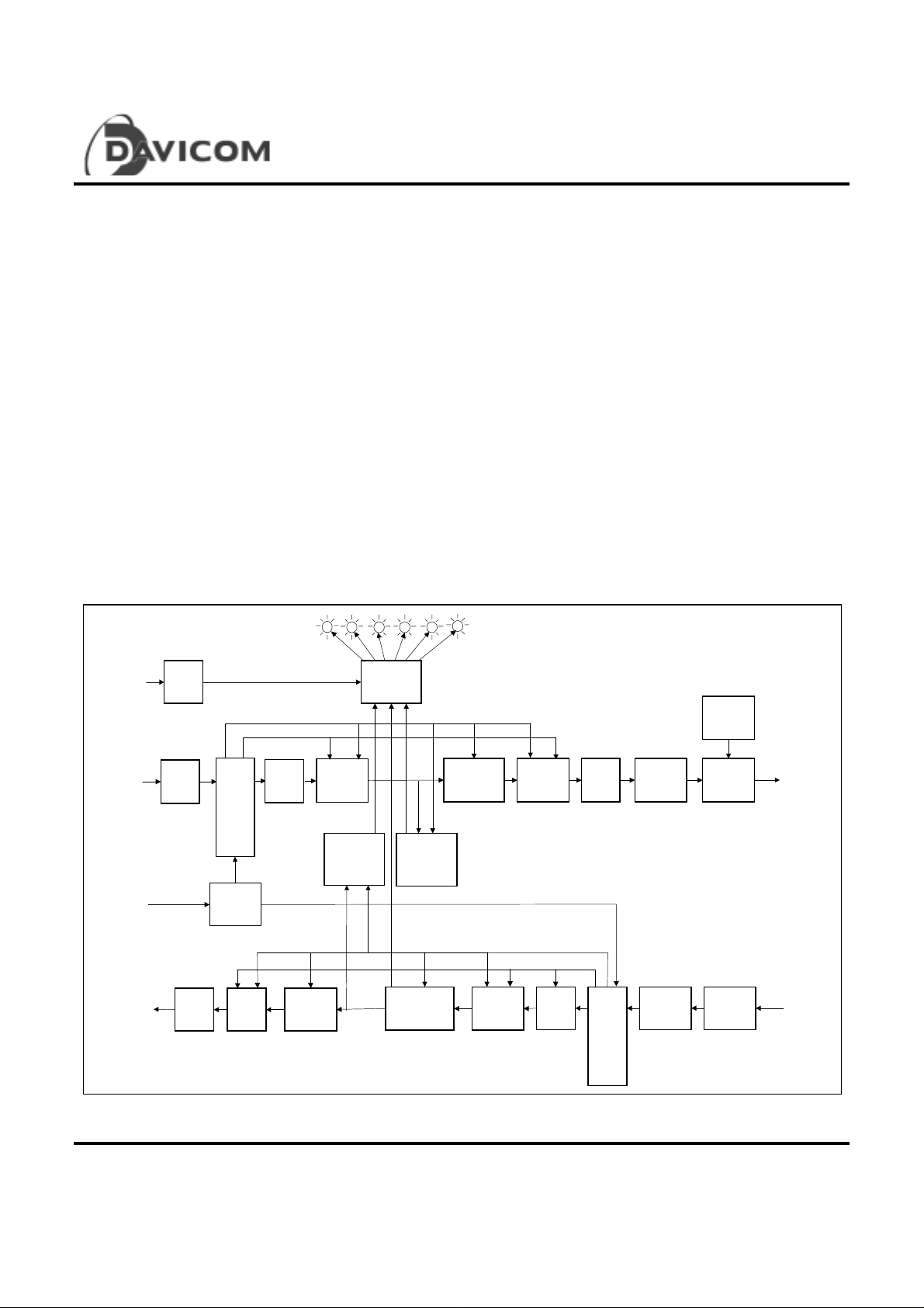
The DM9301 provides two independent clock
Block Diagram
PECLSD
FXSD
RCVR
25M FXRXCLK
125M FXRXCLK
Link Status
Monitor &
LED Driver
recovery circ uits to minimize bit delay through the
converter (no FIFO are used to buffer data between
the FX and TX interfaces). Furthermore, due to the
excellent rise/fall time control by a built-in waveshaping filter, the DM9301 needs no external filter to
transport signals to the media on the 100Base-TX
interface.
Patent-Pending Circ u its
• Smart adaptive receiv er equalizer
• Digital algorithm for high frequency clock/data
recovery circuit
• High speed wave-shaping circuit
Rise/Fall
Time
CTL
NRZI
to
NRZ
NRZ
to
NRZI
RX
CRM
NRZI to
MLT-3
MLT-3 to
NRZI
MLT-3
Driver
Adaptive
EQ
TPTXO+/-
TPRXI+/-
PECLRXI +/-
25M
OSC/XTAL
PECLTXO +/-
PECL
RCVR
PECL
TXMT
RX
CRM
CGM
NRZ
to
NRZI
NRZI
to
NRZ
Parallel
to Serial
Serial to
Parallel
TX Code-
group
Alignment
Monitor
FX Code-
group
Alignment
Monitor
25M TPRXCLK
Descrambler
Scrambler
Serial to
Parallel
Parallel
to Serial
125M TPRXCLK
Final 1
Version: DM9301 - DS -F02
May 8, 2000
Page 2

Table of Contents
DM9301
100Mbps Ethern et Fi ber/Twi sted Pai r Si ngle Chi p Media C onvert er
General Descri pti on................................................1
Block Diagram........................................................1
Table of contents....................................................2
Features.................................................................3
Pin Configuration: DM9301 QFP.............................4
Pin Description.......................................................5
Functional Descr i pti on ..........................................10
100Base-FX to TX Oper ation................................10
T
FX PECL Receiver............................................10
T
FX Receiver Clock Recovery Module ................10
T
FX NRZI to NRZ Converter ...............................10
T
FX Serial to Parallel Converter..........................11
T
FX Code Group Alignment Monitor....................11
T
TX Scrambler....................................................11
T
TX Parallel to Serial Converter ..........................11
T
TX NRZ to NRZI Converter ...............................11
T
TX NRZI to MLT-3 Converter.............................11
T
TX MLT-3 Driver ...............................................11
100Base-TX to FX Operati on................................12
T
TX Signal Detect...............................................12
T
TX Digital Adaptive Equalization........................12
T
TX MLT-3 to NRZI Decoder...............................13
T
TX Clock Recovery Modul e ............................... 13
T
TX NRZI to NRZ Decoder..................................13
T
TX Serial to Parallel Converter..........................13
T
TX Code Group Monitor ....................................13
T
TX Descrambler................................................13
T
FX Parallel to Serial Converter..........................13
T
FX NRZ to NRZI Encoder .................................13
T
Link Monitor and LED Driver .............................13
Abso lu te Maximum Ratings..................................14
DC Electrical Characteristics ................................15
AC Electrical Characteristics.................................16
Timing Wave for ms ...............................................17
T
100BASE-TX to FX Transmit Timing Diagram...17
T
100BASE-FX to TX Transmit Timing Diagram...17
T
5-Bit Symbol 100Base-TX/FX Transm it Timing
Diagram ............................................................17
T
5-Bit Symbol 100Base-TX/FX Receive Timing
Diagram ............................................................18
Applica tion Circ uit (For Reference Only)...............19
Package Information.............................................21
Ordering Informatio n.............................................22
Disclaimer............................................................22
Company Overview..............................................22
Products...............................................................22
Contact Windows..................................................22
Warning...............................................................22
2 Final
Version: DM9301-DS-F02
May 8, 2000
Page 3

Features
DM9301
100Mbps Ethern et Fi ber/Twi sted Pai r Si ngle Chi p Media C onvert er
• 100BASE-TX/FX s ingle-chip media converter
• Total bit delay from FX to TX interface is 20 bit
times (10 bit times each direction).
• Optional propagate HALT on no Link condition
• Compliant with IEEE802.3u 100BASE-TX standard
• Compliant with ANSI X3T12 TP-PMD 1995
standard
• Compliant with ANSI X3.166 FDDI-PMD
• Supports Half and Full Duplex operation 100Mbps,
the DM9301 operates in Full Duplex mode at all
times
• High performance 100Mbps clock generator and
data recovery circuit
• Controlled output edge rates in the 100Base-TX
transmitter without the need for an external filte r
• LED support for FX Link, TX link , FX receive data,
TX receive data, FX code group error and TX code
group error.
• Built in LED test, all LED will light during a reset
condition on the DM9301
• Digital clock recovery and regeneration circuit
usin g a n a d va n ce d dig it al al gorithm to minimi z e
jitter
• Supports diagnostic T X t o TX anal og l oopbac k and
FX to FX analog loopback (Loopback at the NRZI
interface)
• Supports diagnostic T X t o TX di gital loopback and
FX to FX digital loopback (Loopback at the 5B
symbol interface)
• Low-power, high-performance CMOS process
• Available in a 100 QFP package
Final 3
Version: DM9301 - DS -F02
May 8, 2000
Page 4
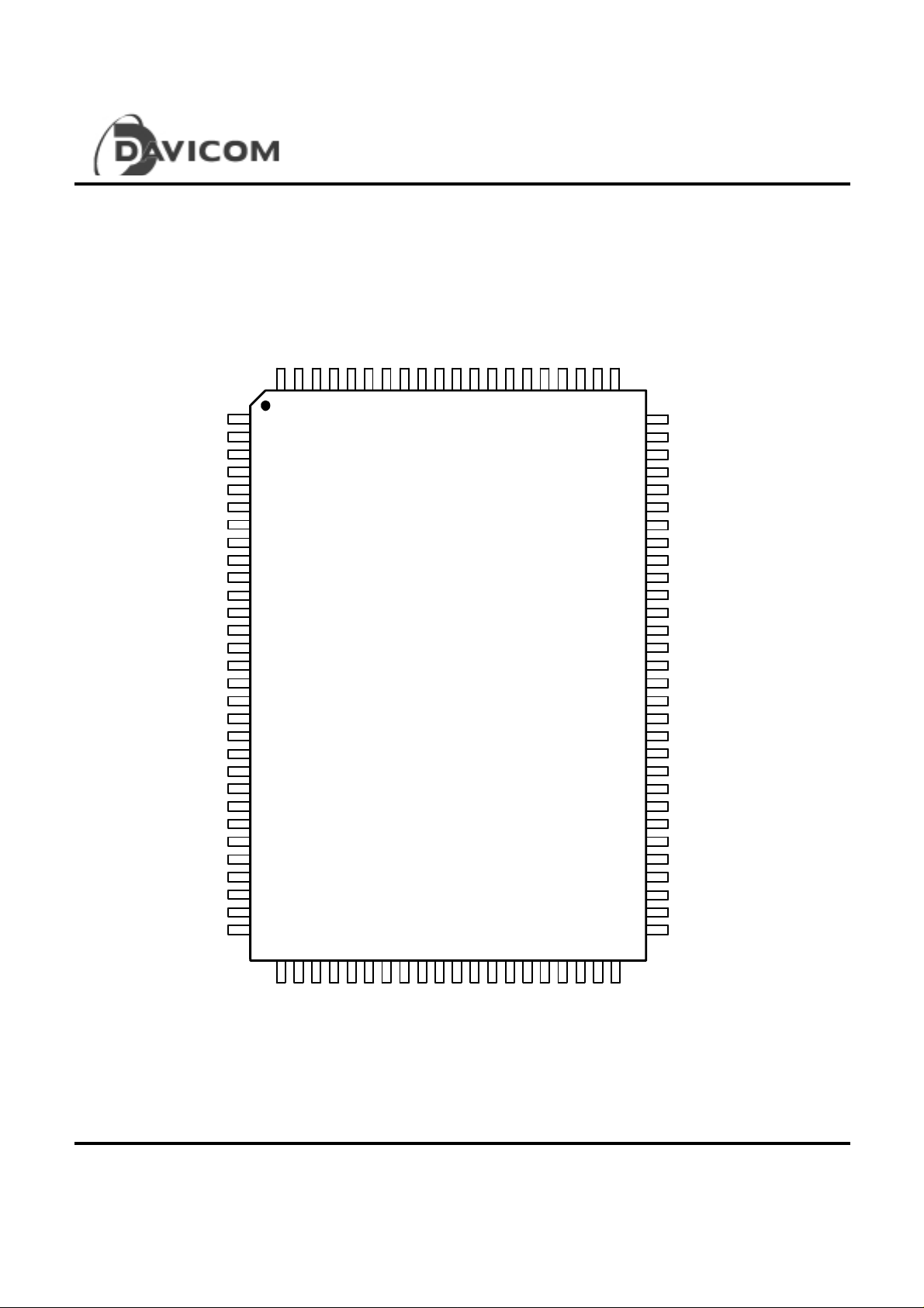
Pin Configu ration: DM9301 F QFP
DM9301
100Mbps Ethern et Fi ber/Twi sted Pai r Si ngle Chi p Media C onvert er
TPRXI+
TPRXI-
AVCC
AVCC
AGND
AGND
AVCC
BGREF
BGRET
AVCC
AGND
AGND
TPTXO-
TPTXO+
AVCC
AGND
AGND
PECLTXO-
PECLTXO+
AGND
AVCC
PECLSD-
PECLSD+
PECLRXI-
PECLRXI+
AVCC
OSC/X1
X2
AGND
OSC/XTL#
1
2
3
4
5
6
7
8
9
10
11
12
13
14
15
16
17
18
19
20
21
22
23
24
25
26
27
28
29
30
AGND
AGND
99
100
32
31
DGND
TXDLPBK
97
98
34
33
TPI2
TPI3
DVCC
FXDLPBK
96
CONFIGA
CONFIGB
93
94
95
92
91
DM9301F
39
38
37
36
35
TPI1
DGND
89
90
424041
TPI0
88
43
TPMUX
DVCC
86
87
45
44
RESET#
TRIDRV
84
85
47
46
DGND
DVCC
TESTMODE
81
82
83
80
79
78
77
76
75
74
73
72
71
70
69
68
67
66
65
64
63
62
61
60
59
58
57
56
55
54
53
52
51
50
49
48
FXERRLED#
RXD0
DGND
RXD1
RXD2
DVCC
RXD3
RXD4
DGND
TXCLK
RXCLK
FXRCVLED#
DGND
FXLNKLED#
DVCC
TPO6
TXLNKLED#
DGND
TXRCVLED#
TPO0
TPO1
DGND
TPO2
TPO3
DVCC
TPO4
TPO5
DGND
TXERRLED#
DVCC
TXD1
AVCC
AGND
DGND
HLTNOLNK
DVCC
TXALPBK
FXALPBK
TPEN
MUXCTL1
DGND
MUXCTL0
BPSCRAM
TXD4
TXD3
TXD2
DVCC
TXD0
FRCFXSD
DGND
4 Final
Version: DM9301-DS-F02
May 8, 2000
Page 5

100Mbps Ethern et Fi ber/Twi sted Pai r Si ngle Chi p Media C onvert er
Pin Description
Pin No. Pin Name I/O Description
Media Interface
1, 2 TPRXI+,
TPRXI-
13, 14 TPTXO-,
TPTXO+
24, 25 PECLRXI-,
PECLRXI+
18, 19 PECLTXO- ,
PECLTXO+
22, 23 PECLSD-,
PECLSD+
Clock and Misc. Interface
27 OSCI/X1 I
28 X2 O
30 OSC/XTL# I
8BGREFI
9BGRETI
I
O
I
O
I
100Mbps-TX Differential Input Pair:
These pins are differential receive input for 100BASETX. They are capable of receiving 100BASE-TX MLT-3
data.
100BASE-TX Differential Output Pa i r:
These outputs drive MLT-3 encoded data over 100Mbps
twisted pair cable and provide controlled rise and fall
times designed to filter the transmitter output,
reducing any associated EMI.
100BASE-FX PECL Receive Data Differential Pair:
These pins are differential receive input for 100BASEFX PECL. They are capable of receiving PECL
100BASE-FX NRZI data.
100BASE-FX Transmit Differential Out pu t Pair:
These outputs drive NRZI encoded data for PECL FX
interface.
100BASE-FX PECL Signal detect:
These pins are differential signals t hat indicate to the
DM9301 that the Optical Module interface is detecting
valid optical energy.
Cryst al or Oscillat or Input:
This pin should connect t o one side of a 25MHz, 50ppm
crystal if OSC/XTL#=0. This pi n is the 25MHz, 50ppm
external TTL oscillator input, if OSC/XTLB=1.
Crystal Oscillat or Output:
The othe r side of a 25MH z, 50ppm c rystal should
connect to thi s pin if OSC/XTL#=0. Leave this pin open
if OSC/XTL#=1.
Cryst al or Oscillat or Selec t or Pin:
OSC/XTL#=0: An external 25MHz, 50ppm crystal
should connect to X1 and X2 pins.
OSC/XTL#=1: An external 25MHz, 50ppm oscillator
should connect to X1 and left X2 pin
open.
Bandga p Voltage R eference Resistor:
It connects to a 6.49KΩ, 1% error tolerance resistor
between this pin and BGRET pin 9 to provide an
accurate current reference for the chip.
Bandgap Return
Return pin for 6.49KΩ resistor connection, DO NOT
CONNECT TO GROUND.
DM9301
Final 5
Version: DM9301 - DS -F02
May 8, 2000
Page 6

100Mbps Ethern et Fi ber/Twi sted Pai r Si ngle Chi p Media C onvert er
Clock and Misc. Interface (Continued)
84 TRIDRV I
85 RESET# I
34 HLTNOLNK I
93 CONFIGA I
95 CONFIGB I
LED Interface
67 FXLNKLED# OD
64 TXLNKLED# OD
69 FXRCVLED# OD
62 TXRCVLED# OD
80 FXERRLED# OD
DM9301
Tristate Digital Output Pin s:
When set high, all digital output pins are set to high
impedance.
Reset: Active Low input that initializes the DM9301,
must be asserted low for 30msecs after VCC is stable.
Send Ha lt on no Link Condition:
Causes the DM9301 to Send out a Halt symbol to the
TX interface if no FX link active or send out a Halt
symbol to the FX interface if no TX link active.
Propagates a no-link condition to the Link P artner if 1,
Idle symbol if 0. Active high
Config A: Must be connected to GND
Config B: Must be connected to GND
FX Link LED:
Indicates Good Link stat us for 100Mbps FX operat ion.
Active low (Open Drain Output)
TX Link LED:
Indicates Good Link stat us for 100Mbps TX operat ion.
Active low (Open Drain Output)
FX Receive LED:
Indicates the presence of receive activity for 100Mbps
FX operation. A ctive low (Open Drain Output)
The DM9301 incorporates a "monostable" function on
the FXRCVLED output. This ensures that ev en
minimum size packets generate adequate LED ON to
insure visibility.
TX Receive LED:
Indicates the presence of receive activity for 100Mbps
TX operation. A ctive low (Open Drain Output)
The DM9301 incorporates a "monostable" function on
the TXRCVLED output. This ensures that ev en
minimum size packets generate adequate LED ON to
insure visibility.
FX Error LED:
Indicates an error was detected by the FX Code Group
Alignment Monitor function on the FX receiver. Active
low (Open Drain Output)
The DM9301 incorporates a "monostable" function on
the FXERRLED output. This ensures that ev en
minimum size errors generate adequate LED ON to
insure visibility.
6 Final
Version: DM9301-DS-F02
May 8, 2000
Page 7

LED Interface(Continued)
52 TXERRLED# OD
Diagnostic Port Interface
36 FXALPBK I
35 TXALPBK I
96 FXDLPBK I
97 TXDLPBK I
79, 77,
76, 74,
73
70 RXCLK O
48, 47,
45, 44,
43
71 TXCLK O
RXD0, RXD1,
RXD2, RXD3,
RXD4
TXD0, TXD1,
TXD2, TXD3,
TXD4
DM9301
100Mbps Ethern et Fi ber/Twi sted Pai r Si ngle Chi p Media C onvert er
TX Error LED:
Indicates an error was detected by the TX Code Group
Alignment Monitor function on the TX receiver. Active
low (Open Drain Output)
The DM9301 incorporates a "monostable" function on
the TXERRLED output. This ensures that ev en
minimum size errors generate adequate LED ON to
insure visibility.
FX Interface Analog Loop Back:
Loops the FX NRZI analog transmit data path to the FX
NRZI analog receive path.
Initiated at a H/W reset. Active high.
TX Interface Analog Loop Back:
Loops the TX NRZI analog transmit data path to the TX
NRZI analog receive path.
Initiated at a H/W reset. Active high.
FX Interface Digital Loop Back:
Loops the FX 5-bit symbol digital transmit data path to
the FX 5-bit symbol digital receive path.
Initiat ed at a H/W reset. Active high.
TX Interface Digital Loop Back:
Loops the TX 5-bit symbol digital transmit data path to
the TX 5-bit symbol digital receive path.
Initiated at a H/W reset. Active high.
0
I
Receive Data 4 through 0:
The receive data 5-bit symbol interface. Data is clocked
out on the falling edge of RXCLK.
Receive Clock:
25 Mhz recovered clock, clock source is selected by the
MUXCTL1 and MUXCTL0.
Transmit Data 4 through 0:
The transmit data 5-bit symbol interface. Data is clocked
in on the rising edge of TXCLK.
Transmit Clock:
25 Mhz recovered clock, clock source is selected by the
MUXCTL1 and MUXCTL0.
Final 7
Version: DM9301 - DS -F02
May 8, 2000
Page 8

100Mbps Ethern et Fi ber/Twi sted Pai r Si ngle Chi p Media C onvert er
Diagnostic Port Interface (Continued)
39, 40 MUXCTL1,
MUXCTL0
DM9301
I
Mux. Control 1 and 0:
Used for testing the DM9301 Data Paths. Set to zero for
normal operati on.
Initiated at a H/W reset. Active high.
65, 54,
55, 57,
58, 60,
61
92, 91, 89,
88
TPO6, TPO5,
TPO4, TPO3,
TPO2, TPO1,
TPO0
TPI3, T PI2 , TPI1,
TPI0,
MUXCTL1 MUXCTL0
0 0 Normal, FX to TX and TX to FX
1 0 TX Transmit from TXD[4:0]
TXCLK from TX PLL
TX Receive to RXD[4:0]
RXCLK from TX receive clock
0 1 FX Transmit from TXD[4:0]
TXCLK from FX PLL
FX Receive to RXD[4:0]
RXCLK from FX receive clock
1 1 TX Transmit from TXD[4:0]
TXCLK from TX PLL
FX Receive to RXD[4:0]
RXCLK from FX receive clock
O
I
Test Port Output:
Reflects the DM9301 internal status. Selection of status
indicators is made by using TPEN and TPMUX.
Initiated at a H/W reset. Active high.
Test Port Input:
Controls the DM9301 internal test features. Selection of
input control is made by using TPEN and TPMUX.
TPEN must be true (one) for t his signal to take effect.
Initiated at a H/W reset. Active high.
DATA PATH
8 Final
Version: DM9301-DS-F02
May 8, 2000
Page 9

100Mbps Ethern et Fi ber/Twi sted Pai r Si ngle Chi p Media C onvert er
Diagnostic Port Interface (Continued)
49 FRCFXSD I
38 TPEN I
87 TPMUX I
41 BPSCRAM I
DM9301
Force FX Signal Detect
Forces the DM9301 FX interface Signal Detect true
Initiated at a H/W reset. Active high.
Test Port Enable:
Enables the DM9301 Test Port features.
Initiated at a H/W reset. Active high.
Test Port Mux:
Controls the DM9301 Test Port Input and Output bits.
A value of zero indicates the TX interface and a value of
one indicates the FX interface. TPEN must be true (one)
for this signal to take effect.
Initiated at a H/W reset. Active high.
Bypass Scrambler:
Controls the DM9301 TX interface Scrambler/Descrambler function. A value of zero indicates to
scramble and de-scramble the TX interface 5-bit
symbol data to and from the FX interface. A value of one
bypasses the scrambl er/de- scrambler function.
Initiated at a H/W reset. Active high.
Power a nd Ground P i ns :
The power (VCC) and ground (GND) pins of the DM9301 are grouped in pairs of two categories - Digital
Circuitry Power/Ground Pairs and Analog Circuitry Power/Ground Pair.
Group A - Digital Supply Pairs
33, 42, 50, 53,
63, 68, 82, 90,
98
37, 46, 51, 66,
81, 94
Group B - Analog Circuit Supply Pairs
5, 6, 11, 12, 20,
29, 32, 99, 100,
3, 4, 7, 15, 21,
26, 31
DGND P Digital Logic Ground.
DVCC P Digital Logic power supply
AGND P Analog circuit ground
AVCC P Analog circuit power supply
Final 9
Version: DM9301 - DS -F02
May 8, 2000
Page 10

100Mbps Ethern et Fi ber/Twi sted Pai r Si ngle Chi p Media C onvert er
Functional Description
The DM9301 Fast Ethernet single-chip TX/FX media
converter, provides the functionality as specified in
IEEE802.3, integra tes the co mplete 100BASE -TX and a
PECL op ti c mod ule in te rfac e for 100Base-FX. The
DM9301 implements the PCS, PMA, and TP-PMD
sublayer functions, as defined by specification. The term
“X” will be used to describe the sections used in the fiber
PHY layer interface. The term “X” will be used to describe
the sections used in the twisted-pair PMD layer interface.
100BASE-FX to TX Operation
The block diagram in figure 1 provides an overview of the
functional blocks contained in the FX to TX media
conver ter in ter face .
DM9301
FX PECL Receiver
The PECL receiver receives NRZI encoded, differential
Pseudo Emitter Coupled Logic level signal. The receiver
converts the receive signal into a single-ended NRZI
signal and presents this signal to the FX Clock Recovery
Module.
FX Receiver Clock Recovery Module
The FX Clock Recovery Module accepts NRZI data from
the PECL receiver. The FX Clock Recovery Module locks
onto the data stream, using a Phase Lock Loop (PLL) an d
extracts the 125Mhz reference clock. The extracted and
synchronized clock and data are presented to the FX
NRZI to NRZ Decoder.
The FX to TX interface includes the following functional
blocks:
• FX PECL Receiver
• FX Receiver Clock Recovery Module
• FX NRZI to NRZ Converter
• FX Serial to Par a lle l Con ver ter
• FX Code Group Alignment Monitor
• TX Scrambler
• TX Paralle l to Ser ia l Con ver ter
• TX NRZ to N R ZI C on ver ter
• TX NRZI to MLT-3 Converter
• TX MLT-3 Driver
PECLSD
PECLRXI +/-
25M
OSC/XTAL
FXSD
RCVR
FX
PECL
RCVR
FX
RX
CRM
CGM
25M FXRXCLK
125M FXRXCLK
FX
NRZI
to
NRZ
FX Serial
Parallel
FX Link
Status
Monitor
to
FX Code-
group
Alignment
Monitor
FX NRZI to NRZ Converter
The receive data stream is required to be NRZI encoded
for compatibility with the standards for 100Base- FX. This
conversion process must be reversed on the transmit end.
The FX NRZI to NRZ decoder, r ec eives the NRZI
data stream from the FX Clock Recovery Module
and converts it to a NRZ data stream to be
presented to the FX Serial to Parallel conversion
block.
Rise/Fall
Time
CTL
TX
Scrambler
TX
Parallel
to Serial
TX
NRZ
to
NRZI
TX
NRZI to
MLT-3
MLT-3
Driver
TPTXO+/-
FX to TX B loc k D iagr am
Figure 1
10 Final
Version: DM9301-DS-F02
May 8, 2000
Page 11

DM9301
100Mbps Ethern et Fi ber/Twi sted Pai r Si ngle Chi p Media C onvert er
FX Seria l to Par allel C onve rter
The Serial to Parallel converter receives a serial
data stream from the NRZI to NRZ converter, and
converts the data stream to parallel data to be
presented to the scrambler. The parallel data format
presented to the TX scrambler is 5B coded.
FX Code Group Alignment Monitor
The FX Code Group Alignment block receives nonaligned 5B data from the FX Serial to Parallel
converter and monitors it for 5B code group
violations. F X Code Group Alignment oc c ur s after
the J/K is detected, and subsequent data i s
monitored on a fixed boundary. If a v iolation is
detected, t he FX Code Group Alignment M onitor
block signal s the error t o the Link Status Monit or
block. In turn, the Link Status Monitor block flashes
the FX error LED (FXERRLED#).
TX Scrambler
The scrambler also receives data from the FX Serial
to Parallel converter. Data from the serial to parallel
conversion block is 5B symbol encoded. The
scrambler i s required to control the radiated
emissions (EMI) by spreadi ng the transmit energy
across the frequency spectrum at the media
connector and on the twisted pair cable in 100BaseTX transmit oper ation.
By scra mbling the data, the total energy presented
to the cable is randomly distributed over a wide
frequency range. Without the scrambler, energy
levels on the cable could peak beyond FCC
limitations at frequencies related to repeated 5B
sequences like conti nuous tr ansmission of IDLE
symbols. The scrambler output is combined with the
NRZ 5B data from the FX Serial to Parallel
converter via an XOR logic function. The result is a
scrambled data stream with sufficient randomization
to decrease radiated emissions at critical
frequencies.
TX Parallel to Serial Converter
The TX Parallel to Serial conver ter receives parallel
5B scrambled data from the scr ambler and
serializ es it ( c onverts it from a parallel to a serial
data stream). The serialized data stream is then
presented to the NRZ to NRZI converter block
TX NRZ to NRZI Converter
After the tr ansmit data stream has been scram bled
and serialized, the data must be NRZI encoded for
compatibility with the TP-PMD standard for
100Base-TX transm ission over Category-5
unshielded twisted pair cable.
TX MLT-3 Converter
The MLT-3 conversion is accomplished by
converting the data stream output from the NRZI
encoder into two binary data streams with
alternately phased logic one events.
TX MLT-3 Driver
The two binary data streams created at th e MLT-3
converter are fed to the twisted pair output driver
which converts these streams to current sources
and alternately drives either side of the transmit
transformer primary winding resulting in a minimal
current MLT-3 signal .
Final 11
Version: DM9301 - DS -F02
May 8, 2000
Page 12

DM9301
100Mbps Ethern et Fi ber/Twi sted Pai r Si ngle Chi p Media C onvert er
100Base-TX to FX Operation
The block diagram in figure 2 provides an overview of the
functional blocks contained in the TX to FX media
conver ter in ter face .
The TX to FX interface contains the following functional
blocks:
• TX Digital Adaptive Equalization
• TX MLT-3 to NR ZI
• TX Clock Recovery Module
• TX NRZI to NRZ Decoder
• TX Serial to Parallel Conversion
• TX Descrambler
• TX Code Group Alignment Monitor
• FX Paralle l to Ser ia l Con vers ion
• FX NRZ to NRZI
• FX PECL Transmitter
TX Signal Detect
The signal detect function meets the specifications
mandated by the ANSI XT12 TP-PMD100Base-TX
standards for both voltage thresholds and timing
parameters.
TX Di gita l Ada ptiv e Eq ual izat ion
When transmitting data at high speeds over copper
twisted pair cable, attenuation based on frequency
becomes a concern. In high speed twisted pair signaling,
the frequency content of the tran smitt e d signal can vary
greatly during normal operation based on the randomness
of th e s cr a mbled da t a stream. This varia tion i n si gnal
attenuation caused by frequency variations must be
compensated for to ensure the integrity of the received
data. In order to ensure quality transmission when
employing MLT-3 encoding, the compensation must be
able to adapt to various cable lengths and cable types
depending on the installed environment. The selection of
long cable lengths for a given implementation, requires
significant compensation which will be over-kill in a
situation that includes shorter, less attenuating cable
lengths. Conversely, the selection of short or intermediate
cable lengths requiring less compensation will cause
serious under-compensation for longer length cables.
TX Link
Status
Monitor
TX Code-
group
Alignment
Monitor
25M
OSC/XTAL
PECLTXO +/-
TX
PECL
TXMT
CGM
TX
NRZ
to
NRZI
FX
Parallel
to Serial
25M TPRXCLK
TX
Descrambler
TX
Serial to
Parallel
125M TPRXCLK
TX
NRZI
to
NRZ
TX
CRM
TX
MLT-3 to
NRZI
TX
Adaptive
EQ
TPRXI+/-
TX to FX Block Diagram
Figure 2
12 Final
Version: DM9301-DS-F02
May 8, 2000
Page 13

DM9301
100Mbps Ethern et Fi ber/Twi sted Pai r Si ngle Chi p Media C onvert er
Therefore, the compensation or equali zat ion m u st be
adaptive to ensure proper co nditi oni n g of the re cei v ed
signal independent of the cable length.
TX MLT-3 to N RZI D eco der
The DM9301 decodes the MLT-3 information from the TX
Digital Adaptive Equalizer into NRZI data.
TX Clock Recovery Module
The TX Clock Recovery Module accepts NRZI data
from the MLT-3 to NRZI decoder. The TX Clock
Recovery Module locks onto the data stream and
extracts the 125M hz referenc e clock . The extract ed
and synchronized clock and data are presented to
the NRZI to NRZ Decoder.
TX NRZI to NRZ Decoder
The TX transmit data stream is requir ed to be NRZI
encoded in for compatibility with the TP-PMD
standard for 100Base-TX transmission over
Category-5 unshielded twisted pair ca ble. This
conversion process must be reversed on the
receive end. The NRZI to NRZ decoder, receives
the NRZI data stream from the TX Clock Recovery
Module and converts it to a NRZ data stream to be
presented to the TX Serial to Parallel conversion
block.
TX Serial to Parallel Co nv er te r
The TX Serial to Parallel conv er ter receives a serial
data stream from the TX NRZI to NRZ decoder, and
converts the data stream to parallel data to be
presented to the TX descrambler. The parallel data
format presented to the TX descrambler is 5B
coded.
TX Code Group Monitor
The TX Code Group Alignment block receives nonaligned 5B data from the TX descrambler and
monitors it for 5B code group violati ons. TX Code
Group Alignment occurs after the J/K i s detec ted,
and subsequent data is monitored on a fixed
boundary. If a violation is detected, the TX Code
Group Monitor block signals the error to the Link
Status Monitor block. In turn, the Link Status
Monitor bloc k flashes the TX error LED
(TXERRLED#).
TX Descrambler
Because of the scrambling process required to
control the radiated emissions of transmit data
streams, the receiver must descramble the receive
data streams. The TX Descrambler receives
scr ambled parallel dat a streams fr om the Serial to
Parallel converter, descrambles the data streams,
and presents the data streams to the Code Group
alignment block.
FX Parallel to Serial Converter
The FX Parallel to Serial Converter receives parallel
5B data from the TX de-scrambler and serializes it
(converts it f r om a parallel to a seria l d ata stream).
The serialized data stream is then presented to the
FX NRZ to NRZI Encoder block
FX NRZ to NRZI Encoder
After the tr ansmit data stream has been serialized,
the data must be NRZI encoded for compatibility
with the standard for 100Base-FX.
Link Monitor and LED Driver
The Link Monitor block monitors both the TX and
FX interfaces for link active, receive data and erring
5-bit stream.
The Link Monitor has the ability to detect each
interfac es li nk status. The TX will transmit either an
Idle symbol or a Halt symbol if the FX link is not
established. Conversely the FX will transmit either
an Idle symbol or a Halt symbol if the TX link is not
established. When an o Link” con diti o n exists, the
interfac e pin call ed LTNOLNK” will cause Halt
symbols to be transmitted instead of Idle symbols.
The link active LED is a static indic ation of th e TX
and FX links. It will be true to indicate the presence
of a link. The receive data and error LED are
generated through a ne-Shot” so that even the
smallest receive or error condition will be indicated.
Final 13
Version: DM9301 - DS -F02
May 8, 2000
Page 14

100Mbps Ethern et Fi ber/Twi sted Pai r Si ngle Chi p Media C onvert er
Absolute Maxim um Ratin gs*
Absolute Maximum Ratings ( 25°°°°C )
Symbol Parameter Min. Max. Unit Conditions
CC
V
IN
V
OUT
V
Tstg Storage Temperature Rang (Tstg) -65 +150
PD Power Dissipation (PD) --- 1 W
LT Lead Temp. (TL, Soldering, 10 sec.) -- - 240
ESD ESD rating (Rzap=1.5K,Czap=100pF) --- 4000 V
Operat ing C o nd itio ns
Symbol Parameter Min. Max. Unit Conditions
DVCC,AV
CC
Tc Case Temperature 0 85
PD
(Power Dissipation)
Max. Supply Voltage -- 7.0 V Non-operating
DC Input Voltage (VIN)-0.55.5V
DC Output Voltage(V
OUT
)-0.55.5V
°C
°C
Supply Voltage 4.75 --- 5.25
°C
100BASE-TX --- 200 mA 5V
DM9301
*Comments
Stresses above those listed under “Absolute
Maximum Ratings” may cause permanent damage to
the device. These are stress ratings only. Functional
operation of this device at these or any other
conditions above those indicated in the operational
sections of this specification is not im plied. Exposure
to absolute maximum rating conditions for extended
periods may aff ect dev ic e reliability.
14 Final
Version: DM9301-DS-F02
May 8, 2000
Page 15

DM9301
100Mbps Ethern et Fi ber/Twi sted Pai r Si ngle Chi p Media C onvert er
DC Electrical Characteristics
(VCC = 5V)
Symbol Parameter Min. Typ. Max. Unit Conditions
TTL In puts
(DPLXSEL, RESET# )
IL
V
IH
V
IL
I
IH
I
Input Low Voltage 0.8 V IIL = -400uA
Input High Voltage 2.0 V IIH = 100uA
Input Low Current -200 uA VIN = 0.4V
Input High Current 100 uA VIN = 2.7V
LED Driv er Outputs
(FXLINKLED#, T XLINK LE D#, FXRXD#,RXRXD#)
OL
V
OH
V
Output Low Voltage 0.4 V IOL = 8mA
Output High Voltage 2.4 V IOH = -0.1mA
TPTX Receiver
ICM
V
RXI+/RXI- Input Common-Mode
Voltage
1.5 2.0 2.5 V
100 Ω Termination
Across
TPTX Transmitter
ITD100 100TXO+/- 100BASE-TX Mode
Differential Output Current
ǔ
mA
PECL FX Transmitter
IFD100 PECLTX+/- 100BASE-FX Mode
Differential Output Current
mA
OH
V
OL
V
PECL Output Voltage – High VCC-
1.05
PECL Output Voltage – Low VCC-
1.81
VCC-
0.88
VCC-
1.62
V
V
Final 15
Version: DM9301 - DS -F02
May 8, 2000
Page 16

DM9301
100Mbps Ethern et Fi ber/Twi sted Pai r Si ngle Chi p Media C onvert er
AC Electrical Characteristics
(Over full range of operating condition un l e s s specified otherw is e)
Symbol Parameter Min. Typ. Max. Unit Conditions
Transmitter
TR/F
t
TM
t
100TXO+/- Differential Rise/Fall Time 3.0 5.0 ns
100TXO+/- Differential Rise/Fall Time
-0.5 0.5 ns
Mismatch
TDC
t
100TXO+/- Differential Output Duty Cycle
-0.5 0.5 ns
Distortion
T/T
t
100TXO+/- Differential Output Peak-to-
300 ps
Peak Jitter
OST
X
100TXO+/- Differential Voltage Overshoot 5 %
PECL Transmitter (FX Transmit Interface)
TR/F
pt
pt
TM
100FXTD+/- Differential Rise/Fall Time 1.0 2.0 ns
100FXTD+/- Differential Rise/Fall Time
-0.5 0.5 ns
Mismatch
TDC
pt
100FXTD+/- Differ ential Output Duty Cycle
-0.5 0.5 ns
Distortion
PPJ
pt
100FXTD+/- Differential Output Peak-to-
300 ps
Peak Jitter
DDJ
pt
100FXTD+/- Differential Output Data
2.0 ns
Dependent Jitter
Clock Specifications
NTOL
X
TX Input Clock Fr equenc y T oler anc e
-50 +50 ppm 25MHz Frequency
(Oscillator or Crystal input frequency)
BTOL
X
PWH
t
PWL
t
RPWH
t
RPWL
t
TX Output Clock Frequency T oler anc e -100 +100 ppm 25MHz Frequency
OSC Pulse Width High 14 ns
OSC Pulse Width Low 14 ns
RX_CLK Pulse Width High 14 ns
RX_CLK Pulse Width Low 14 ns
16 Prel im ina ry
Version: DM9301-DS-F02
May 8, 2000
Page 17

100Mbps Ethern et Fi ber/Twi sted Pai r Si ngle Chi p Media C onvert er
Timing Waveforms
100BASE-TX to FX Transmit Timing Diagram
TPRXI+/-
t
FX
pd
PECLTX+/-
100BASE-TX to FX Transmit Timing Parameters
DM9301
Symbol Parameter Min.
FX
t
TPRXI+/- to PECLTX+/- Out (FX Latency) - - 10 BT
pd
100BASE-FX to TX Transmit Timing Diagram
PECLTX+/-
t
TX
pd
TPRXI+/-
100BASE-FX to TX Transmit Timing Parameters
Symbol Parameter Min.
TX
t
PECLRX+/- to TPTXo+/- Out (TX
pd
Latency)
5-Bit Symbol 100Base-TX/FX Transmit Timing Diagram
TXCLK
t
TXD [4:0]
TX
S
t
TX
h
Typ1.
Typ1.
Max. Unit Conditions
Max. Unit Conditions
--10BT
t
TX
t
100TX+/100FX+/-
Final 17
Version: DM9301 - DS -F02
May 8, 2000
TXD
pdtpo
t
TXD
pdfxo
rft
Page 18

100Mbps Ethern et Fi ber/Twi sted Pai r Si ngle Chi p Media C onvert er
5-Bit Symbol 100Base-TX/FX Transmit Timing Parameters
DM9301
Symbol Parameter Min.
TX
t
TX
t
TXD[4:0] Setup To TX_CLK High 11 - - ns
s
TXD[4:0] Hold From TX_CLK
h
0--ns
1 Max. Unit Conditions
Typ.
High
TXD
t
pdtpo
TXD[4:0] Sampled To TPTXO
--6BT
(TXD to TP Latency)
TXD
t
pdfxo
TXD[4:0] Sampled To PECLTXO
--4BT
(TXD to FX Latency)
TX
t
100TX Driver Rise/Fall Time 3 4 5 ns 90% To 10%, Into
r/f
100ohm Differ enti al
1
. Typical values are at 25and are for design aid only; not guaranteed and not subject to production testing.
5-Bit Symbol 100Base-TX/FX Receive Timing Diagram
RXCLK
RXD [4:0]
TX RXI+/FX RXI+/-
t
RX
t
RX
S
h
t
RXD
pdtxi
t
RXD
pdfxi
5-Bit Symbol 100Base-TX/FX Receive Timing Parameter
Symbol Parameter Min.
RX
t
RXD[4:0) Setup To RX_CLK
s
10 - - ns
Typ1.
Max. Unit Conditions
High
RX
t
RXD[4:0]Hold From RX_CLK
h
10 - - ns
High
RXD
t
TXRXI In To RXD[0:3] Out (Rx
pdtxi
--6BT
Latency)
RXD
t
PECLRDI In To RXD[4:0] Out
pdfxi
--4BT
(Rx Latency)
18 Prel im ina ry
Version: DM9301-DS-F02
May 8, 2000
Page 19

DM9301
100Mbps Ethern et Fi ber/Twi sted Pai r Si ngle Chi p Media C onvert er
MII Application Circuit: DM9301 QFP
Fiber LEDs
.125
J1
Power
Jack
SOT-223 3.3v REG
.80
.120
.080 holes with Plating
.018 holes
(For Reference Only)
DM9301 Sample, suggested placement
Twisted LEDs
100 PIN QFP U1
PIN 1
PE68551 LAN Xformer
PIN 1
PIN 1
J2
RJ45
Footprints for either
Optical module
0.25 in
.120 Holes
0.80 in c h
CUT AWAY POWER PLANE IN
THIS AREA (See Sc h ema tic )
THIS IS A ISOLATION BARRIER
.350
Final 19
Version: DM9301 - DS -F02
May 8, 2000
Page 20

DM9301
100Mbps Ethern et Fi ber/Twi sted Pai r Si ngle Chi p Media C onvert er
MII Application Circuit: DM9301 QFP
(Continued, For Ref er enc e Only )
20 Prel im ina ry
Version: DM9301-DS-F02
May 8, 2000
Page 21

DM9301
100Mbps Ethern et Fi ber/Twi sted Pai r Si ngle Chi p Media C onvert er
Package In form ation
QFP 100 L Ou tl ine D ime nsi ons Unit: Inches/mm
D
H
D
81100
1
F
30
Seating Plane
31
e
G
See Detail F
80
E
E
H
51
50
b
D
2
A
A
1
A
y
D
E
G
c
Symbol Dimensions In Inches Dimensions In mm
A 0.130 Max. 3.30 Max.
1
A
2
A
0.004 Min. 0.10 Min.
0.1120.005 2.850.13
b 0.012 +0.004 0.31 +0.10
-0.002 -0.05
c 0.006 +0.004 0.15 +0.10
-0.002 -0.05
D 0.5510.005 14.00+/-0.13
E 0.7870.005 20.00+/-0.13
e
0.026 0.006 0.650.15
F 0.742 NOM. 18.85 NOM.
D
G
E
G
D
H
E
H
0.693 NOM. 17.60 NOM.
0.929 NOM. 23.60 NOM.
0.7400.012 18.800.31
0.9760.012 24.790.31
L 0.0470.008 1.190.20
L
1
0.0950.008 2.410.20
y 0.006 Max. 0.15 Max.
θ 0° ~ 12° 0° ~ 12°
G
D
~
~~
L
1
L
Detail F
Note:
1. Dimension D & E do not include resin fins.
2. Dimension GD & GE are for PC Board surface mount pad pitch design reference only.
3. All dimensions are based on metric system.
Final 21
Version: DM9301 - DS -F02
May 8, 2000
Page 22

DM9301
100Mbps Ethern et Fi ber/Twi sted Pai r Si ngle Chi p Media C onvert er
Ordering Information
Part Number Pin Count Package
DM9301F 100 QFP
Disclaimer
The information appearing in this publication i s b e li ev e d to
be accurate. Integrated circuits sold by DAVICOM
Semiconductor are covered by the warranty and patent
inde mn ific a tio n pr ovisio n s stip ulated in the te rms of sale
only. DAVICOM makes no warranty, express, statutory,
implied or by description regarding the i nformation in this
publication or regarding the information in this publication or
regarding the freedom of the described chip(s) from patent
infringement. FURTHER, DAVICOM MAKES NO
WARRANTY O F MERCH ANTABIL ITY OR FITNESS FOR
ANY PURPOSE. DAVICOM reserves the right to halt
production or alter the specifications and prices at any time
without notice. Accordingly, the reader is cautioned to verify
that th e da t a sheets and othe r information in this publication
are current before p lacing orders. Products described
herein are intended for use in normal commercial
applications. Applications involving unusual environmental
or r elia b ility re q uir eme nts, e.g. m ilitar y equi pme nt o r me dic al
life support equipment, are specifically not recommended
without additional processing by DAVICOM fo r such
applications. Please note that ap plication circuits illustrated
in this document are for reference pur poses only.
DAVICOM ‘s terms and conditions printed on the order
acknowledgment govern all s ales by DAVICOM. DAVICOM
will not be bound by any terms inconsistent with these
unless DAVICOM agrees otherwise in writing. Acceptance
of the buyer’s orders shall be based on these terms.
Company Ov erview
DAVICOM Semiconductor, Inc. develops and manufactures
integrated circuits for integration into data communication
products. Our mission is to design and produce IC produc ts
that are the industry’s best value for Data, Audio, Video, and
Internet/Intranet applications. To a chieve this goal, w e h ave
built an organization that is able to develop chipsets in
response to the evolving technology requirements of our
custo mers w hile s ti ll de liver ing p rod u cts that meet th eir co st
requirements.
Products
We offer only products that satisfy high performance
requirements and which are compatible with major
hardware and software standards. Our curren tly av ailable
and soon to be released products ar e based on our
proprietary designs and deliver high quality, high
performance chipsets that comply with modem
communication standards and Ethernet networking
standards.
Contact Windows
For additional information about DAVICOM products, contact the sales department at:
Headquarters
Hsin-c hu Off ice:
3F, No. 7-2, Industry E. Rd., IX,
Science-based Park,
Hsin-c hu C ity , Ta iw an , R. O.C .
TEL: 886-3-5798797
FAX: 886-3-5798858
WARNING
Conditions beyond those listed for the absolute maximum may destroy or damage the products. In addition, conditions for sustained periods at near the
limits of the operating ranges will stress and may temporarily (and permanently) affect and damage structure, performance and/or functio n.
22 Prel im ina ry
Taipei Sales & Marketing Office:
8F, No. 3, Lane 235, Bao-chiao Rd.,
Hsin -t ien C ity , Ta ip ei, Ta iwa n, R. O.C .
TEL: 02-29153030
FAX: 02-29157575
Email: sales@davicom.com.tw
Davicom USA
Sunnyvale, California
1135 Kern Ave., Sunnyvale,
CA94086, U.S.A.
TEL: 1-408-7368600
FAX: 1-408-7368688
Email: sales@davicom8.com
Version: DM9301-DS-F02
May 8, 2000
 Loading...