

Page 1
General Descri ption
DM9102A
Single Chi p Fast E thern et NIC c ont roller
The DM9102A is a fully integrated and cost-effective single
chip Fast Ethernet NIC controller. It is designed with the low
power and high performance process. It is a 3.3V device
with 5V tolerance then it s upports 3.3 V and 5V signaling.
The DM9102A provides direct interface to the PCI or the
CardBus. It supports bus master capability and fully
complies with PCI 2.2. In media side, The DM9102A
interfaces to the UTP3,4,5 in 10Base-T and UTP5 in
100Base-TX. It is fully compliance with the IEEE 802.3u
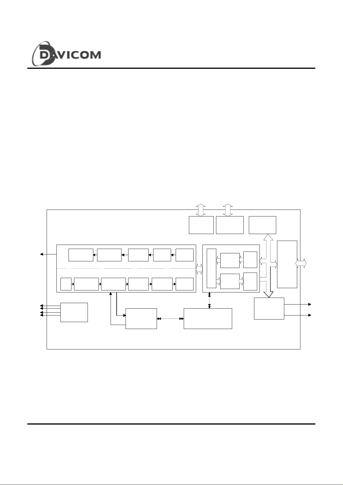
Block Diagr am
PHYceiver
TX+/-
RX+/-
MLT3 to NRZI NRZI to NRZ
AEQ
NRZ to NRZINRZI to MLT3
Parallel to
Serial
Parallel to
Serial
Scrambler
Scrambler
De-
Spec. Its auto-negotiation function will automatically
configure the DM9102A to take the maximum advantage of
its abilities. The DM9102A is also support IEEE 802.3x fullduplex flow control.
The DM9102A supports two types of power-management
mechanisms. The main mechanism is based upon the
OnNow architecture, which is required for PC99. The
alternative mechanism is based upon the remote Wake-OnLAN mechanism.
4B/5B
Encoding
4B/5B
Decoding
EEPROM
Interface
Boot ROM /
MII Interface
MAC
Machine
MII
MachineRXFIFO
TX
RX
TX
FIFO
DMA
PCI
Interface
Power
LED Driver
Autonegotiation
Final 1
Version: DM9102A-DS-F03
August 28, 2000
MII Management Control
& MII Register
Management
Block
PME#
WOL
Page 2

Table of Conten ts
DM9102A
Single Chi p Fast E thern et NIC c ont roller
General Description .............................................................1
Block D iag ra m...................................................................... 1
Feature s...............................................................................4
Pin Configuration: DM9102A 128pin QFP..........................5
Pin Configuration: DM9102A 128pin TQFP .......................6
Pin De sc ript ion.....................................................................7
- PCI Bus and CardBus Interface Signals.........................7
- Boot ROM and EEPROM Interface................................8
T
Multip lex M ode ................................................................8
T
Direct M ode....................................................................10
- LED P ins.........................................................................11
- Netw ork Inter face...........................................................1 2
- Miscellaneous Pins.........................................................12
- Pow er Pin s.....................................................................13
- Note: L E D M ode............................................................13
Regis ter De fin ition..............................................................14
✧ PC I C on figu rat ion R egis ter s..........................................14
Key to De faul t.....................................................................14
T
Identification ID...............................................................15
T
Command & Status........................................................15
T
Revisio n ID.....................................................................17
T
Miscellaneous Function .................................................18
T
I/O Bas e Add res s...........................................................18
T
Memory Mapped Base Address....................................19
T
Subsystem Identification................................................19
T
CardBu s CIS P oi nter......................................................20
T
Expansion ROM Base Address.....................................21
T
Capabilities Pointer.........................................................21
T
Interrupt & Latency Configuration..................................22
T
Device Spe ci fic Configuration Register.........................22
T
Power Management Register........................................23
T
Power Management Control/Status..............................24
✧ C ontr o l and Sta tu s R eg iste r ( CR)..................................25
Key to De faul t.....................................................................25
1. System Cont rol Re gist er (CR0).....................................2 6
2. Trans mi t Des cr ipto r Po ll D ema n d (CR 1)......................2 7
3. Receive Descriptor Poll Demand (CR2).......................27
4. Rece i ve D es cripto r Bas e Ad dre ss (C R3).....................27
5. Trans mi t Des cr ipto r Bas e Add res s (CR 4)....................28
6. Network Status Report Register (CR5).........................28
7. Netw or k Ope rat ion R egis ter (C R6)...............................30
8. Interru p t Mas k Register (C R7)...................................... 32
9. Statistical Counter Register (CR8)................................ 33
10. PROM & Management Access Register (CR9) ........ 34
11. Prog ra mmi ng R OM Add res s Re gis ter ( CR 10).......... 35
12. General Purpose Timer Register (CR11)................... 35
13. PHY S tatu s R eg is ter (CR 12)...................................... 35
14. Sa mple Fra m e A cc es s Reg iste r (CR1 3).................... 36
15. Sa mple Fra m e D a ta Reg is ter (C R14)........................ 36
16. Watching & Jabber Timer Register (CR15)................ 36
✧ CardBus Status Changed Register..............................39
1. Function Event Reg ister : (offs et 80 h)............................ 39
2. Function Event Mask Register: (offset 84h).................. 39
3. Fun ctio n P res en t S tate Re gis ter : (o ffse t 8 8h )............... 39
4. Fun ctio n Fo rce E ven t Re g iste r: (o ffse t 8 Ch)................4 0
✧ PHY Manage ment Register Set...................................41
Key To D efau lt................................................................... 41
Basic Mode Control Register (BMCR)
- Regis ter 0......................................................................... 42
Basic Mode Status Register (BMSR)
- Regis ter 1......................................................................... 43
PHY ID Identifier Register #1 (PHYIDR1)
- Regis ter 2......................................................................... 44
PHY ID Identifier Register #2 (PHYIDR2)
- Regis ter 3......................................................................... 44
Auto-negotiation Advertisement Register (ANAR)
- Regis ter 4......................................................................... 44
Auto-negotiation Link Partner Ability Register (ANLPAR) -
Regis ter 5........................................................................... 45
Auto-negotiation Expansion Register (ANER)
- Regis ter 6......................................................................... 46
DAVICOM Specified Configuration Register (DSCR)
- Regis ter 10....................................................................... 46
DAVIC OM S pec i fied Co n figura tio n a n d Status Regi ste r
(DSCSR ) - R eg iste r 11...................................................... 47
10Base-T Configuration/Status (10BTSCRCSR)
- Regis ter 12....................................................................... 48
Functio na l D es cr ip tio n....................................................... 49
✧ System Buffer Management ......................................... 49
1. Over view........................................................................ 49
2. Data Structure and Descriptor List................................49
3. Buffer Management: Chain Structure Method.............. 49
5. Des crip tor L ist: Bu ffer De s crip tor Fo r mat...................... 49
(a). Re ce i ve Des cr ipto r Fo rma t......................................... 49
2 Final
Version: DM9102A-DS-F03
August 28, 2000
Page 3

DM9102A
Single Chi p Fast E thern et NIC c ont roller
6. Example of DM9102A SROM Format.......................... 63
(b). Tran s mit D es cripto r For mat .........................................51
✧ Initialization Procedure...................................................54
Data Bu ffer Proce ss ing A lgor ith m.....................................54
1. Rece i ve D ata Bu ffer Pro ces s ing...................................54
2. Trans mi t Da ta Bu ffer Pr oce ss ing..................................55
✧ N etw or k Fun c tion...........................................................56
1. Over view.........................................................................56
2. Receive Process and State Machine............................56
a. Reception Initiation ....................................................... 56
b. Address Recognition....................................................5 6
c. Frame Decapsulation...................................................56
3. Transmit Process and State Machine...........................56
a. Transmit Initiation.......................................................... 56
b. Fr a me En cap s ula tion...................................................56
c. Collision ......................................................................... 56
4. Phys ica l Lay er O ver view...............................................56
✧ Serial Management Interface........................................57
✧ Power Management ......................................................5 8
1. Over view.........................................................................58
2. PCI Function Power Management Status ....................58
3. The Power Management Operation .............................58
a. Detect Netw ork Link State Change.............................58
b. A cti ve M ag ic Pack e t Func tion ......................................58
c. Acti ve the Sam ple F rame Fu nctio n.............................58
✧ Sa mp le Fra me P rog ra mmi ng Gu ide.............................60
Serial RO M O ver view........................................................61
1. Subs ys te m ID B loc k.......................................................61
2. SROM Ve rs ion...............................................................6 2
3. Controller Count.............................................................62
4. Contr o ller_ X In for mat ion................................................62
5. Controller Information Body Pointed By Controller_X Info
Block Offset It em in Co ntro ller Inform ation Header.......62
Externa l MII/ SRL In ter face................................................66
The Sha ring Pin Ta ble....................................................... 66
Abso lute Ma ximu m Ra ting s..............................................6 8
Operat ing Co nd itions......................................................... 68
DC Electrical Characteristics ............................................. 69
AC Elec tr ica l Ch ara cte r istic s & T imin g Wa vefo rms ..........70
T
PCI Clo ck Spe c . Ti ming.................................................7 0
T
Other P C I Sig na ls Ti ming Dia gra m............................... 70
T
Multip lex M ode Boo t ROM Tim ing................................ 71
T
Direct Mode Boot ROM Timing..................................... 72
T
EEPROM Ti ming........................................................... 72
T
TP Inter face....................................................................73
T
Oscil lator/C rysta l Ti ming................................................ 73
T
Auto-negotiation and Fast Link Pulse Timing Parameters
........................................................................................ 73
Package Information (128 pin, QFP) ................................ 75
Package Information (128 pin, TQFP).............................. 76
Order ing In forma tion.......................................................... 77
Discla imer..........................................................................7 7
Company Overview........................................................... 77
Products.............................................................................77
Contact Windows...............................................................77
Warnin g.............................................................................. 77
Final 3
Version: DM9102A-DS-F03
August 28, 2000
Page 4

Features
T
Integrated F ast Et hernet MAC, Physical Layer and
transceiver i n one chip.
T
128pin QFP/128pin TQFP with CMOS process.
T
+3.3V Power supply with + 5V tolerant I/O.
T
Supports PCI and CardBus interfaces.
T
Comply with PCI specification 2.2.
T
PCI clock up to 40MHz.
T
PCI bus m aster architecture.
T
PCI bus burst mode data transfer.
T
Tw o large independent FIFO; receive FIFO & transmit
FIFO.
T
Up to 256K bytes Boot EPROM or Flash interface.
T
EEPROM 93C46 i nterface supports node ID accesses
configuration inform ation and user define message.
T
Node address auto-load and reload.
T
Comply with IEEE 802.3u 100Base-TX and 802.3
10Base-T.
T
Comply with I EEE 802.3u auto-negot iation protocol f or
DM9102A
Single Chi p Fast E thern et NIC c ont roller
automatic link type selecti on.
T
Full Dup lex/Half Duplex capabil ity.
T
Support IE EE 802.3x Full Duplex Flow Contro l
T
VLAN support.
T
Comply with ACPI and PCI Bus Power Management.
T
Supports the MII (Media Independent Interface).
T
Supports Wake-On-LAN function and remote wake-up
(Magic packet, Link Change and Microsoft
frame) .
T
Supports 4 Wake-On-LAN (WOL) signals (active high
pulse, active low pulse, active high , active low ).
T
High performance 100Mbps clock generator and data
recovery circuit.
T
Dig ita l clo c k r ec o ver y c irc u it us in g advanc e d digital
algorithm to reduce jitt er.
T
Adaptive equalization circuit and Baseline wandering
restoration c ircuit for 100Mbps receiver.
T
Provides Loopbac k m ode for easy system diagnostics.
®
wake-up
4 Final
Version: DM9102A-DS-F03
August 28, 2000
Page 5

Pin Configuration : 128 pin QFP
DM9102A
Single Chi p Fast E thern et NIC c ont roller
AVDD
AVDD
RXI+
RXIAGND
AGND
TXO+
TXO-
AVDD
AVDD
INT#
RST#
PCICLK
ISOLATE#
GNT#
REQ#
PME#
DVDD
AD31
AD30
AD29
AD28
DGND
AD27
AD26
AD25
BGRES
BGRESG
X1/OSCX2DGND
SUBGND
99
98
100
102
101
103
104
105
106
107
108
109
110
111
112
113
114
115
116
117
118
119
120
121
122
123
124
125
126
127
128
123456789
WOL/CSTSCHG
MA16
MA15
MA17
MA14
(MA11/FDX#)
(MA12 / SPEED100#)
(MA13/SPEED10#)
DVDD
WOL/CSTSCHG
NC
94
95
97
96
SPEED10#
FDX#
SPEED100#
NC
NC
NC
88
89
90
91
92
93
(MA8)
(MA9)
(MA10/LINK&ACT#)
LINK&ACT#
87
(MA7)
NC
NC
NC
DGND
86
DVDD
84
82
83
85
(MA6/SELROM)
SELROM
81
(MA4/EECK)
(MA5)
EECK
EECS
807978
(MA3/EEDO)
EEDO
(MA2)
EEDI
77
DGND
TEST1
767574
(MA1/PCIMODE#)
BPA0/WMODE2
BPA1/PCIMODE#
73
BPCS#
TEST2
727170
(MD7/LEDMODE)
BPAD7/LEDMODE
DVDD
6968676665
(ROMCS)
(MA0/WMODE)
DM9102A
11
10121314151617181920212223242526282930
27
33
34
32
31
(MD3)
(MD4)
(MD5)
(MD6)
BPAD4
BPAD5
BPAD6
BPAD3
(MD2)
BPAD2
64
63
62
61
60
59
58
57
56
55
54
53
52
51
50
49
48
47
46
45
44
43
42
41
40
39
38
37
36
35
BPAD1
BPAD0
DVDD
AD0
AD1
DGND
AD2
AD3
AD4
AD5
DVDD
DVDD
AD6
AD7
AD8
CBE0#
AD9
DGND
DGND
AD10
AD11
DVDD
AD12
AD13
AD14
(MD1)
(MD0/EEDI)
PERR#
SERR#
PAR
DVDD
CBE1#
AD15
DGND
DGND
CLOCKRUN#
IDSEL
AD23
DVDD
DVDD
AD24
CBE3#
AD21
AD20
AD19
AD18
AD17
AD22
DGND
DVDD
DGND
AD16
DVDD
DVDD
DGND
CBE2#
FRAME#
DVDD
IRDY#
DGND
TRDY#
DGND
DGND
STOP#
DEVSEL#
Final 5
Version: DM9102A-DS-F03
August 28, 2000
Page 6

Pin Configuration : 128 pin TQFP
MA14
(MA13/SPEED10#)
(MA12/SPEED100#)
(MA11/FDX#)
SPEED10#
SPEED100#
FDX#
88
89
91
90
(MA10/LINK&ACT#)
LINK&ACT#
DGND
86
87
(MA7/WMODE1)
(MA8)
(MA9)
NC
NC
NC
85
83
84
DVDD
82
DM9102A
121314
10
11
1516171819202122232425
(MA5)
(MA6/SELROM)
SELROM
EECS
80
81
X2
X1/OSC
DGND
SUBGND
BGRESG
BGRES
AVDD
AVDD
RXI+
RXIAGND
AGND
TXO+
TXOAVDD
AVDD
INT#
PCICLK
ISOLATE#
GNT#
REQ#
DVDD
AD31
AD30
AD28
DGND
AD27
AD26
AD25
MA16
MA15
MA17
WOL/CSTSCHG
WOL/CSTSCHG
DVDD
96
95
97
98
99
100
101
102
103
104
105
106
107
108
109
110
111
112
113
114
115
116
117
118
119
120
121
122
123AD29
124
125
126
127
128
123456789
NC
94
93
NCNCNC
92
(MA2)
(MA3/EEDO)
(MA4/EECK)
EEDI
EEDO
EECK
DGND
78
76
77
79
DM9102A
Single Chi p Fast E thern et NIC c ont roller
(MD3)
(MD4)
(MD5)
(MD6)
(ROMCS)
(MA0WMODE2)
(MA1/PCIMODE#)
BPCS#
BPA0
BPA1/PCIMODE#
TEST1
747372
75
(MD7/LEDMODE)
TEST2
26
BPAD6
BPAD7/LEDMODE
DVDD
71
706968
28
27
29
BPAD5
BPAD4
66
67
31
30
BPAD3
65
64
63
62
61
60
59
58
57
56
55
54
53
52
51
50
49
48
47
46
45
44
43
42
41
40
39
38
37
36
35
34
33
32
BPAD2
BPAD1
BPAD0
DVDD
AD0
AD1
DGND
AD2
AD3
AD4
AD5
DVDD
DVDD
AD6
AD7
AD8
CBE0#
AD9
DGND
DGND
AD10
AD11
DVDD
AD12
AD13
AD14
AD15
DGND
CLOCKRUN#
DGND
CBE1#
PAR
(MD2)
(MD1)
(MD0/EEDI)
AD24
CBE3#
DVDD
IDSEL
AD23
DVDD
AD22
DGND
AD21
DGND
AD20
AD19
DVDD
AD18
DGND
AD17
AD16
DVDD
CBE2#
IRDY#
DGND
FRAME#
DVDD
TRDY#
DGND
STOP#
DEVSEL#
DGND
PERR#
DVDD
SERR#
6 Final
Version: DM9102A-DS-F03
August 28, 2000
Page 7

Single Chi p Fast E thern et NIC c ont roller
Pin Descr iption
I = Input, O = Out put, I/O = Input / O utput, O/D = Open Drain, P = Power,
LI = reset Latch Input, # = asserted Low
PCI Bus and CardBus Interface Signals
Pin No.
128QFP/128TQFP
113 INT# O/D Interrupt Request
114 RST# I System Reset
115 PCICLK I PCI system clock
117 GNT# I Bus Grant
118 REQ# O Bus Request
119 PME# O/D Power Management Event.
3 IDSEL I Initialization Device Select
21 FRAME# I/O Cycle Fra me
23 IRDY# I/O Initiator Ready
24 TRDY# I/O Target Ready
26 DEVSEL# I/ O Device Se lect
Pin Name I/O Description
This signal will be asserted low when an interrupt condition
as defined in CR5 is set, and the corresponding mask bit in
CR7 is not set.
When this signal is asserted low, DM9102A performs the
internal system reset to its initial state.
PCI bus clock that provides timing for DM9102A related to
PCI bus transactions. The clock frequency range is up to
40MHz.
This signal is asserted low to indicate that DM9102A has
been granted ownership of the bus by the central arbiter.
The DM9102A will assert this signal low to request the
ownership of the bus.
Open drain. Active Low. The DM9102A drive it low to
indicates that a power management event has occurred.
This signal is asserted high duri ng the Configuration Space
read/write access.
This signal is driven low by the DM9102A master mode to
indicate the beginning and duration of a bus transaction.
This signal is driven low when the master is ready to
complete the current data phase of the transaction. A data
phase is completed on any clock both IRDY# and TRDY#
are sampled asserted.
This signal is driven low when the target is ready to complete
the current data phase of the transaction. During a read, it
indicates that valid data is asserted. Du rin g a write, it
indicates the target is prepared to accept d ata.
The DM9102A asserts the signal low when it recognizes its
target address after FRAME# is asserted. As a bus master,
the DM9102A will sample this signal that insures its
DM9102A
Final 7
Version: DM9102A-DS-F03
August 28, 2000
Page 8

27 STOP# I/O Stop
30 PERR# I/O Parity Error
31 SE RR # I/ O S ys tem Error
33 PAR I/O Parity
2
20
34
48
121,122,123,124,126,127,
128,1,6,7,10,
11,13,14,16,
17,38,39,40,
41,43,44,47,
49,50,51,54,
55,56,57,59,
60
C/BE3#
I/O Bus Command/Byte Enable
C/BE2#
C/BE1#
C/BE0#
AD31~AD0 I/O Address & Data
DM9102A
Single Chi p Fast E thern et NIC c ont roller
destination address of the data tran sfer i s recog nized by a
target.
This signal is asserted low by the target device to request the
master device to stop the current transaction.
The DM9102A as a master or slave will ass ert this signal low
to indicate a parity error on any incoming data.
This signal is asserted low when address parity is detected
with PCICS bit31 (detected parity error) Is enabled. The
system error asserts two clock cycles after the falling address
if an address parity error is detected.
This signal indicates even parity across AD0~AD31 and
C/BE0#~C/BE3# including the PAR pin. This signal is an
output for the master and input for the slave device. It is
s ta b l e and va l id on e c l ock a f t er the address phase.
During the address phase, these signals de fine the bus
command or the type of bus transaction that will take place.
During the data phase these pins indicate which byte lanes
contain valid data. C/BE0# applies to bit7-0 and C/BE3#
applies to bit31-24.
These are multiplexed address and data bus si gnals. As a
bus master, the DM9102A will drive address during the first
bus phase. During subsequent phases, the DM9102A will
either read or write data expecting the target to increment its
address pointer. As a target, the DM9102A will decode each
address on the bus and respond if it is the target being
addressed.
Boot ROM and EEPROM Interface (I ncluding multip lex mode or d irect mode)
Multiple x mo de
Pin No.
Pin Name I/O Description
128QFP/128TQFP
62,63,64,65,
66,67,68,69
BPAD0~BPAD7
(BPAD7/LEDM ODE)
I/O, LI Boot ROM address and data bus (bits 0~7)
Boot ROM address and data multiplexed lines bits 0~7. In
MUX mode, there are two consecutive address cycles, these
lines contain the boot ROM address pins 7~2, out_enable and
write_enable of Boot ROM in the first cycle; and these lines
contain address pins 15~8 in second cycle.
After the first two cycles, these lines contain data bit 7~0 in
consective cycles.
BPAD1 is also a reset latch pin. It is Boot ROM address and
data bu s when normal operation. When at power on reset, it is
used to pull up or down externally through a resister to select
8 Final
Version: DM9102A-DS-F03
August 28, 2000
Page 9

the WOL as pulse or DC signal.
0 = WOL pulse mode (default)
1 = WOL DC mode
BPAD2 is also a reset latch pin. It is Boot ROM address and
data bu s when normal operation. When at power on reset, it is
used to pull up or down externally through a resister to select
the PME as pulse or DC signal.
0 = PM E pulse mode (default)
1 = PME DC mode
BPAD7 is also a reset latch pin. It is Boot ROM address and
data bu s when normal operation. When at power on reset, it is
used to pull up or down externally through a resister to select
LED mode.
0 = LED mode 0 (default)
1 = LED mode 1
72 BPCS# O Boot ROM Chip Selec t
Boot ROM or external register chip select signal.
73 BPA0/WMODE O, LI Boot ROM address line/WOL mode selection
This multiplexed pin acts as boot ROM address bit 0 output
signal during normal operation. When at power on reset, it
used to select the type of WOL signal.
0 = WOL high active (default)
1 = WOL low active
74 BPA1/PCIMODE# I/O, LI Boot ROM address line / PCI mode selection
This multiplexed pin acts as the boot ROM address bit 1 output
signal during normal operation. When RST# is active (low), it
acts as the input system type. If the DM9102A is used in a
CardBus system, this pin should be connected to a pull-up
resistor; otherwise, the DM9102A consider the host as a PCI
system.
0 = PCI mode (default)
1 = CardBus mode
77
78 EEDO O EEPROM Data Out
79 EECK O EEPROM Serial Clock
80 EECS O EEPROM Chip Select
81 SELROM I Multiplex or Director mode s election
83,84,85,91,92,93,94 NC NC In Multiplex mode, these pins are not connected.
EEDI I EEPROM Data In
The DM9102A will read the contents of EEPROM serially
through this pin.
The DM9102A will use this pin to s erially write opcodes,
addresses and data into the EEPROM.
This p in p r ovid e s th e cl oc k for the EEPR OM d ata tra n sfe r.
This pin will enable the EEPROM during loading of the
Configuration Data.
0 = Multiplex mode (default)
1 = Direct mode
Single Chi p Fast E thern et NIC c ont roller
DM9102A
Final 9
Version: DM9102A-DS-F03
August 28, 2000
Page 10

Direct mode
Pin No.
128QFP/128TQFP
62 MD0/EEDI I
63,64,65,66,67,68,69 MD1~MD7 I
Pin Name I/O
DM9102A
Single Chi p Fast E thern et NIC c ont roller
Description
Boot ROM data input/EEPROM data in
This is mu ltip le xed pin u se d by EE DI a n d MD0.
When boot ROM is selected, it acts as boot ROM data inp ut .
When ROMCS select the EEPROM, the DM9102A will read
the contents of EEPROM serially through this pin.
Boot ROM data input bus
MD1 is also a reset latch pi n. It is Boot ROM address and
data bu s when normal operation. When at power on reset, it
is used to pull up or down externally through a resister to
select the WOL as pulse or level signal.
0 = WOL pulse mode (default)
1 = WOL level mode
MD2 is also a reset latch pi n. It is Boot ROM address and
data bu s when normal operation. When at power on reset, it
is used to pull up or down externally through a resister to
select the PME as pulse or level s ignal.
0 = PM E pulse mode (default)
1 = PME level mode
MD7 is also a reset latch pi n. It is Boot ROM address and
data bu s when normal operation. When at power on reset, it
is used to pull up or down externally through a resister to
select LED mode.
0 = LED mode 0 (default)
1 = LED mode 1
72 ROMCS O
73 MA0/WMODE O Boot ROM address output line/WOL mode selection
74 MA1/PCIMODE# O, LI Boot ROM address output signal/PCI mode selection
77 MA2 O Boot ROM address output signal
78 MA3/EEDO O Boot ROM address output/EEPROM data out
Boot ROM or EEPROM ch ip se lection.
This multiplexed pin acts as boot ROM address output bus
during normal operation. When RST# is active, it is used to
pull up or down externally through a resister to select WOL
High active or LOW active. (WMODE)
0 = WOL high active (default)
1 = WOL low active
This multiplexed pin acts as a boot ROM address output
signal during normal operation. When RST# is active, it acts
as th e in pu t s ys te m type . If t he DM 9102A is used i n a
CardBus system, this pin should be connected to a pull-up
resistor; otherwise, the DM9102A consider the host as a PCI
system.
0 = PCI mode (default)
1 = CardBus mode
This is multiplexed pin used by MA3 and EEDO.
10 Final
Version: DM9102A-DS-F03
August 28, 2000
Page 11

79 MA4/EECK O Boot ROM address output/EEPROM serial clock
80 MA5 O Boot ROM address output signal
81 MA6/SELROM O/LI Boot ROM address output/Multiplex or Direct mode selection
83,84,85 MA7~MA9 O Boot ROM address output bus
87 MA10/LINK&ACT# O Boot ROM address output signal/Link & Active LED
88 MA11/FDX# O Boot ROM address output/Full-duplex LED
89 MA12 /
SPEED100#
90 MA13/SPEED10# O Boot ROM address output signal/10Mbps LED
91,92,93,
94
MA14~MA17 O Boot ROM address output bus
O Boot ROM address output/ 100Mbps LED
DM9102A
Single Chi p Fast E thern et NIC c ont roller
When The DM9102A will use this pin to s erially write
opcodes, addresses and data into the EEPROM.
This is multiplexed pin used by MA4 and EECK .
This p in p r ovid e s th e cl oc k for the EEPR OM d ata tra n sfe r.
This multiplexed pin acts as boot ROM address output bus
during normal operation. When RST# is active, it is used as
multiplex and direct mode selection :
0 = Boot ROM interface is in multiplex mode (default)
1 = Boot RO M interface is in direct mode.
In DIR mode , this pin r ep resents the Boot ROM address bit
10 when at the time of boot ROM operation. When Boot
ROM is not accessed, this pin acts as traffic-and- link led in
LED MODE 0 or traffic led in LED MODE 1.
In DIR mode , this pin r ep resents the Boot ROM address bit
11 when at the time of boot ROM operation. When Boot
ROM is not accessed, this pin acts as full-duplex led.
In DIR mode , this pin r ep resents the Boot ROM address bit
12 when at the time of boot ROM operation. When Boot
ROM is not accessed, this pin acts as speed-100 led.
In DIR mode , this pin r ep resents the Boot ROM address bit
13 when at the time of boot ROM operation. When Boot
ROM is not accessed, this pin acts as speed-10 led.
LED Pins (Please refer to p.11 “NOTE: LED Mode” for details.)
Pin No.
128QFP/128TQFP
87 LINK&ACT#
88 FDX#
89 SPEED100#
Final 11
Version: DM9102A-DS-F03
August 28, 2000
Pin Name I/O Description
O LED output pin, active low
/ ACT#
/ FDX#
/ SPEED100#
mode 0 = Link and traffic LED. Active low to indicate normal
link, and it will flash as a traffic LED when tran smit tin g or
receiving.
mode 1 = traffic LED only
O LED output pin, active low
mode 0 = Full duplex LED
mode 1 = Full duplex LED
O LED output pin, active low
mode 0 = 100Mbps LED
mode 1 = 100Mbps LED
Page 12

90 SPEED10#
Network Inter face
Pin No.
128QFP/128TQFP
105,106 RXI+
109,110 TXO+
Miscellaneous Pins
Pin No.
128QFP/128TQFP
36 CLOCKRUN# I/O,
71 TEST2 I TEST mode control 2
75 TEST1 I TEST mode control 1
95 WOL/CSTSCHG O Wake up signal/Card Status Change
97 X2 O Crystal feedback output pin used for crystal connection only.
98 X1/OSC I
102 BGRES I Bandgap Voltage Reference Resistor.
/ LINK#
Pin Name I/O Description
RX-
TXO-
Pin Name I/O Description
O LED output pin, active low
I 100M/10Mbps differential input pair.
O 100M/10Mbps differential output pair.
O/D
DM9102A
Single Chi p Fast E thern et NIC c ont roller
mode 0 = 10Mbps LED
mode 1 = Link LED
These two pins are differential re ce ive input pair for
100BASE-TX and 10BASE -T. They are capable of receiving
100BASE-TX MLT-3 or 10BASE-T Manchester encoded
data.
These two pins are differential o utput pair for 100BASE-TX
and 10BASE-T. This output pair provides controlled rise and
fall times designed to filter the transmitter output.
Clockrun#
The clockrun# signal is used by the system to pause or slow
down the PCI clock signal. It is used by the DM9102A to
enable or disable suspension of the PCI clock signal or restart
of the PCI clock. When the clockrun# signal is not used, this pin
should connected to an external pull-down resistor.
In normal operation, this pin is pull e d-high.
In normal operation, this pin is pulled lo w.
This is multiplexed pin to provide Wake on LAN signal or Card
Status Change. In a PCI system, it is used as a WOL signal. In
a CardBus system, it is used as the Card Status Change
output signal and is asynchronous to the clock signal. It
indicates that a power management event has occurred in a
CardBus system. The DM9102A can assert t his pin if it detects
link status change, or magic packet, or sample frame. The
default is “normal low, active high pulse”. DM9102A also
support High/Low and Pulse/Level options.
Leave this pin open if oscillator is used.
Crystal or Oscillator input. (25MHZ50ppm)
25MHz Oscillator or series-resonanc e, fundamental
frequency crystal.
12 Final
Version: DM9102A-DS-F03
August 28, 2000
Page 13

101 BGRESG I For Bandgap circuit
116 ISOLAT E# I Isolate
Power Pins
Pin No.
128QFP/128TQFP
100,107,
108
103,104,
111,112
8,9,15,22,28,29,35,37,45,
46,58,76,86,99,125
4,5,12,18,19,25,32,42,52,
53,61,70,82,96,120
Pin Name I/O Description
AGND P Analog ground
AVDD P Analog power, +3.3V
DGND P Digital ground
DVDD P Dig ita l p o w e r, +3 . 3V
DM9102A
Single Chi p Fast E thern et NIC c ont roller
It connects to a 6200, 1% error tolerance resistor between
th i s p i n and BGRESG pin t o p r o vide a n accurate current
reference for DM9102A..
It is used together with the BGRESG pin.
This isolate signal is used to isolate the DM9102A from the
system, and it is suitable for LAN on motherboard. When
isolate signal is active low, it disables the DM9102A function
and the DM9102A will not drive any outputs and sample inputs.
In this case, the power consumption is minimum.
NOTE :
LED Mode
Pin No.
128QFP/128TQFP
87 LINK&ACT#
88 FDX#
89 SPEED100#
90 SPEED10#
Final 13
Version: DM9102A-DS-F03
August 28, 2000
MODE 0 MODE 1
ACT#
Link and traffic LED
Full-duplex LED
100Mbps LED
10Mbps LED
Traffic LE D
FDX#
Full-duplex LED
SPEED100#
100Mbps LED
LINK#
Link LED
Page 14

Single Chi p Fast E thern et NIC c ont roller
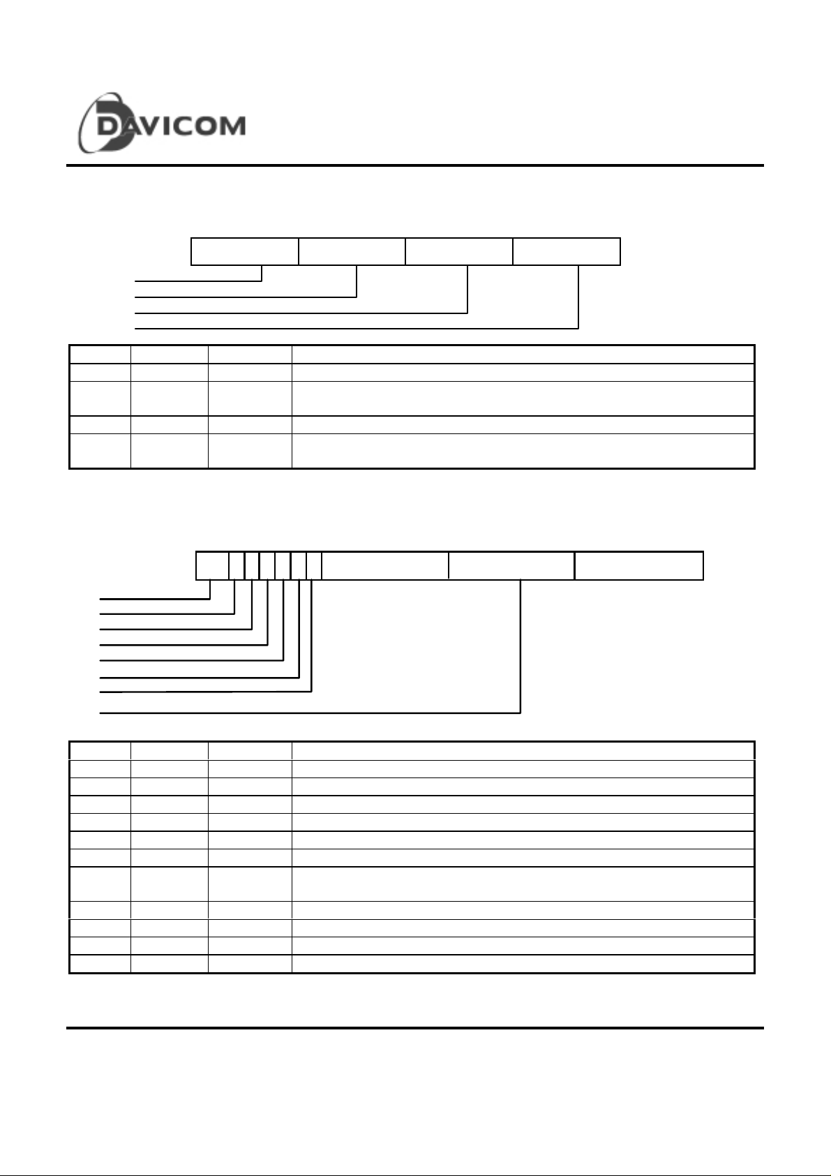
Register Definition
PCI Configuration Registers
The d efiniti o ns of P CI Co nfi gur a tion Registers are based on
the PCI specification revision 2.2 and provides the
initialization and configuration information to operate the PCI
interface in the DM9102A. All registers can be accessed
The default value of PCI configuration registers after reset.
Description Identifier Address Offset Value of Reset
Identification PCIID 00H 91021282H
Command & Status PCICS 04H 02100007H
Revision PCIRV 08H 02000031H
Miscellaneous PCILT 0CH BIOS determine
I/O Base Address PCIIO 10H System allocate
Memory Base Address PCIMEM 14H System allocate
Reserved -------- 18H - 28H 00000000H
CardBus ICS pointer CIS 24H 00000000H
Subsystem Identification PCISID 2CH load from SROM
Expansion ROM Base Address PCIROM 30H 00000000H
Capability Pointer CAP_PTR 34H 00000050H
Reserved -------- 38H 00000000H
Interrup t & L ate nc y PCIINT 3CH Sys te m al locate b it7 ~0
Device Specific Configuration Register PCIUSR 40H 00000000H
Power Management Register PCIPMR 50H C0310001H
Power Management Control & Status PMCSR 54H 00000100H
with byte, word, or double word mode. As defined in PCI
specification 2.1, read accesses to reserve or
unimplemented registers will return a value of “0.” These
registers are to be described in the following sections.
DM9102A
Key to Defa ult
In the register description that follows, the default column
takes the form <Reset Value>
Where
<Reset Value>:
1 Bit set to logic one
0 Bit set to logic zero
X No default value
14 Final
<Access Type>:
RO = Read only
RW = Read/Write
R/C: means Read / Write & Write "1" for Clear.
Version: DM9102A-DS-F03
August 28, 2000
Page 15
Single Chi p Fast E thern et NIC c ont roller
DM9102A
Identification ID (xxxxxx00 - PCIID)
31 16 15 0
Dev_ID
Device ID
Vendor ID
Vend_ID
Bit Default Type Description
16:31 9102h RO The field identifies the particular device. Unique and fixed number for the DM9102A
is 9102h. It is the product nu mber assigned by DAVICOM.
0:15 1282h RO This field identifies the manufacturer of the device. U nique and fixe d n umber f or
Davicom is 1282h. It is a registered number from SIG.
Command & Status (xxxxxx04 - PCICS)
31 16 15 0
Status Command
Status
Command
31 30 29 28 27 26 25 24 23 22 21 20 10
0 0 1 0 0 0191
Detected Parity Error
Signal For System Error
Master Abort Detected
Target Abort Detected
Send Target Abort
DEVSEL Timing
Data Parity Error Detected
Slave mode Fast back to Back
User Definable
66MHz Capability
New Capability
Mast Mode Fast Back-To-Back
SERR# Driver Enable/Disable
Address/Data Steeping
Parity Error Response Enable/Disable
VGA Palette snoop
Memory Write and Invalid
Special Cycle
Master Device Capability Enable/Disable
Memory Space Access Enable/Disable
I/O Space Access Enable/Disable
Reserved
98
76543210
00
00
Final 15
Version: DM9102A-DS-F03
August 28, 2000
Page 16

Bit Default Type Description
31 0 R/C Detecte d Par ity Er ror
The DM9102A samples the AD[0:31], C/BE[0:3]#, and the PAR signal to
ch eck p a rity and t o se t p ar it y e r r ors. I n slav e m od e , t h e pa r i ty c heck falls
on command phase and data valid phase (IRDY# and TRDY# both
active). While in master mode, the DM9102A will check during each data
phase of a me mory read cycle for a parity erro r During a memory write
cycle, if an error occurs, the PERR# signal will be driven by the target. This
bit is set by the DM9102A and cleared by writing "1". There is no effect by
writ ing " 0" .
30 0 R/C Signal For System Error
This bit is set when the SERR# signal is driven by the DM9102A. This
system error occurs when an address parity is detected under the
condition that bit 8 and bit 6 in command register below are set.
29 0 R/C Master Abort Detected
This bit is set when the DM9102A terminates a master cycle with the
master-abort bus transaction.
28 0 R/C Target Abort Detected
This bit is set when the DM9102A terminates a master cycle due to a
target-abort signal from other targets.
27 0 R/C Send Target Abort (0 For No Implementation)
The DM9102A will never assert the target-abort sequence.
26:25 01 R/C DEVSEL Timing (0 1 Se lect Me dium T iming)
Medium timing of DEVSEL# means the DM9102A will assert DEVSEL#
signal two clocks after FRAME# is sample “asserted.”
24 0 R/C Data Pa rity Error Detec ted
This bit will take effect only when operating as a master and when a Parity
Error Response Bit in command configuration register is set. It is set under
two conditions:
(i) PERR# asserted by the DM9102A in memory data read error, (ii)
PERR# sent from the target due to memory data write error.
23 0 RO Slave mode Fast Back-To-Bac k Capable (0 For Not Support)
This bit is always reads "1" to indicate that the DM9102A is capable of
accepting fast back-to-back transaction as a slave mode device.
22 0 RO User-Definable-Feature Supported (0 For Not Support)
21 0 RO 66 MHz Capable (0 For No Capability)
20 1 RO New Capabilities (1 For Good Capability)
This bit indicates whether this function implements a list of extended
capabilities such as PCI power management. When set this bit indicates
the presence of New Capabili tie s. A val u e of 0 means that this funct ion
does not implement New Capabilities.
19:10 0 RO Reser ved
9 0 RO Master Mode Fast Back-To-Back (0 For Not Support)
The DM9102A does not support master mode fast back-to-back capability
and will not generate fast back-to-back cycles.
8 0 RW SERR# Driver Enable/Disable
This bit controls the assertion of SERR# sign al output. The SERR# output
will be asserted on detect ion o f an address parity error and if both this bit
Single Chi p Fast E thern et NIC c ont roller
DM9102A
16 Final
Version: DM9102A-DS-F03
August 28, 2000
Page 17

Single Chi p Fast E thern et NIC c ont roller
and bit 6 are set.
7 0 RO Address/Data Stepping (0 For No Stepping)
6 0 RW Parity Error Response Enable/Disable
Setting this bit will enable the DM9102A to assert PERR# on the detection
of a data parity error and to assert SERR# for reporting address parity
error.
5 0 RO VGA Palette Snooping (0 For Not Support)
4 0 RO Memory Write and Invalid (0 For Not Implementation)
The DM9102A only generates Memory write cycle.
3 0 RO Special Cycles (0 For Not Implementation)
2 1 RW Master Device Capability Enable/Disable
When this bit is set, DM9102A has the a bility of master mode operation.
1 1 RW Memory Space Access Enable/Disable
This bit controls the ability of memory space acc ess. The memory access
includes memory mapped I/O access and Boot ROM access. As the
system boots up, this bit will be enabled by BIOS for Boot ROM memory
access. While in normal operation using memory mapped I/O access, this
bit should be set by driver before memory access cycles.
0 1 RW I/O Space Access Enable/Disable
This bit controls the ability of I/O space access. I t will be set by BIOS after
power on.
DM9102A
Revision ID (xxxxxx08 - PCIRV)
31
Class Code
Class Code
Revision Major Number
Revision Minor Number
Bit Default Type Description
31:8 020000h RO Class Code (020000h)
This is the standard code for Ethernet LAN controller.
7:4 0011 RO Revision Major Number
This is t he s il i co n- ma jo r r evisio n nu m ber that will increase for the subsequent
versions of the DM9102.A.
3:0 0001 RO Revision Minor Number
This is t he s il i co n- m ino r r evisio n nu m ber that will increase for the subsequent
versions of the DM9102A.
4
3
Revision ID
078
Final 17
Version: DM9102A-DS-F03
August 28, 2000
Page 18

DM9102A
Miscellaneous Function (xxxxxx0c - PCILT)
31 16 15 0872324
BIST Header Type Latency Timer Cache Line Size
Built-In Self Test
Header Type
Latency Timer For The Bus Master
Cache Line Size For Memory Read
Bit Default Type Description
31:24 00h RO Built In Self Test ( 00h Means Not Implementation)
23:16 00h RO Header Type ( 00h Means single function with Predefined Header Type )
15:8 00h RW Latency Timer For The Bus Master.
The latency timer is guaranteed by the system and measured by clock cycles.
Wh e n t h e F R A M E# a s s e r t e d a t t h e b e g i n n i n g of a m a s t er pe r i o d by t he D M9102A,
the value will be copied into a counter and start counting down. If the FRAME# is
de-asserted prior to count expiration, this value is meaningless. When the count
expires before GNT# is de-asserted, the master transaction will be terminated as
soon as the GNT# is removed.
While GNT# signal is removed and the counter is non-zero, the DM9102A will
continue with its data transfers until the count expires. The system host will read
MIN_GNT and MAX_LAT registers to determine the latency requirement for the
device and then initialize the latency timer with an appropriate value.
The reset value of Latency Timer is determined by BIOS.
7:0 00h RO Cache line Size For Memory Read Mode Selection ( 00h Means Not
Implementation For Use)
Single Chi p Fast E thern et NIC c ont roller
I/O Base Address (xxxxxx10 - PCIIO)
31 0
I/O Base Address
I/O Base Address
PCI I/O Range
18 Final
I/O or Memory Space Indicator
0000000
1 7 8
1
Version: DM9102A-DS-F03
August 28, 2000
Page 19

Single Chi p Fast E thern et NIC c ont roller
Bit Default Type Description
31:7 Undefined RW PCI I/O Base Address
This is the base address value for I/O accesses cycles. It w ill b e compared to
AD[31:7] in the address phase of bus command cycle for the I/O resource access.
6:1 000000 RO PCI I/O Range Indication
It indicates that the minimum I/O resource size is 80h.
0 1 RO I/O Space Or Memory Space Base Indicator
Determines that the register maps into the I/O space.( = 1 Indicates I/O Base)
Memory Mapped Base Address (xxxxxx14 - PCIMEM)
DM9102A
31
Memory Mapped
Base
Memory Base Address
Memory Range Indication
I/O or Memory Space Indicato r
8
1 7
0000000
Bit Default Type Description
31:7 Undefined R/W PCI Memory Base Address
This is the base address value for Memory accesses cycles. It will be compared to
the AD[31:7] in the address phase of bus command c ycle for the Memo ry r esource
access.
6:1 000000 RO PCI Memory Range Indication
It indicates that the mini mum Mem ory resource size is 80h.
0 0 RO I/O Space Or Memory Space Base Indicator
Determines that the register maps into the memory space( = 0 Indicates Memory
Base)
Subsystem Identification (xxxxxx2c - PCISID)
Subsystem ID Subsystem Vendor ID
Subsystem ID
Subsystem Vendor ID
0
0
031
Bit Default Type Description
31:16 XXXXh RO Subsystem ID
It can be loaded from EEPROM word 1 and different from each card.
15:0 XXXXh RO Subsystem Vendor ID
Unique number given by PCI SIG and loaded from EEPROM word 0.
Final 19
Version: DM9102A-DS-F03
August 28, 2000
Page 20
CardBus CIS Pointer (xxxxxx28 - CCIS)
This Card Information Structure (CIS), also known as tuples,
is a set of data structures saved in a nonvolatile memory on
the CardBus Card. The data stored in CIS describes the
product. Included in this data are the product
manufacturer’s name, product name, and most importantly,
the hardware description. The CIS is supported in the boot
ROM space or the memory space (serial ROM).
CIS is read upon card insertion into the socket. The
software entity that traditio n all y r eads the CIS is usually
known as Card Services and Socket Se rvices (CS & SS).
8
31 03272
ROM Image
Addre ss Space Offset
DM9102A
Single Chi p Fast E thern et NIC c ont roller
The CCIS pointer register is a read-only 32-bit reg ister.
This register points to one of the possible address space
where the card information structure (CIS) begins. The
pointer is used in a CardBus environment. The content of
CCIS is loaded from the serial ROM after a hardware reset.
A value o f 0 in th is re g iste r ind ica tes tha t C IS is n ot
supported.
2
Addre ss Space Indicato r
Bit Default Type Description
31:28 Note R/W ROM Image
The 4- bi t ROM image fiel d value when the CIS reside in an expansion ROM.
27:3 Note R/W Address Space Offset
This field contains the address offset within the address space indicate d b y the
address space indicator field (CCIS<2:0>)
2:0 Note R/W Address Space Indicator
This field indicates the location of the CIS base address. The value of 2 indicates
that the CIS is stored in the serial ROM, and 7, indicates that the CIS is sto re d in the
expansion ROM.
note : read from serial ROM
20 Final
Version: DM9102A-DS-F03
August 28, 2000
Page 21

Expansion ROM Base Address (xxxxxx30 - PCIROM)
DM9102A
Single Chi p Fast E thern et NIC c ont roller
31 01
ROM Base Address
ROM Base Address
18 17
11
0000000
00000000
10
9
Reserved
Bit Default Type Description
31:10 00h RW ROM Base Address With 256K Boundary
PCIROM bit17~10 are hardwired to 0, indicating ROM Size is up to 256K Size
9:1 000000000 RO Reserved Bits Read As 0
0 0 RW Expansion ROM Decoder Enable/Disable
If this bit and the memory space access bit are bot h set to 1, the DM9102A will
responds to its expansion ROM.
Capabilities Pointer (xxxxxx34 - Cap _Ptr)
31
Reserved
0
10100 00
R/W
078
Capability Pointer
Bit Default Type Description
31:8 000000h RO Reserved
7:0 01010000 RO Capability Pointer
The Cap_Ptr provides an offset (default is 50h) into the function’s PCI Configuration
Space for th e loca tion o f the f ir st t er m in th e Capabilitie s Linked List. The Cap_Ptr
offset is DOUBLE WORD aligned so the two least s ignificant bits are always “0”s
Final 21
Version: DM9102A-DS-F03
August 28, 2000
Page 22
DM9102A
Interrupt & Latency Configuration (xxxxxx3c - PCIINT)
31 16 15 0872324
MAX_LAT MIN_GNT INT_PIN INT_LINE
Maximum Latency Timer
Minimum Grant
Interrupt Pin
Interrupt Line
Bit Default Type Description
31:24 28h RO Maximum Latency Timer that can be sustained (Read Only and Re ad As 28h)
23:16 14h RO Minimum Grant
Minimum Length of a Burst Period (Read Only and Read As 14h)
15:8 01h RO Interrupt Pin read as 01h to indicate INTA#
7:0 XXh RW Interrupt Line that Is Routed to the Interrupt Controller
The value depends on mainboard.
Device Specific Configuration Register (xxxxxx40h- PCIUSR)
Single Chi p Fast E thern et NIC c ont roller
3130 29 1615 8 0
Device Specific
Link Event enable/disable
Sample Frame Event enable/disable
Magic Packet Event enable/disable
Link Event Status
Sample Frame Event Status
Magic Packet Event Status
Device Specific
272628
25 24 23
Reserved
7
Reserved
Bit Default Type Description
31 0 RW Device Specific Bit (sleep mode)
30 0 RW Device Specific Bit (snooze mode)
29 0 RW When set enable Link Status Change Wake-up Event
28 0 RW When set enable Sample Frame Wake-up Event
27 0 RW When set enable Magic Packet Wake-up Event
26 0 RO When set, indicates link change and Link Status Change Event occurred
25 0 RO When set, indicates the sample frame is received and Sample Frame Event
occurred
24 0 RO Whe n s e t, i n d ic a t e s th e Ma g i c Pa c k et i s re c e i v ed and Ma g i c p a c k e t E ve n t o cc u r r e d
23:16 00h RO Reserved Bits Read As 0
15:8 00h RW Device Specific
7:0 00h RO Reserved Bits Read As 0
22 Final
Version: DM9102A-DS-F03
August 28, 2000
Page 23

Power Management Register (xxxxxx50h~PCIPMR)
31 16 15 087
PM C Next Item Pointer Capability ID
Power Management Capabilities
Next Item Pointer
Capability Identifier
Bit Default Type Description
31:27 11000 RO PME_Support
These five bits field indicate the power states in which the function may assert
PME#. A value of 0 for any b it indicates that the function i s n o t c apabl e of asserting
the PME# signal while in that power state.
bit27 Æ PME# support D0
bit28 Æ PME# support D1
bit29 Æ PME# support D2
bit30 Æ PME# support D3(hot)
bit31 Æ PME# support D3(cold)
DM9102A’s bit31~27=11000 indicates PME# can be asserted from D3(hot) &
D3(cold).
26:22 00000 RO Reserved (DM9102A not supports D1, D2)
21 1 RO A “1” in d ica t es t ha t th e fun c t ion r eq u ir es a devic e sp ec ific initiali za tion sequence
following transition to the D0 uninitialized state.
20 1 RO Auxiliary Power Source
This b it is o n ly me aning ful i f bi t31 i s a “1 ” .
This bit is “1” in DM9102A indica tes that support for PME# in D3(cold) requires
auxiliary power.
19 0 RO PME# Clock
“0” indicates that no PCI clock is required for the function to generate PME#.
18:16 001 RO Version
A value of 001 indicates that this function complies with the Revision 1.0 of the PCI
Power Management Interface Specification.
A value of 010 is for DM9102A/A that complies with the revision 1.1 of the PC I
Power Management Interface Specification.
15:8 00h RO Next Item Pointer
The offset into the function’s PCI Configuration Space pointing to the location of
next item in the function’s capability list is “00h”
7:0 01h RO Capability Identifier
When “01h” indicates the linked list item as being the PCI Power Management
Registers.
Single Chi p Fast E thern et NIC c ont roller
DM9102A
Final 23
Version: DM9102A-DS-F03
August 28, 2000
Page 24

Power Management Control/Status (xxxxxx54h~PMCSR)
DM9102A
Single Chi p Fast E thern et NIC c ont roller
31
0 0 0 0 0 0 0 0 0 0 0 0 0 0 0 0
PME_Status
16 15 14 9 8 7 2 1 0
R/W 0 0 0 0 0 0 R/W 0 0 0 0 0 0 R/W
PME_En
Power_State
Bit Default Type Description
31:16 0000h RO Reserved
15 0 RW/C PME_Status
This bit is set when the function would normally assert the PME# signal
independent of the state of the PME_En bit. Writing a “1” to this bit will clear it.
This bit defaults to “0” if the function does not support PME# generation from
D3(cold).If the function supports PME# from D3(cold) then this bit is sticky a n d
must be explicitly cleared by the operating sy stem each time the operating
system is initially loaded.
14:9 000000 RO Reserved.
It means that the DM9102A does not s upport reporting power consumption.
8 1 RW PME_En
Write “1” to enables the function to assert PME#, write “0” to disable PME#
assertion.
This bit defaults to “0” if the function does not support PME# generation from
D3(cold).
If the function supports PME# from D3(cold) then this bit is sticky and must be
explicitly cleared by the operating system each time the operating system is
initia lly loaded.
7:2 000000 RO Reserved
1:0 00 RW This tw o bits field is both used to d et ermine the current power sta te of a function
and to set the function into a new power state. Th e definitions given below.
00 : D0
11 : D3(hot)
24 Final
Version: DM9102A-DS-F03
August 28, 2000
Page 25

Control and Status Registers (CR)
DM9102A
Single Chi p Fast E thern et NIC c ont roller
The DM9102A implements 16 control and status registers,
which can be accessed by the ho st. The se CR s a re double
long word aligned. All CRs are set to their default values by
Register Description Offset from CSR
CR0 System Control Register 00H FEC00000
CR1 Transmit Descriptor Poll Demand 08H FFFFFFFF
CR2 Receive Descriptor Poll Demand 10H FFFFFFFF
CR3 Receive Descriptor Base Address Register 18H 00000000
CR4 Transmit Descriptor Base Address Register 20H 00000000
CR5 Network Status Report Register 28H FC000000
CR6 Network Operation Mode Register 30H 02040000
CR7 Interrupt Mas k Register 38H FFFE0000
CR8 Statistical Counter Reg ister 40H 00000000
CR9 External Management Access Register 48H 044097FF
CR10 Programming ROM Address Register 50H Unpredictable
CR11 General Purpose Timer Register 58H FFFE0000
CR12 PHY Status Register 60H FFFFFFXX
CR13 Sample Frame Access Register 68H XXXXXX00
CR14 Sample Frame Data Register 70H Unpredictable
CR15 Watchdog And Jabber Timer Register 78H 00000000H
hardware or software reset unless otherwise specified. A ll
Control and Status Registers with their definitions and offset
from IO or memory Base Address are shown below:
Default va lue
Base Address
after reset
Key to Defa ult
In the register description that follows, the default column
takes the for m:
<Reset Value>, <Access Type>
Where
<Reset Value>:
1 Bit set to logic one
0 Bit set to logic zero
X No default value
Final 25
Version: DM9102A-DS-F03
August 28, 2000
<Access Type>:
RO = Read only
RW = Read/Write
RW/C = Read/Write and Clear
WO = Wr it e on ly
Reserved bits are shaded and should be written with 0.
Reserved bits are undefined on read access.
Page 26

1. System Control Register (CR0)
DM9102A
Single Chi p Fast E thern et NIC c ont roller
31
29 28 27 26
30
25 24 23
22 21
2019181716 151413 121110
987654 321
Bit Name Default Description
24:22 Reser ved 0,RO Reserved
21 MRM 0,RW Memory Read Multiple
When set, the DM9102A will use memory read multiple command (C/BE3~0 =
1100) when it initialize the memory read burst transaction as a master device.
When reset, it will use memory read command (C/BE3 ~ 0 = 0110) for the same
master operation.
20 Reserved 0,RO Reserved
19:17 TXAP 000,RW Transmit Automatic polling interval time
When set, the DM9102A will poll transmit descriptor automatically when it is in the
suspend state due to buff er unavailable. T he p o l ling interv al tim e is program mable
based on the table shown below.
Bit 19 Bit 18
0 0 0 No polling
0 0 1 200us
0 1 0 800us
0 1 1 1.6ms
1 0 0 12.8us
1 0 1 25.6us
1 1 0 51.2us
1 1 1 102.4us
16 Reserved 0,RO Reserved
15:14 ABA 00,RW Address Boundary Alignment
When set, the DM9102A will execute each burst cycles to stop at the programmed
address boundary. The address boundary can be progra m me d t o b e 8 , 16, or 32
doubleword as shown below.
Bit 17 Time Interval
0
Bit 15 Bit 14
Ali gnment Boundar y
0 0 Reserved
0 1 8-double word
1 0 16-double word
1 1 32-double word
13:8 BL 000000,RWBurst Length
When reset, the DM9102A’s burst length in one DM A transfer is limited by the
amount of data in the receive FIFO ( w hen receive ) or the a mount o f free space in
the transmit FIFO (when transmit ). When set, the DMA’s burst length is limited by
the programmed value. The permissib le val ues are 0, 1, 2 , 4, 8 , 16, or 32
doublewords.
7 Reserved 0,RO Reserved
6:2 Reserved 00000
1 Reserved 0,RO Reserved
26 Final
Version: DM9102A-DS-F03
August 28, 2000
Page 27

Single Chi p Fast E thern et NIC c ont roller
Bit Name Default Description
0 SR 0,RW Softwar e Res et
When set, the DM9102A will make a internal reset cycle. All consequent action to
DM9102A2 should wait at least 32 PCI clock cycles to start and no necessary to
rese t th is b it.
2. Transmit Descriptor Poll Demand (CR1)
DM9102A
31 30
29 28 27
26
25 24
22
21 20
23
19 18 17 161514 13 12 11
10
987
Bit Name Default Description
31:0 TDP FFFFFFFFh
,WO
Transmit Descriptor Polling Command
Writing any value to this port will force DM9102A to poll the tran smit d e sc riptor. If
the acting descriptor is not a vailable, transmit process will return to suspend state.
If the descriptor shows buffer available, transmit process will begin the data
transfer.
3. Receive Descriptor Poll Demand (CR2)
31 30
29 28 27
26
25 24
22
21 20
23
19 18 17 161514 13 12 11
10
987
Bit Name Default Description
31:0 RDP FFFFFFFFh
,WO
Receive Descriptor Polling Command
Writing any value to this port will force DM9102A to poll the receive descriptor. If the
act ing d e scri p tor is no t a v ailabl e, r ec eiv e process will r eturn to suspend state. If the
descriptor shows buffer available, receive process will begin the data transfer.
6
54321
6
54321
0
0
4. Receive Descriptor Base Address (CR3)
31 30
29 28 27 26
25 24 23
22 21
2019181716 151413 12
10
11
9 8 7 6 5 4 3 2 1
0
0000
Bit Name Default Description
31:0 RDBA 00000000h
,RW
Receive Descriptor Base Address
This register defines base address of receive descriptor-chain. The receive
descriptor- polling command after CR3 is set w ill make DM9102A to fetch the
descriptor at the Base-Address.
Final 27
Version: DM9102A-DS-F03
August 28, 2000
Page 28

Single Chi p Fast E thern et NIC c ont roller
5. Transmit Descriptor Base Address (CR4)
31 30
29 28 27 26
25 24 23
22 21
2019181716 151413 12
10
11
9 8 7 6 5 4 3 2 1
Bit Name Default Description
31:0 TDBA 00000000h,RWTransmit Descriptor Base Address
This register defines base address of transmit d escriptor-chain. The tran smit
descriptor- polling command after
CR4 is set will make DM9102A to fetch the descriptor at the Base-Address.
6. Network Status Report Register (CR5)
DM9102A
0
0000
31
29 28 27 26
30
25 24 23
22 21
2019181716 151413 121110
987654 321
Bit Name Default Description
25:23 SBEB 000,RO System Bus Error Bits
These bits are read only and used to indicate the type of system bus fetal error. Valid
only when System Bus Error is set. The mapping bits are shown belo w.
Bit25 Bit24
Bit23 Bus Error Type
0 0 0 Parity error
0 0 1 Master abort
0 1 0 Slave abort
0 1 1 Reserved
1 X X Reserved
22:20 TXPS 000,RO Transmit Process State
These bits are read only and used to indicate the state of transmit process.
The mapping table is shown belo w.
Bit22 Bit21
Bit20 Process State
0 0 0 Transmit process stopped
0 0 1 Fetch transmit descriptor
0 1 0 Move Setup Frame from the host memory
0 1 1 Move data from host memory to transmit FIFO
1 0 0 Close descriptor by clearing owner bit of descri ptor
1 0 1 Waiting end of transmit
1 1 0 Transmit end and Close descriptor by writing status
1 1 1 Transmit process suspend
19:17 RXPS 000,RO Receive Process State
These bits are read only and used to indicate the state of receive process. The
mapping table is show n below.
Bit19 Bit18
Bit17 Process State
0 0 0 Receive process stopped
0 0 1 Fetch receive descriptor
0 1 0 Waiting for receive packet under buffer availabl e
0 1 1 Move data from receive FIFO to host memor y
0
28 Final
Version: DM9102A-DS-F03
August 28, 2000
Page 29

1 0 0 Close descriptor by clearing owner bit of descripto r
1 0 1 Close descriptor by writing status
1 1 0 Receive process suspended due to buffer un avail able
1 1 1 Pur ge t he cu rrent frame from the receive FIFO
because o f unavailable receive buffer
16 NIS 0,RW Normal Interrupt Summary
Normal interrupt includes any of the th ree con ditions :
CR5<0> – TXCI : Transmit Complete Interrupt
CR5<2> – TXDU : Transmit Buffer Unavailable
CR5<6> – RXCI : Receive Complete Interrupt
15 AIS 0,RW Abnormal Interrupt Summary
Abnormal interrupt includes any interrupt condition as shown below excluding Normal
Interrupt conditions. They are TXPS(bit1), TXJT(bit3), TXFU(bit5), RXDU(bit7),
RXPS(bit8), RX WT(bit9), TXER(b it10), GPT( bit11), SBE(bit13 ).
14 ERI 0,RW Early Receive Interrupt
This bit will be set when early receive interrupt has happened.
13 SBE 0,RW System Bus E rror
The PCI system bus errors w ill set this bit. The type of s ystem bus error is shown in
CR5<25:23>.
12 LCI 0,RW Link Status Change Interrupt
This bit will be set when link status change.
11 GPT 0,RW General-purpose Timer Expired
This bit is set to indicate the gener al-purpose timer (described in CR11) has expired.
10 TXER 0,RW Transmit Early Interrupt
Transmit Early Interrupt is set when the full packet data has been moved from host
memory into transmit FIFO. It will inform the host to process ne xt step before the
trans miss ion end. Tra n smi t complete eve n t CR5 <0> w i l l cle ar this bit auto m a tically.
9 RX WT 0,RW Receive Watchdog Timer Expired
This bit is set to indicate receive watchdog timer has expired.
8 RXPS 0,RW Receive Process Stopped
This bit is set to indicate receive process enters the stopped state.
7 RXDU 0,RW Receive Bu ffe r U navailable
This bit is set when the DM9102A fetches the next receive descriptor that is still
owned by the host. Recei ve process will be suspended until a new frame enters or
the receive polling command is set.
6 RXCI 0,RW Receive Co mp lete Inte r rup t
This bit is set when a rec eived frame is fully moved into host memory and receive
status has been written to descriptor. Receive process is still running and continues to
fetch next descriptor.
5 TXFU 0,RW Transmit FIFO Underrun
This bit is set when transmit FIFO has underrun condition during the packet
transmission. It may happen due to the h eavy load on bus, receive process
dominates in full-duplex operation, or transmit buffer unavailable before end of
packet. In this case, transmit process is placed in the suspend state and underrun
error TDES0<1 > is set.
3 TXJT 0,RW Transmit Jabber Timer Expired
This bit is set when the jabber timer expired with the transmitter is still active.
Transmit process will be aborted and placed in the stop state. It also causes transmit
jabber timeout TDES0<14> to assert.
2 TXDU 0,RW Transmit Bu ffe r U na va ilab le
DM9102A
Single Chi p Fast E thern et NIC c ont roller
Final 29
Version: DM9102A-DS-F03
August 28, 2000
Page 30

This bit is set when the DM9102A fetches the next transmit descriptor that is still
owned by the host. Transmit process will be suspended until the transmit polling
command is set or auto-polling timer time-out.
1 TXPS 0,RW Transmit Process Stopped
This bit is set to indicate transmit process enters the stopped state.
0 TXCI 0,RW Trans mi t Co mp lete In terru p t
This bit is set when a frame is fully transmitted and transmit status has been written to
descriptor (the TDES1<31> is also asserted). Transmit proces s is still running and
continues to fetch next descriptor.
7. Network Operation Mode Register (CR6)
DM9102A
Single Chi p Fast E thern et NIC c ont roller
313029 28 27 26
25 24 23
22 21
2019181716 151413 121110
000 11 0000 0
0
987654 321
Bit Name Default Description
30 RXA 0,RW Receive All
When set, all incoming packet will be received, regardless the destination address.
The address match is checked according to theCR6<7>, CR6<6>, CR6<4>,
CR6<2>, CR6<0>, and RDES0<30> will show this match.
29 NPFIFO 0,RW Set to not purge RX FIFO if RX buffer unavailable
28:26 Reserved 000,RO Must be Zero
25 Reserved 1,RO Must be One
24:23 Reserved 00,RO Must be Zero
22 TXTM 1,RW Transmit Threshold Mode
When set, the transmit threshold mode is 10Mb/s. When reset, the threshold mode
is 100Mb/s. This bit is used together with CR6<15:14> to decide the e xact
threshold level.
21 SFT 0,RW Store and Forward Transmit
When se t, th e packe t t ra nsmissi on from MAC will be started after a full frame has
been moved from the host memory to transmit FIFO. When reset, the packet
transmission’s start will depend on the threshold value specified in CR6<15:14>
20 STI 0,RW Start Transmission Immediately
When th is b it is s et , th e packe t t rans mi ssi o n fro m MAC wi ll be s ta r te d im me diat ely
after transmit FIFO’s threshold level reaches 16 b ytes, regardless of the setting in
CR6<22> and CR6<15:14>. This mode will make transmit FIFO underrun
condition to happen more easily.
19 Reserved 0,RO Reser ved
18 External
MII_Mo de
1,RW 1: Se lec t e xte rna l MI I inter fac e .
0: Select external SRL interface.
In external MII mode that the pins TEST1, TEST2, and CLOCKRUN# are forced to
low, the DM9102A bypasses internal PHY and uses external PHY, by setting this
bit properly.
Se e page 66 for d etails.
17 Reserved 0,RO Reser ved
16 1pkt 0,RW One Packet Mode
When this bit is set, only one packet is stored at TX FIFO.
0
30 Final
Version: DM9102A-DS-F03
August 28, 2000
Page 31

15:14 TSB 0,RW Threshold Bits
These bits are set tog ether with CR6<22> (chose 10Mb or 100Mb) and will decide
the exact FIFO threshold level. The packet transmission will s t a r t after the data level
exceeds the threshold value.
Bit15 Bit14
0 0 128 72
0 1 256 96
1 0 512 128
1 1 Reserved Reserved
13 TXSC 0,RW Transmit Start/stop Command
When set, transmit process will begin by fetching the transmit descriptor for
available packet data to be transmitted (running state). If the fetched de scriptor is
owned by the host, transmit process will enter the suspend state and transmit buffer
unavailable (CR5<2>) is set. Otherwise it will begin to move data from host to
FIFO and transmit out after reaching threshold level.
When reset, transmit process is placed in the stopped state after completing the
transmission of the current frame.
12 FCM 0,RW Force Collision Mode
When set, the transmission process is forced to be the collision status. Meaningful
only in the internal loopback mode.
11:10 LBM 0,RW Loopback Mode
These bits de cide two loopback modes besides normal operation. External
loopback mode expects transmitted data back to receive path and makes no
collis ion det ecti on.
Threshold(100M) Threshold(10M)
DM9102A
Single Chi p Fast E thern et NIC c ont roller
Bit11 Bit10
0 0 normal
0 1 internal l oopback
1 0 int ernal PHY digital l oopback
1 1 internal PHY analog loopback
9 FDM 0,RW Full-duplex Mode
This bit is set to make DM9102A operate in the full-duplex mode. Transmit and
receive processes can work simultaneously.
There is no collision detection needed during this mode operation.
8 Reserved 0,RO Must be zero.
7 PAM 0,RW Pass All Mu lticast
When set, any packet with a multicast destination address is received by the
DM9102A. The packet with a physical address will also be filtered based on the
filter mode setting.
6 PM 1,RW Promiscuous mode
When set, any incoming valid frame is received by the DM9102A, and no matter
what the destination address. The DM9102A is initialized to this mode after reset
operation.
5 Reserved 0,RO Must be Zero.
4 IAFM 0,RO Inverse Address Filtering Mode
It is se t to in dic ate the DM9102A operate in a Inverse Filtering Mode. This is a read
only bit and mapped from the setup frame together with CR6<2>, CR6<0> setting.
Th at i s , i t i s val i d only d uri ng pe rfect f i l teri n g mode.
Loopback Mode
Final 31
Version: DM9102A-DS-F03
August 28, 2000
Page 32

3 PBF 0,RW Pass Bad Fra me
When set, the DM9102 is indicated to receive the bad frames including runt
packets, truncated frames caused by the FIFO overflow. The bad frame also has to
pass the address filtering if the DM9102A i s not set in promiscuous mode.
2 HOFM 0,RO Hash-only Filter Mode
This is a read-only bit and mapped from the set-up frame together with bit4,0 of
CR6.
It is se t to in dic ate the DM9102A operate in a Hash-only Filtering Mode.
1 RXRC 0,RW Receive Start/Stop Command
When set, receive process w ill begin by fetching the receive descriptor for availabl e
buffer to store the new-coming packet (placed in the running stat e) . If the fetched
descriptor is owned by the host (no descriptor is owned by the DM9102A), the
receive process will enter the suspend state and receive buffer unavailable
CR5<7> sets. Otherwise it runs to wait for the packet’s income. When reset,
receive process is placed in the stopped state after completing the reception of the
current frame.
0 HPFM 0,RO Hash/Perfect Filter Mode
This is a read only bit and mapped from the setup frame together with CR6<4>,
CR6<2>. When reset, the DM9102A does a perfect address filter of incoming
frames according to the addresses specified in the setup frame. When set, the
DM9102A does a imperfect address filtering for the incoming frame with a multicast
address according to the hash table specified in the setup frame. The filte ring mode
(perfect / imperfect) for the frame with a physical address will depend on CR6<2>.
DM9102A
Single Chi p Fast E thern et NIC c ont roller
8. Interrupt Mask Register (CR7)
31
29 28 27 26
30
25 24 23
22 21
2019181716 151413 121110
987654 321
Bit Name Default Description
16 NISE 0,RW Normal Interrupt Summary Enable
This bit is set to enable the interrupt for Normal Interrupt Summary.
Normal interrupt includes three conditions :
CR5<0> – TXCI : Transmit Complete Interrupt
CR5<2> – TXDU : Transmit Buffer Unavailable
CR5<6> – RXCI : Receive Complete Interrupt
15 AISE 0,RW Abnormal Interrupt Summary Enable
This bit is set to enable the interrupt for Abnormal Interrupt Summary.
Abnormal interrupt includes all interrupt condition as shown below excluding
Normal Interrupt conditions. They are TXPS(bit1), TXJT(bit3), TXFU(bit5),
RXDU(bit7), RX PS(bit8) , RXWT(bit9), TXER(bit10) , GPT(bit11), SB E(bit13).
14 ERIE 0,RW Early Receive Interrupt Enable
This bit is set to enable the interrupt for Early Receive.
13 SBEE 0,RW System Bus Error Enable
When set together with CR7<15>, CR5<13>, it enables the interrupt for System
Bus Error. The type of system bus error is shown in CR5<24:23>.
12 LCIE 0,RW Link Status Change Interrupt Enable
This bit is set to enable the interrupt for link status change.
0
32 Final
Version: DM9102A-DS-F03
August 28, 2000
Page 33

11 GPTE 0,RW General-purpose Timer Expired Enable
This bit is set together with CR7<15>, CR5<11> then it will enable the interrupt for
the condition of the general-purpose timer (described in CR11) expired.
10 TXERE 0,RW Transmit Early Interrupt Enable
This bit is set together with CR7<16>, CR5<10> then it enables the interrupt of the
early transmit event.
9 RX WTE 0,RW Receive Watchdog Timer Expired Enable
When this bit and CR7<15>, (CR5<9> are set together, it enable the interrupt of the
condition of the receive watchdog timer expired.
8 RXPSE 0,RW Receive Process Stopped Enable
When set together with CR7<15> and CR5<8> . T hi s bit is set to enable the
interrupt of receive process stopped condition.
7 RXDUE 0,RW Receive Buffer Unavailable Enable
When this bit and CR7<15>, CR5<7> are set together, it w ill enable the interrupt of
receive buffer unavailable condition.
6 RXCIE 0,RW Re cei ve C o mplete In te rru pt En ab le
When this bit and CR7<16>, CR5<6> are set together, it w ill enable the interrupt of
receive process complete condition.
5 TXFUE 0,RW Transmit FIFO Underrun Enable
When set together with CR7<15>, CR5<5>, it wil l enabl e the i nterrupt of transmit
FIFO underrun condition.
4 Reserved 0,RO Reserved
3 TXJTE 0,RW Transmit Jabber Timer Expired Enable
When this bit and CR7<15>, CR5<3> are set together, it enables the interrupt of
transmit Jabber Timer Expired condition.
2 TXDUE 0,RW Transmit Buffer Unavailable Enable
When this bit and CR7<16>, CR5<2> are set together, transmit bu ffer unavailable
interrupt is enabled.
1 TXPSE 0,RW Transmit Process Stopped Enable
When this bit is set together with CR7<15> and CR5<1>, it will enable the interrupt
of the transmit process stopped
0 TXCIE 0,RW Trans mit C o mple te Inte rrup t E nab le
When this bit and CR7<16>, CR5<0> are set, the tra n smit i nterrupt is enabled.
DM9102A
Single Chi p Fast E thern et NIC c ont roller
9. Statistical Counter Register (CR8)
31 30
29 28 27
26
25 24
22
21 20
23
19 18 17 161514 13 12 11
10
987
6
54321
0
Bit Name Default Description
31 RXFU 0,RO Receive Overflow Counter Overflow
This bit is set when the Purged Packet Counter (RXDU) has an o v erflow condition.
It is a read only register bit.
30:17 RXDU 0,RO Receive Purged Packet Counter
This is a statistic counter to ind icate the purged rec eived pa cket count upon FIFO
overflow.
Final 33
Version: DM9102A-DS-F03
August 28, 2000
Page 34

16 RXPS 0,RO Receive Missed Counter Overflow
This bit is set when the Receive Missed Frame Counter (RXCI) has an o verflow
condition. It is a read only register bit.
15:0 RXCI 0,RO Receive Missed Frame Counter
This is a statistic counter to indicate the Receive Missed Frame Count when there is
a host buffer unavailable condition for receive process.
10. PROM & Management Access Register (CR9)
DM9102A
Single Chi p Fast E thern et NIC c ont roller
31 30
29 28 27
26
25 24
22
21 20
23
19 18 17 161514 13 12 11
10
987
6
54321
Bit Name Default Description
31:22 Undefined X,RO Undefined
21 LES 0,RO Load EEPROM status
It is s et t o in di cate th e loa d of EEP RO M is fini s hed.
20 RLM 0,RW Reload EEPROM
It is set to reload the content of EEPROM.
19 MDIN 0,RO MII Management Data_In
This is read only bit to indicate the MDIO input data.
18 MRW 0,RW MII Management Read/Write Mode Selection
This bit defines the Read/Write Mode for MII management interface for PHY
access.
17 MDOUT 0,RW MII Management Data_Out
This bit is used to generate the output data signal for the MDIO pin.
16 MDCLK 0,RW MII Management Clock
This bit is used to generate the output clock signal for the MDC pin.
15 MBO 1,RO Must be One.
14 MRC 0,RW Memory Read Control
This bit is set to perform the read oper ation for the Boot PROM o r EEPROM
access.
13 EWC 0,RW Memory Write Control
This bit is set to perform the write operation for the Boot PROM (Multiplex mode) or
EEPROM acces s.
12 BRS 1,RW Boot ROM Selected
This b it is s e t to se lect th e Boo t RO M a c ces s for me mory interface.
11 ERS 0,RW EEPROM Selected
This b it is s e t to se lect th e EE PRO M a c ces s for me mory interface.
10 XRS 1,RW External Register Selected
This b it is s e t to se lect a n e xtern a l reg is ter.
9:8 MBO 1,RO Must be One
7:0 DATA 1,RW Data input/output of Boot ROM
This field contains the data which reads from or write to the Boot ROM w hen the
Boot ROM mode is selected. ( CR9<12> = 1 )
If EEPROM is selected ( CR9<11> = 1 ), then CR9<3:0> are connected the ser ial
ROM control pins.
0
34 Final
Version: DM9102A-DS-F03
August 28, 2000
Page 35

3 CRDOUT 1,RW Data_Out from EEPROM
This bit is set to re flect the sign al status of EEDI pin when EEPROM mode is
selected.
2 CRDIN 1,RW Data_In to EEPROM
This bit is set to generate the output sign al to E E DO pin when EEPRO M mode is
selected.
1 CRCLK 1,RW Clock to EEPROM
This bit is set to generate the output clock t o EECLK pin when EEPROM mode is
selected.
0 CRCS 1,RW Chip_Select to EEPROM
This bit is set to generate the output sign al to EEC S pin when EEPROM mode is
selected.
11. Programming ROM Address Register (CR10)
DM9102A
Single Chi p Fast E thern et NIC c ont roller
31 30
29 28 27
26
25 24
22
21 20
23
19 18 17 161514 13 12 11
10
987
6
54321
Bit Name Default Description
17:0 BADR Unpredictable Boot ROM Address
This field contains the address pointer for Boot ROM when the mode of
programming by register is selected.
12. General Purpose Timer Register (CR11)
29 28 27
31 30
26
25 24
22
21 20
23
19 18 17 161514 13 12 11
10
987
6
54321
0
Bit Name Default Description
16 TCON 0,RW Continuous Mode of Timer
When this b it is set, th e timer will co ntinuously re-initiated upon the set time is up.
When reset, the timer will be one-shot response after BCLK value is programmed.
15:0 MBCLK 0000h,RW Multiple of Base Clock
This field set the iteration number of base clock. The base clock duration is defined
to be
81.92us --- for MII port/100M is selected
2us --- for M II port/10 M is s elec ted
0
13. PHY Status Register (CR12)
29 28 27
31
30
26
25 24 23
22 21 20
191817
15
16
14
13 12
10
11
987654321
0
Bit Name Default Description
Final 35
Version: DM9102A-DS-F03
August 28, 2000
Page 36

Single Chi p Fast E thern et NIC c ont roller
8 GEPC X,R W GEPD Bits Control
When in in it ia liza tio n , thi s bit i s set and the unique “80h” must be written to the
GEPD(7:0). After initialization, this bit is reset and it controls the functional mode of
GEPD in bit0~7.
7 GEPD(7) X,RW General PHY Reset Control
It must be s et to “1” if CR12 <8> is set.
When CR12<8> is reset, write “1” to this bit will reset the PHY of the DM9102A.
6:0 GEPD(6:0) XXXXXXX
,RW
General PHY Status
When CR12<8> is set at initialization, it operates the only write operati on and write
the unique “0000000” to these seven bits.
After initialization, CR12<8> is reset, write operation is meaningless and read
these seven bits to indicate the PHY status.
These status bits are shown belo w.
bit 6:Current Media Link Status
bit 5:Signal Detection
bit 4:RX-lock
bit 3:Internal PHY Link status (the same as bit2 of PHY Register)
bit 2:Full-duplex
bit 1:Speed 100Mbps link
bit 0:Speed 10Mbps link
14. Sample Frame Access Register (CR13) (reference to Power Management section)
DM9102A
31
29 28 27 26
30
25 24 23
22 21
2019181716 151413 121110
987654 321
register general definition bit8 ~ 3 R/W
TxFIFO transmit FIFO access port 32h R/W
RxFIFO receive FIFO access port 35h R/W
DiagReset general reset for diagnostic pointer port 38h W
15. Sample Frame Data Register (CR14) (reference to Power Management section)
22 21
31
29 28 27 26
30
25 24 23
2019181716 151413 121110
987654 321
16. Watchdog and Jabber Timer Re gister (CR15)
31
29 28 27 26
30
25 24 23
22 21
2019181716 151413 121110
987654 321
Bit Name Default Description
31:25 Reserved 0,RO Reserved
0
0
0
36 Final
Version: DM9102A-DS-F03
August 28, 2000
Page 37

24:22 ERIT 000,RW Early Receive Interrupt Threshold
These three bits determine the threshold of the received packet data from RX FIFO
to host memory.
bit24 bit 23 bit22 threshold (perc entage)
0 0 0 Disable
0 0 1 12.5%
0 1 0 25.0%
0 1 1 37.5%
1 0 0 50.0%
1 0 1 62.5%
1 1 0 75.0%
1 1 1 87.5%
DM9102A
Single Chi p Fast E thern et NIC c ont roller
21:16 FIFOT 000000
,RW
15 TXPM 0,RW Transmit pause packet condition control
14 TXP0 0,RW Transmit pause packet
13 TXPF 0,RW Transmit pause packet
12 TXPE1 0,RW Transmit pause packet enable
11 TXPE2 0.RW Transmit pause packet enable
10 FLCE 0,RW Flow Control Enable
9 RXPS 0,R/C The latched status of the decode of the pause packet.
8 Reserved 0,RO Reserved.
7 RXPCS 0,RO Of the decode of the pause packet.
6 VLAN 0,RW VLAN Capability Enable
5 TWDR 0,RW Time Interval of Watchdog Release
4 TWDE 0,RW Watchdog Timer Disable
3 Reserved 0,RO Reserved
RX FIFO flow control threshold option
The value of bit21~16 determine the threshold of RX FIFO overflow when in flow
control mode. The exact threshold is 32bytes multiplied by this value.
1 = Indicate Transmit pause packet either CR15<11> or CR15<12> is set.
0 = Indicate Transmit pause packet both CR15<11> and CR15<12> are set.
Set to Transmit pause packet with pause timer = 0000h
Set to Transmit pause packet with pause timer = FFFFh, this bit will be cleared if
packet had transmitted.
Set to enable T ransmit pause packet if descriptor unavailable
Set to enable T ransmit pause packet with time = FFFFh if FIFO near o verflow, or
with time = 0000h if FIFO empty.
Set to enable the decode of the pause packet.
It is set to enable the VLAN mode.
This bit is used to select the time interval between receive Watchdog timer
expiration until re-enabling of the receive channel. When this bit is set, the tim e
interval is 40~48 bits time. When this bit is reset, it is 16~24 bits time.
When set, the Watchdog Timer is disabled. Otherwise it is enabled.
Final 37
Version: DM9102A-DS-F03
August 28, 2000
Page 38

2 JC 0,RW Jabber Clock
When set, the trans mission is cu t off after a range o f 2048 bytes to 2560 bytes is
transmitted.
When res e ts , tra n smission for the 10Mbps port is cut off after a range of 26ms to
33ms.
When res e ts , tra n smission for the 100Mbps port is cut off after a range of 2.6ms to
3.3ms.
1 TUNJ 0,RW Transmit Unjabber Interval
This bit is used to select the time interval between trans mit jabber timer e xpira tion
until re-enabling of the transmit channel. When set, transmit channel is released
right after the jabber expiration. When reset, the time interval is 365~420ms for
10Mb/s port and 36.5~42.0ms for 100Mb/s.
0 TJE 0,RW Transmit Jabber Disable
When set, the transmit Jabber Timer is disabled. Otherwise it is enabled.
DM9102A
Single Chi p Fast E thern et NIC c ont roller
38 Final
Version: DM9102A-DS-F03
August 28, 2000
Page 39

CardBus S tatus Ch ang ed R egister s
DM9102A
Single Chi p Fast E thern et NIC c ont roller
The DM9102A implements four status changed registers.
These status changed registers are accessed by the
CardBus systom software. These registers are mapped
1. Function Event Register: (offset 80h)
Bit Name Default Description
0:3 Reser ved R/W Unpredictable on read
4 General Wake-up
Event
5:14 Reserved R/W Unpredictable on read
15 Interrupt R/WC This bit is set when there is an interrupt pending.
16:31 Reserved R/W Unpredictable on read
2. Function Event Mask Register: (offset 84h)
Bit Name Default Description
0:3 Reser ved R/W Unpredictable on read
R/WC This bit is set w hen the DM9102A has detected a power management event.
This bit is cleared upon power-up reset and by write 1. It is unaffected by either
hardware or software reset. When the PME_Status bit in the PCI configuration is
cleared, this bit is automatically cleared as well.
This b it is c le a re d b y wri t e 1 . This bit is cleared upon har dware or software reset.
only to the memory address space and not to the I/O
address space.
4 General Wake-up
Event Enable
5:13 Reserved R/W Unpredictable on read
14 Wake-up Event
Summary Enable
15 Interrupt Re g iste r
Enable
16:31 Reserved R/W Unpredictable on read
3. Function Present State Register: (offset 88h)
Bit Name Default Description
0:3 Reser ved R/W Unpredictable on read
Final 39
Version: DM9102A-DS-F03
August 28, 2000
R/WC When set together with the Wake-up Event Summary Enable bit (Function Event
Mask Register<14>), enables the assertion of the CSTSCHG pin.
To disable the assertion of the CSTSCHG, the PME_Enable bit in the PCI
con figura t ion r eg ist er (PM C<8>) mu st b e cl ear e d as well.
This bit is cleared upon power up reset.
R/W When set together with the General Wake-up Event Enable bit (Function Event
Mask Register<4>), enables the assertion of the CSTSCHG pin.
To disable the assertion of the CSTSCHG pin, the PME_Enable bit in the PCI
con figura t ion r eg ist er (PM C<8>) mu st b e cl ear e d as well.
This is cleared upon power up reset.
R/W When set, enable the assertion of the interrupt pin (INT#).
This bit is cleared upon hardware o r software reset.
Page 40

DM9102A
Single Chi p Fast E thern et NIC c ont roller
4 General Wake-up
Event
5:14 Reserved R/W Unpredictable on read
15 Interrupt R This bit reflects the internal state of a function specific interrupt. It is cleared when
16:31 Reserved R/W Unpredictable on read
4. Function Force Event Register: (offset 8Ch)
Bit Name Default Description
0:3 Reser ved R/W Unpredictable on read
4 Force Wake-up W Writing 1 to this bit sets the wake-up event field in the Function Event Register
5:14 Reserved R/W Unpredictable on read
15 Forc e Int er r up t W Writ in g 1 to t h is b it s e ts th e in ter ru p t f ield i n the Function Event Register (Function
16:31 Reserved R/W Unpredictable on read
R This bit reflects the current state of the wake-up e vent. It is cleared when either the
General Wake-up Event in the Function Event Register is cleared or when the
PME_Status in the PMC is cleared.
This bit is cleared upon hardware o r software reset.
the event that caused the interrupt was either masked in CSR7, or cleared in
CSR5.
This bit is cleared upon hardware o r software reset.
(Function Event Register<4>), but not in the Function Present State Register
(Function Present State Register<4>).
Writing 0 has no effect.
Event Register<15>), but not in the Function Present State Register (Function
Present State Register<15>).
Writing 0 has no effect.
40 Final
Version: DM9102A-DS-F03
August 28, 2000
Page 41

Single Chi p Fast E thern et NIC c ont roller
DM9102A
PHY Management Registers
Offset Register Name Description Default value after reset
0 BMCR Basic Mode Control Register 3100h
1 BMSR Basic Mode Status Register 7809h
2 PHYIDR1 PHY Identifier Register #1 0181h
3 PHYIDR2 PHY Identifier Register #2 B840h
4 ANAR Auto-Negotiation Advertisement Register 01E1h
5 ANLPAR Auto-Negotiation Link Partner Ability Register 0000h
6 ANER Auto-Negotiation Expansion Register 0000h
7-15 Reser ved Reserved 0000h
10h DSCR DAVICOM Specified Configuration Register 0000h
11h DSCSR DAVICOM Specified Configuration/Status Register F010h
12h 10BTCSR 10BASE-T Configuration/Status Register 7800h
Others Reserved Reserved for future use, do not Read/Write to these
Registers
Key to Defa ult
0000h
In the register description that follows, the default column
takes the for m:
<Reset Value>, <Access Type> / <Attribute(s)>
Where
<Reset Value>:
1 Bit set to logic one
0 Bit set to logic zero
X No default value
(PIN#) Value latched in from pin # at reset
<Access Type>:
RO = Read only
RW = Read/Write
<Attribute (s )>:
SC = Self clearing
P = Value permanently set
LL = Latching low
LH = Latching high
Final 41
Version: DM9102A-DS-F03
August 28, 2000
Page 42

Basic Mode Control Register (BMCR) – 0
Bit Name Default Description
0.15 Reset 0, RW/SC Reset:
1=Software reset
0=Normal operation
This bit sets the status and controls the PHY registers of the DM9102A to their
default states. This bit, which is self-clearing, will keep returning a value of one
until the reset process is completed
0.14 Loopback 0, RW Loopback:
1=Loop-back enabled
0=Normal operation
When in 100Mbps operation mode, setting this bit may cause the
descrambler to lose synchronization and produce a 720ms "dead time" before
any valid data appear at the MII receive output s
0.13 Speed Selection 1, RW Speed Select:
1=100Mbps
0=10Mbps
Link speed may be selected either by this bit or by Auto-negotiation. When
Auto-negotiation is enabled and bit 12 is set, this bit w ill return Autonegotiation selected media type.
0.12 Auto-negotiation
Enable
0.11 Power Down 0, RW Power Down:
0.10 Isolate 0,RW Isolate:
0.9 Restart Au tonegotiation
0.8 Duplex Mode 1,RW Duplex Mode:
0.7 Collision Test 0,RW Collision Test:
1, RW Auto-negotiation Enable:
1= Auto-negotiation enabled: bit 8 and 13 will be in A uto -negotiation status
0= Auto-negotiation disabled: bit 8 and 13 will determine the link speed and
mode
Setting this bit willpower down the whole chip except crystal / os cillator circuit.
1=Power Down
0=Normal Operation
1= Isolates the DM9102A from the MII with the exception of the serial
management.
0= Normal Operation
0,RW/SC Restart Auto-negotiation:
1= Restart Auto-negotiation. Re-initiates the Auto-negotiation process. When
Auto-negotiation is disabled (bit 12 of this register cleared), this bit has no
func tion an d it shoul d be cleared. This bit i s se lf- cl e aring and it wi ll keep
returning a value of 1 until Auto-negotiation is initiated by the DM9102A. The
operation of the Auto-negotiation process will not be a ffected by the
management entity that clears this bit.
0= Normal Operation
1= Full Duplex operation. Duplex selection is allowed when Auto-negotiation is
disabled (bit 12 of this register is cleared). With Auto-negotiation enabled, this
bit reflects the duplex capability selected by Auto-negotiation.
0= Normal operation
1= Collision Test enabled. When set, this bit will cause the COL signal to be
asserted in response to the assertion of TX_EN.
Single Chi p Fast E thern et NIC c ont roller
DM9102A
42 Final
Version: DM9102A-DS-F03
August 28, 2000
Page 43

0= Normal Operation
0.6:0.0 Reserved <0000000>,ROReserved. Write as 0, ignore on read
Basic Mode Status Register (BMSR) – 1
Bit Name Default Description
1.15 100BASE-T4 0,RO/P 100BASE-T4 Capable:
1=DM9102A is able to perform in 100BASE-T4 mode
0=DM9102A is not able to perform in 100BASE-T4 mode
1.14 100BASE-TX
Full Duplex
1.13 100BASE-TX
Half Duplex
1.12 10BASE-T
Full Duplex
1.11 10BASE-T
Half Duplex
1.10-1.7 Reserved 0000,RO Res erved:
1.6 MF Preamble
Suppression
1.5 Auto-negotiation
Complete
1.4 Remote Fault 0,
1.3 Auto-negotiation
Ability
1.2 Link Status 0,RO/LL Link Status:
1.1 Jabber Detect 0,
1,RO/P 100BASE-TX FULL DU PLEX C APABLE :
1= DM9102A able to perform 100BASE-TX in Full Duplex mode
0= DM9102A not able to perform 100BASE-TX in Full Duplex mode
1,RO/P 100BASE-TX Hal f Dup le x Capable:
1=DM9102A is able to perform 100BASE-TX in Half Duplex mode
0=DM9102A is not able to perform 100BASE-TX in Half Duplex mode
1,RO/P 10BASE-T Full Duplex Capable:
1=DM9102A is able to perform 10BASE-T in Full Duplex mode
0=DM9102A is not able to perform 10BASE-T in Full Duplex mode
1,RO/P 10BASE-T Half Duplex Capable:
1=DM9102A is able to perform 10BASE-T in Half Duplex mode
0=DM9102A is not able to perform 10BASE-T in Half Duplex mode
Write as 0, ignore on read
0,RO MII Frame Preamble Suppression:
1=PHY will accept management frames with preamble suppressed
0=PHY will not accept management frames with preamble suppressed
0,RO Auto-negotiation Complete:
1=Auto-negotiation process completed
0=Auto-negotiation process not completed
Remote Fault:
RO/LH
1,RO/P Auto Configuration Ability:
RO/LH
1= Remote fault condition detected (cleared on read or by a chip reset). Fault
criteria and detection method is DM9102A implementation s pecific. This bit will
set after the RF bit in the ANLPAR (bit 13, register address 05) is set
0= No remote fault condition detected
1=DM9102A able to perform Auto-negotiation
0=DM9102A not able to perform Auto-negotiation
1=Valid link established (for either 10Mbps or 100Mbps operation)
0=Link not established
The link status bit is implemented with a latching function, so that the
occurrence of a link failure condition causes the Link Status bit to be cleared
and remain cleared until it is r ead vi a the management interface
Jabber Detect:
1=Jabber condition detected
0=No jabber
This bit is implemented with a latching function. Jabber conditions will set this
bit u nles s it is c leare d by a read t o t hi s re gist er through a management
Single Chi p Fast E thern et NIC c ont roller
DM9102A
Final 43
Version: DM9102A-DS-F03
August 28, 2000
Page 44

interface or a DM9102A reset. This bit works only in 10Mbps mode
DM9102A
Single Chi p Fast E thern et NIC c ont roller
1.0 Extended
Capability
PHY ID Identifier Register #1 (PHYIDR1) – 2
The PHY Identifier Register#1 and Register#2 work together in a single identifier of the DM9102A. The Identifier consists of a
concatenation of the Organizationally Unique Identifier (OUI), a vendor's model number, and a model revision number.
DAVICOM Semiconductor's IEEE assigned OUI is 00606E.
Bit Name Default Description
2.15-2.0 OUI_MSB <0181H> OUI Most Significant Bits:
PHY Identifier Register #2 (PHYIDR2) - 3
Bit Name Default Description
3.15-3.10 OUI_LSB <101110>,
3.9-3.4 VNDR_MDL <000100>,
3.3-3.0 MDL_REV <0000>,
1,RO/P Extended Capability:
1=Extended register capability
0=Basic register capability only
This register stores bit 3 to 18 of the OUI (00606E) to bit 15 to 0 of this register
respectively. The most significant two bits of the OUI are ignored (the IEEE
standard refers to these as bit 1 and 2)
OUI Least Significant Bits:
RO/P
RO/P
RO/P
Bit 19 to 24 of the OUI (00606E) are mapped to bit 15 to 10 of this register
respectively
Vendor Model Number:
Six bits of vendor model number mapped to bit 9 to 4 (most significant bit to bit
9)
Model Revision Number:
Four bits of vendor model revision number mapped to bit 3 to 0 (most
signi fican t b it to b it 3)
Auto-negotiation Advertisement Register (ANAR) – 4
This register contains the advertised abilities of this DM9102A device as they will be transmitted to its link partner during Autonegotiation.
Bit Name Default Description
4.15 NP 0,RO/P Next Page Indication:
0=No next page available
1=Next page available
The DM9102A has no next page, so this bit is permanently set to 0
4.14 ACK 0,RO Acknowledge:
1=Link partner ability data reception acknowledged
0=Not acknowledged
The DM9102A's Auto-negotiation state machine will automatically control this
bit in the outgoing FLP bursts and set it at the appropriate time during the
Auto-negotiation process. Software should not attempt to write to this bit.
4.13 RF 0, RW Remote Fault:
44 Final
Version: DM9102A-DS-F03
August 28, 2000
Page 45

1=Local Device senses a fault condition
0=No fault detected
4.12-4.11 Reserved 00, RW Reserved:
Write as 0, ignore on read
4.10 FCS 0, RW Flow Control Support:
1=Controller chip supports flow control ability
0=Controller chip doesn’t support flow control ability
4.9 T4 0, RO/P 100BASE-T4 Support:
1=100BASE-T4 supported by the local device
0=100BASE-T4 not supported
The DM9102A does not support 100BASE-T4 so this bit is permanently
4.8 TX_FDX 1, RW 100BASE-TX Full Duplex Support:
1=100BASE-TX Full Duplex supported by the local d evice
4.7 TX_HDX 1, RW 100BASE-TX Support:
1=100BASE-TX supported by the local device
0=100BASE-TX not supported
4.6 10_FDX 1, RW 10BASE-T Full Duplex Support:
1=10BASE-T Full Duplex supported b y the local device
0=10BASE-T Full Duplex not supported
4.5 10_HDX 1, RW 10BASE-T Support:
1=10BASE-T supported by the l ocal device
0=10BASE-T not supported
4.4-4.0 Selector <00001>,RWProtocol Selection Bits:
These bits contain the binary encoded protocol selector supported by this
node. <00001> indicates that this device supports IEEE 802.3 CSMA/CD.
DM9102A
Single Chi p Fast E thern et NIC c ont roller
Auto-negotiation Link Partner Ability Register (ANLPAR) – 5
This register contains the advertised abilities of the link partner when received during Auto-negotiation.
Bit Name Default Description
5.15 NP 0, RO Next Page Indication:
0= Link partner, no next page available
1= Link partner, next page available
5.14 ACK 0, RO Acknowledge:
1=Link partner ability data reception acknowledged
0=Not acknowledged
The DM9102A's Auto-negotiation state machine will automatically control this
bit from the incoming FLP bursts. Software should not attempt to write to t his
bit.
5.13 RF 0, RO Remote Fault:
1=Remote fault indicated by link partner
0=No remote fault indicated by link partner
5.12-5.10 Reserved 000, RO Reser ved:
Write as 0, ignore on read
5.9 T4 0, RO 100BASE-T4 Support:
1=100BASE-T4 supported by the link partner
0=100BASE-T4 not supported by the link partner
5.8 TX_FDX 0, RO 100BASE-TX Full Duplex Support:
1=100BASE-TX Full Duplex supported by the link partner
0=100BASE-TX Full Duplex not supported by the link partner
5.7 TX_HDX 0, RO 100BASE-TX Support:
Final 45
Version: DM9102A-DS-F03
August 28, 2000
Page 46

1=100BASE-TX Half Duplex supported by the link partner
0=100BASE-TX Half Duplex not supported by the l ink partner
5.6 10_FDX 0, RO 10BASE-T Full Duplex Support:
1=10BASE-T Full Duplex supported by the link partner 0=10BASE-T Full
Duplex not supported by the li nk partner
5.5 10_HDX 0, RO 10BASE-T Support:
1=10BASE-T Half Duplex supported by the li nk partner
0=10BASE-T Half Duplex not supported by the link partner
5.4-5.0 Selector <00000>,ROProtocol Selection Bits:
Link partner’s binary encoded protocol selector
Auto-N egot iation Ex pansio n Re giste r (A NER) – 6
Bit Name Default Description
6.15-6.5 Reserved 0, RO Reserved:
Write as 0, ignore on read
6.4 PDF 0, RO/LH Local Device Parallel Detection Fault:
PDF =1: A fa ult d ete cte d vi a p ar allel de tec tio n fun cti on .
PDF=0: No fault detected via parallel detection function
6.3 LP_NP_ABLE 0, RO Link Partner Next Page Able:
LP_NP_ABLE=1: Link partner, next page available
LP_NP_ABLE=0: Link partner, no next page
6.2 NP_ABLE 0,RO/P Local Device Next Page Able:
NP_ABLE=1: DM9102A, next page available
NP_ABLE=0: DM9102A, no next page
DM9102A does not support this function, so this bit is alway s 0.
6.1 PAGE_RX 0, RO/LH New Page Received:
A new link code word page received. This bit will be automatically
cleared when the register (Register 6) is read by management
6.0 LP_AN_ABLE 0, RO Link Partner Auto-negotiation Able:
A “1” in this bit indicates that the link partner supports Auto-negotiation.
Single Chi p Fast E thern et NIC c ont roller
DM9102A
DAVICOM Specified Configuration Register (DSCR) - 10h
Bit Name Default Description
16.15:16.8 Reserved 0, RO Reserved
16.7 F_LINK_100 0, RW Force Good Link in 100Mbps:
0 = Normal 100Mbps operation
1 = Force 100Mbps good link statu s
This bit is useful for diagnostic purposes.
16.6:16.4 Reserved 0,RO Reserved
16.3 SMRST 0,RW Reset State Machine:
When writes 1 to this bit, a ll state machines of PHY will be reset. This b it is
self-c lear a fter re se t is c o mple ted .
16.2 MFPSC 0,RW MF Preamble Suppression Control:
MII frame preamble suppression control bit
1 = MF preamble suppression bit on
0 = MF preamble suppression bit off
46 Final
Version: DM9102A-DS-F03
August 28, 2000
Page 47

16.1 SLEEP 0,RW Sleep Mode:
Writing a 1 to this bit will cause PHY entering the Sleep mode and power
down all circuit except oscillator and clock generator circuit. When waking up
from Sleep mode (write this bit to 0), the con figuration will go back to the stat e
before sleep; but the state machine will be reset
16.0 RLOUT 0,RW Remote Loop out Control:
When th is b it is s et to 1 , th e r ec e ived d a t a will loop o u t to the transmit channel.
This is u se ful for bit e r ror rate tes ting
DAVICOM Specified Configuration and Status Register (DSCSR) - 11h
Bit Name Default Description
17.15 100FDX 1, RO 100M Full Duplex Operation Mode:
After Auto-negotiation is completed, results will be w ritten to this bit. If this bit is
1, it means the operation 1 mode is a 100Mbps Full Duplex mode. The
software can read bit[15:12] to see which mode is selected after Autonegotiation. This bit is invalid when it is not in the Auto-negotiation mode.
17.14 100HDX 1, RO 100M Half Duplex Operation Mode:
After Auto-negotiation is completed, results will be w ritten to this bit. If this bit is
1, it means the operation 1 mode is a 100Mbps Half Duplex mode. The
software can read bit[15:12] to see which mode is selected after Autonegotiation. This bit is invalid when it is not in the Auto-negotiation mode.
17.13 10FDX 1, RO 10M Full Duplex Operation Mode:
After Auto-negotiation is completed, results will be w ritten to this bit. If this bit is
1, it means the operation 1 mode is a 10Mbps Full Duplex mode. The
software can read bit[15:12] to see which mode is selected after Autonegotiation. This bit is invalid when it is not in the Auto-negotiation mode.
17.12 10HDX 1, RO 10M Half Duplex Operation Mode:
After Auto-negotiation is completed, results will be w ritten to this bit. If this bit is
1, it means the operation 1 mode is a 10Mbps Half Duplex mode. The
software can read bit[15:12] to see which mode is selected after Autonegotiation. This bit is invalid when it is not in the Auto-negotiation mode.
17.11-17.9 Reserved 000, R W Reserved:
Write as 0, ignore on read
17.8-17.4 PHYAD[4:0] 00001, RW PHY Address Bit 4:0:
The first PHY address bit transmitted or received is the MSB of the address
(bit 4). A station management entity connected to multiple PHY entities must
know the appropriate address of each PHY. A P HY address of <00000> will
cause the isolate bit of the BMCR (b it 10, Register Address 00) to be set.
17.3-17.0 ANMB[3:0] 0000, RO Auto-negotiation Monitor Bits:
These bits are for debug only. The Auto-negotiation status will be written to
these bits.
Single Chi p Fast E thern et NIC c ont roller
DM9102A
Final 47
Version: DM9102A-DS-F03
August 28, 2000
Page 48

0000In IDLE state
0010Acknowledge
match
0100Consistency
match
0110Parallel detects
signal_link_ready
1000Auto-negotiation completed
b3 b2 b1 b0
0 0 0 0 Ability match
0011Acknowledge match fail
0101Consistency match fail
0 1 1 1 Parallel detects signal_link_ready
fail
succes sfu lly
Single Chi p Fast E thern et NIC c ont roller
10BASE-T Configuration/Status (10BTCSRCSR) - 12h
Bit Name Default Description
18.15 Reserved 0, RO Reserved:
Write as 0, ignore on read
18.14 LP_EN 1, RW Link Pulse Enable:
1=Transmission of link pulses enabled
0=Link pulses disabled, good link condition forced
This bit is valid only in 10Mbps operation.
18.13 HBE 1,RW Heartbeat Enable:
1=Heartbeat function enabled
0=Heartbeat function disabled
When the DM9102A is configured for Full Duplex operation, this bit will be
ignored (the collision/heartbeat function is invalid in Full Duplex mode). It must
set to b e 1.
18.12 SQUELCH 1, RW Squelch Enable
1 = normal squelch
0 = low squelch
18.11 JABEN 1, RW Jabber Enable:
Enables or disables the Jabber function when the DM9102A is in 10BASE-T
Full Duplex or 10BASE-T Tra n sceiver Loopback mode
1= Jabber function enabled
0= Jabber function disabled
18.10-18.0 Reserved 0, RO Reserved
DM9102A
48 Final
Version: DM9102A-DS-F03
August 28, 2000
Page 49

Functional D escrip tion
System Buf fer Ma nage ment
DM9102A
Single Chi p Fast E thern et NIC c ont roller
1.Overview
The data buffers for reception and transmissio n of data
resides in the host memory. They are directed by the
descriptor list that is located in another region of the host
memory. All actions for the buffer management are operated
by the DM9102A in conjunction with the driver. The data
structures and processing algorithms are described in the
following text.
2. Data Structure and Descriptor List
There are two types of buffers that reside in the host
memory, the transmit buffer and the receive buffer. The
buffers are composed of many distributed regions in the
host memory. They are linked together and controlled by the
own
control
status
not valid
buffer address 1
next descriptor address
buffer 1 length
descriptor lists that reside in another region o f the host
memory. The content of each descriptor includes pointer to
the buffer, count of the b uffer, command and status for the
packet to be transmitted or re ceived. E ach descriptor list
starts from the address setting of CR3 (receive desc riptor
base address) and CR4 (transmit descriptor base address).
The descriptor list is Chain structure.
3. Buff er Mana ge me nt - - C ha in S tr uct ure Me th od
As the Chain structure depicted bel ow, each descriptor
contains two pointers, one point to a single buffer and the
other to the next descriptor chained. The first descriptor is
chained to the last descriptor under host driver’s control.
With this structure, a descriptor can be allocated anywhere
in ho st m emor y and is ch ained to the n ext de scri pto r.
Buffer 1
Descriptor 1
Buffer 1
Packet N
Descriptor N
4. Descriptor List: Buffer Descriptor Format
(a). Receive Descriptor Format
Each receive descriptor has four double-word entries and
may be read or written by the host or the DM9102A. The
descriptor format is shown belo w with a detaile d fu nctional
description.
Final 49
Version: DM9102A-DS-F03
August 28, 2000
Page 50

31
OWN
OWN
Status
DM9102A
Single Chi p Fast E thern et NIC c ont roller
0
RDES0
Control bits
Buffer Address
Next Descriptor Address
Receive Descriptor Format
RDES0:
31 30 29 28 27 26 25 24 23 22 21 20 19 18 17 16
OWN
AUN
Frame Length ( FL )
OWN: Owner bit of received status
1=owned by DM9102, 0=owned by host
This bit should be reset after packet reception is completed.
The host will set this bit after received data is removed.
151413121110 9 8 7 6 5 4 3 2 1 0
ES RFCEMFDUE LBOM BD ED TLF LCS FT RW T PLE AE
This word-wide content includes status of received frame.
They are loaded after the received buffer that belongs to the
corresponding descriptor is full. All status bits are valid only
when the last descriptor (End Descriptor) bit is set.
Bit 15: ES, Error Summary
It is s et f or the f ollo win g error c onditions:
Descriptor Unavailable Error (DUE =1), Runt Frame
(RF=1) , E xces si ve Frame Lengt h (EFL= 1) , Late Collisio n
Seen (LCS=1), CRC error (CE=1), FIFO Overflow error
(FOE=1). Va lid only when ED is set.
EFL
Buffer Length
RDES1
RDES2
RDES3
AUN: Received address unmatched.
FL: Fram e Len gth
Frame length indicating total byte count of received packet.
FOE
It is se t to in dic ate the rec e ived frame has the size smaller
than 64 bytes. It is v al id o n l y when E D is s e t and FOE is
reset.
Bit 10: MF, Multicast Frame
It is se t to in dic ate the rec e ived frame has a multicast
address. It is valid only when ED is set.
Bit 9: BD, Begin Descriptor
This bit is set for the descriptor indicating start of a received
frame.
Bit 14: DUE, Descriptor Unavailable Error
It is set when the frame is truncated due to t h e b u f f e r
unavailable. I t is valid only when ED is s et.
Bit 13,12: LBOM, Loopback Operation Mode
These two bits show the received frame is derived from:
00 --- normal operation
Bit 8: ED, Ending Descriptor
This bit is set for descriptor to indicate end of a received
frame.
Bit 7: EFL, Excessive Frame Length
It is se t to in dic ate the rec e ived frame length exceeds 1518
bytes. Valid onl y when ED is set.
01 --- internal loopback
10 --- PHY loopback
11 --- external loopback
Bit 6: LCS: Late Co llisi on Se e n
It is s e t t o i n dic at e a l at e collision found during the frame
reception. Valid only when ED is set.
Bit 11: RF, Runt Frame
50 Final
Version: DM9102A-DS-F03
August 28, 2000
Page 51

Bit 5: FT, Frame Type
It is se t to in dic ate the rec e ived frame is the Ethernet-type. It
is reset to indicate the received frame is the EEE802.3- type.
Valid only when ED is set
Bit 4: RWT, Receive Watchdog Time-Out
It is set to indicate receive Watchdog time-out during the
frame reception. CR5<9> will also be set. Valid only when
ED is se t.
Bit 3: PLE, Physical Layer Error
It is set to indicate a physical layer error found during the
frame reception.
RDES1: Descriptor Status and Buffer Size
DM9102A
Single Chi p Fast E thern et NIC c ont roller
Bit 2: AE, Alignment Error
It is se t to in dic ate the rec e ived frame ends with a non-byte
boundary.
Bit 1: CE, CRC Error
It is se t to in dic ate the rec e ived frame ends with a CRC
error. Valid only when ED is set.
Bit 0: FOE, FIFO Overflow Error
This bit is valid for Ending Descriptor is set. (ED = 1). It is set
to indicate a FIFO Overflow error happens during the frame
reception.
31 30 29 28 27 26 25 24 23 22
CE
21 ~ 11 10 ~ 0
Buffer Length
Bit 24: CE, Chain Enable
Must be 1.
Bit 10-0: Buffer Length
Indicates the size of the buffer.
RDES2: Buffer Start ing Addre ss
Indicates the physical starting address of buffer. This address must be double word alignment.
31
Buffer Address
0
IRDES3: Next descriptor Address
Indicates the physical starting address of the chained descriptor under the Chain descriptor structure.
This address must be eight word alignment.
31
Next descriptor Address
0
(b). Transmit Descriptor Format
Each transmit descriptor has f our double-word content
and may be read or written by the host or by the DM9102A.
Final 51
Version: DM9102A-DS-F03
August 28, 2000
The descriptor format is shown below with detailed
description
Page 52

31
OWN
OWN
Status
DM9102A
Single Chi p Fast E thern et NIC c ont roller
0
TDES0
Control bits
Buffer Address
Next Descriptor Address
Buffer Length
Transmit Descriptor Format
TDES0: Ow ner Bit with Tra nsm it S tat us
31 30 29 28 27 26 25 24 23 22 21 20 19 18 17 16
OWN
Bit 31: OWN,
1=owned by DM9102A, 0=owned by host, this bit should be
to be transmitted. It will be reset by DM9102A after
transmitting the whole data b uffer.
set when the transmitting buffer is filled with data and ready
15 14 13 12 11 10 9 8 7 6 5 4 3 2 1 0
TX
ES
JT
LOC
NC
LC
EC
0
CC
0 FUE
TDES1
TDES2
TDES3
DF
This word wide content includes status of transmitted frame.
They are loaded after the data b uffer that belongs to the
It is se t to in dic ate that n o car rie r signal from tran sceiver is
found. It is not valid in intern al loopback mode.
corresponding descriptor is tran smitted.
Bit 9: LC , Late C oll isi on
Bit 15: ES, Error Summary
It is s et f or the f ollo win g error c onditions:
It is s e t t o i n dic at e a c o llisio n oc cu r s af t er t he c o llisio n
window of 64 bytes. Not valid if FUE is set.
Transmit Jabber Time-out (TXJT=1), Loss of Carrier
(LOC=1), No C arrier (NC =1), La te Co llision (LC =1),
Excessive Collision (EC=1), FIFO Underrun Error (FUE=1).
Bit 8: EC, Excessive collisi on
It is s et t o indicate the tra nsmission is aborted due to 16
excessive collisions.
Bit 14: TXJT, Transmit Jabber Time Out
It is se t to in dic ate the tra nsmitted fr ame is truncated due to
transmit jabber time out con dition. The transmit jabber time
Bit 7: Reserved
This bit is 0 when read.
out inter rup t C R5 <3 > is se t.
Bits 6-3: CC, Collision Count
Bit 11: LOC, Loss of Carrier
It is se t to in dic ate the los s of c ar rier during the frame
These bits show the number of collision before
trans miss ion . No t va lid if e xc es si ve co llis ion bi t is a ls o s et.
tran s mission . I t i s not v a lid in intern al loopback mode.
Bit 2: Reserved
Bit 10: NC, No Carrier
52 Final
This bit is 0 when read.
Version: DM9102A-DS-F03
August 28, 2000
Page 53

Bit 1: FU E, FI FO Un derr un Err or
It is s et t o in di cate th e tra nsmission aborted due to tr ansmit
FIFO underrun condition.
TDES1: Transmit buffer control and buffer size
DM9102A
Single Chi p Fast E thern et NIC c ont roller
Bit 0: DF, Deferred
It is s e t to in dicate the frame is d eferred before ready to
trans mit.
31 30 29 28 27 26 25 24 23 22
CI ED
FMB1 SETF CAD
BD
/// CE
PD
FMB0
21 ~ 11
10 ~ 0
Buffer Length
Bit 31: C I, C om ple tio n Inte rr upt
It is set to enable transmit interru pt after the presen t frame
It is set to disable the CRC appending at the end of the
transmitted frame. Valid only when TDES1<29> is set.
has been transmitted. It is valid only when TDES1<30> is
set or when it is a setup frame.
Bit 24: CE, Chain Enable
Must be “1” .
Bit 30: ED, Ending Descriptor
It is se t to in dic ate the pointed buf f er co n tains the l ast
segment of a frame.
Bit 23: PD, Padding Disable
This bit is set to disable the padding field for a packet shorter
than 64 bytes.
Bit 29: BD, Begin Descriptor
It is se t to in dic ate the pointed buf f er co n tains the first
segment of a frame.
Bit 22: FMB0, Filtering Mode Bit 0
This bit is used with FMB1 to indicate the filtering type when
the present frame is a setup frame.
Bit 28: FMB1, Filtering Mode Bit 1
This bit is used with FMB0 to indicate the filtering type when
the present frame is a setup frame.
FMB1 FMB0 Filtering Type
0 0 Perfect Filtering
0 1 Hash Filtering
1 0 Inverse Filtering
Bit 27: SETF, Setup Frame
1 1 Hash-Only Filtering.
It is se t to in dic ate the current frame is a setup frame.
Bit 10-0: B uffer 1 length
Bit 26: CAD, CRC Append Disable
Indicates the size of buffer in Chain type structure.
TDES2: Buffer Starting Address indicates the physical starting address of buffer.
31
Buffer Address 1
0
TDES3: Address indicates the next descriptor starting address
Indicates the physical starting address of the chained descriptor under the Chain descriptor structure.
This address must be eight word alignment.
31
Buffer Address 2
0
Initializati on Procedure
After hardware or software reset, transmit and rec eive
processes are placed in the state of STOP. The DM9102A
Final 53
Version: DM9102A-DS-F03
August 28, 2000
Page 54

can accept the host commands to start operation. The
general procedure for initialization is described below:
(1) Read/write suitable values for the PCI configuration
registers.
(2) Write CR3 and CR4 to provide the starting address of
each descriptor list.
(3) Write CR0 to set g lobal host bus operation parameters.
(4) Write CR7 to mask causes of unnecessary interrupt.
(5) Write CR6 to set global parameters and start both
receive and transmit processes. Receive and transmit
processes will enter the running state and attempt to acquire
descriptors from the respective descriptor lists.
(6) Wait for any interrupt.
Data Buffer Processing Algorithm
The data buffer process algorithm is based on the
cooperation of the host and the DM9102A. The host sets
CR3 (receive descriptor base address) and CR4 (transmit
descriptor base address) for the descriptor list initialization.
The DM9102A will start the data b uffer transfer after the
descriptor polling and get the ownership. For detailed
processing procedure, please see below.
DM9102A
Single Chi p Fast E thern et NIC c ont roller
1. Receive Data Buffer Processing
The DM9102A always attempts to acquire an extra
descriptor in anticipation of the incoming frames. Any
incoming frame size covers a few buffer regions and
descriptors. The following conditions satisfy the descriptor
acquisition attempt:
When start/stop receive sets immediately after being placed
in the running state.
When the DM9102A begins writing frame data to a data
buffer pointed to by the current descriptor and the buffer
ends before the frame ends.
When the DM9102A completes the reception of a frame
and the current receiving descriptor is closed.
When receive process is suspended due to no free buffer for
the DM9102A and a new frame is received.
When receive polling demand is issued. After acquiring the
free descriptor, the DM9102A processes the incoming frame
and places it in the acquired descriptor's data buffer. When
whole the received frame data has been transferred, the
DM9102A will write the status information to the last
descriptor. The same process will repeat until it encounters a
descriptor flagged as being owned by the ho st . If this occurs,
receive process enters the suspended state and waits the
host to service.
Stop
State
Start Receive Command Or
Receive Poll Command
Descriptor
Access
Buffer Full
Buffer Available
( OWN bit = 1 )
FIFO Threshold
Reached
Datat
Transfer
Buffer not
Full
Frame Fully
Received
Rec eive Buff er Managem ent Stat e Tra n siti on
Stop Receive Command or
Reset Command
New Frame Coming Or
Receive Poll Command
Receive Buffer
Unavailable
Suspended
Write
Status
54 Final
Version: DM9102A-DS-F03
August 28, 2000
Page 55

2. Transmit Data Buffer Processing
DM9102A
Single Chi p Fast E thern et NIC c ont roller
When start/stop transmit command is set and the DM9102A
is in running state, transmit process polls tran smit descriptor
list for frames requiring transmission. When it completes a
frame transmission, the status related to the transmitted
frame w i ll be w rit ten into th e tran s mit de s crip tor. If the
DM9102A detects a descriptor flagged as owned by the
host and no transmit b uffers are av ailabl e, t r ansm i t pr oc ess
will be suspended. While in the running state, transmit
process can simultaneously acquire two frames. As transmit
process completes copying the first frame, it immediately
Stop State
Descriptor
Access
polls transmit descriptor list for the second frame. If the
second frame is valid, tran smit process copies the frame
before writing the status information of the first frame.
Both conditions will make transmit process suspend. (i) The
DM9102A detects a descriptor owned by the ho s t. (ii) A
frame transmission is aborted when a locally induced error is
detected. Under either condition, the host driver has to
service the condition before the DM9102A can resume.
Stop Transmit Command Or
Reset Command
Start Transmit Command Or
Transmit Poll Command
Transmit Poll Command
Transmit Buffer Unavailable
( Owned By Host )
Buffer Empty
Suspended
Buffer Available
( OWN bit = 1 )
Under FIFO Threshold
Frame Fully Transmited
Write
Status
Data
Transfer
Buffer not Empty
Tr ansmit Buff er M anagement State Tran s ition
Final 55
Version: DM9102A-DS-F03
August 28, 2000
Page 56

Network Functi on
DM9102A
Single Chi p Fast E thern et NIC c ont roller
1. Overview
This chapter will introduce the normal state machine
operation and MAC layer management like collision backoff
algorithm. In transmit mode, the DM9102A initiates a DM A
cycle to access data from a tra ns mit buf fe r. It p refac es the
data with the preamble, the SFD pattern, and it appends a
32-bit CRC. In receive mode, the data is de-serialized by
receive mechanism and fed into the internal FIFO. For
detailed process, please see below.
2. Receive Process and State Machine
a. Reception Initiation
As a preamble being detected on receive data lines, the
DM9102A synchronizes itself to the data stream du ring the
preamble and waits for the SFD. The s ynchronization
process is based on byte boundary and the SFD byte is
10101011. If the DM9102A receives a 00 or a 11 after the
firs t 8 p r e am ble bits and before receiving the SFD, the
reception process will be te rmin ated.
b. Address Recognition
After initial synchronization, the DM9102A w ill recognize the
6-byte destination address field. The first bit of the
destination address signifies whether it is a physical address
(=0) or a multicast address (=1). The DM9102A filters the
frame based on the node address of receive address filter
setting. If the frame passes the filter, the subsequent serial
data will be delivered into the host memory.
c. Frame Decapsulation
The DM9102A checks the CRC bytes o f all received frames
before releasing the frame along with the CRC to the host
processor.
FIFO is adequately filled to the programmed threshold level,
or when there is a full frame buffered into the transmit FIFO,
the DM9102A begins to encapsulate the frame. The
transmit encapsulation is performed by the transmit state
mach ine, wh ich dela ys th e a ctu a l tr a n smission onto the
network until the network has been idle for a minimum inter
frame gap time.
b. Fram e Enca psula tio n
The transmit data frame encapsulation stream consists of
two pa rts: Basic frame beginning and basic frame end. The
former contains 56 preamble bits and SFD, the later, FCS.
The basic frame read from the host memory includes the
destination address, the source address, the type/length
field, and the data field. If th e da ta field i s le ss than 46 bytes,
the DM9102A will pad the frame with pattern up to 46 bytes.
c. Col lisi on
When concurrent transmissions from two or more nodes
occur (termed; collision), the DM9102A halts the
transmission of data bytes and begins a jam pattern
consisting of AAAAAAAA . At the end o f the jam
transmission, it begins the back off wait time. If t he collision
was detected during the preamble transmission, the jam
pattern is transmitted after completing the preamble. The
backoff process is called truncated binary exponential
backo ff. The d ela y i s a random integer multiple of slot times.
The number of slot times of delay before the N
retransmission attempt is chosen as a uniformly distributed
random integer in the range:
0 ≤ r < 2
k = min ( n, N ) and N =10
4. Physical Layer Overview:
k
th
3. Transmit Process and State Machine
a. Transm iss io n I nitia t ion
Once the host processor prepares a transmit descriptor for
the transmit buffer, the host processor signals the DM9102A
to take it. After the DM9102A has been notified of this
transmit list, the DM9102A will start to move the data bytes
from the host memory to the internal transmit FIFO. When
the transmit
56 Final
The DM9102A provides 100M/10Mbps dual port operation.
It provides a direct interface either to Unshielded T wi ste d
pair Cable UTP5 for 100BASE-TX Fast Ethernet, or
UTP5/UTP3 Cable for 10BASE-T Ethernet. In physical level
operation, it consists of the following blocks:
Ƒ
PCS
Ƒ
Clock generator
Ƒ
NRE/NREI, MLT-3 encoder/decoder and driver
Ƒ
MANCHESTER encoder/decoder
Ƒ
10BASE-T filter and driver
Version: DM9102A-DS-F03
August 28, 2000
Page 57

Serial Management Interface
DM9102A
Single Chi p Fast E thern et NIC c ont roller
The serial management interface uses a simple, two-wired
serial interface to obtain and control the status of PHY
management register set through an MDC and MDIO. The
Management Data Clock (MDC) is equipped with a
maximum clock rate of 2.5MHz, while Management Data
Input /Output ( MDIO) works a s a b i-directional, sha red by up
to 32 devices.
In read/write operation, the management data frame is 64bit long start with 32 contiguous logic one bits (preamble)
Management Interface - Read Frame Structure
MDC
MDIO Read
32 "1"s
Idle Preamble SFD Op Code PHY Address Register Address Turn Around Data Idle
0110A4A3A0R4R3R0
Write
Management Interface - Write Frame Structure
MDC
MDIO Write
32 "1"s 0 1 10 A4 A3 A0 R4 R3 R0 1 0 D15 D14 D1 D0
Idle Preamble SFD Op Code PHY Address Register Address Turn Around Data Idle
synchronization clock cycles on MDC. The Start of Frame
Delimiter (SFD) is indicated by a <01> pattern followed by
the operation code (OP):<10> indica tes Read operation and
<01> indicates Write opera tion. For read operation, a 2-bit
turnaround (TA) filing between Resistor Address field an d
Data field is provided for MDIO to avoid contention. “Z”
stands for the state of high impedance. Following
turnaround time, a 16-bit data is read from or written on to
management registers.
//
Read
Write
0
Z
D15 D14 D1 D0
//
Final 57
Version: DM9102A-DS-F03
August 28, 2000
Page 58

Power Management
1. Overview
DM9102A
Single Chi p Fast E thern et NIC c ont roller
The DM9102A supports power management mechanism. It
complies with the ACPI Specification Rev 1.0, the Network
Device Class Power Management Spe cification Rev 1.0,
and PCI Bus Power Management Interface Specification
Re v 1.0. In addition, it als o s upport Wak e - On LAN (WOL)
which is the features of the AMD’s Magic Packet™
technology. With this function, it can wake-up a remote
sleeping station.
2. PCI Fu nct ion Po wer Ma na gem en t S tate s
The DM9102A supports PCI function power states D0,
D3(hot), D3(cold), and not supports D1, D2 states.
Additional PCI signal PME# (power management event,
open drain) to pin A19 of the standard PCI connector.
D0: normal & fully functional state
D3(hot) : For controller, configuration space can be
ac c e s se d and w a k e -u p o n L A N c ir c u i t c a n b e enabled.
PME# operational circuit is active, full function is supported
to detect the wake-up Frame & Link status. Bec ause of
functions in D3(hot) must respond to configuration space
accesses as long as power and clock are supplied so that
they can be returned to D0 state by software.
D3(col d) : I f Vc c i s removed from a PCI device, all of its PCI
functions transition immediately to D3(cold), no bus
transaction is active under no pci_clk condition a n d wake-up
on LAN operation should be alive. PME# operational ci rc uit
is active. Full function is supported under auxiliary power to
detect the wake-up Frame & Link status. When power
restored, PCI RST# must be asserted and functions will
return to D0 with a full PCI Spec. 2.2 compliant power-on
reset sequence. The power required in D3 (cold) must be
provided by some auxiliary power source.
3. The P ower M ana gem e nt O per ati on
It complies with the PCI Bus Power Management Interface
Specification Rev. 1.0. The Power Management Event
(PME#) signal is an optional open drain, active low signal
that is intended to be driven low by a PCI function to request
a change in its current power management state and/or to
indicate that a power management event has occurred.
The PME# signal has been assigned to pin A 19 of the
standard PCI Connector configuration. The assertion and
de-assertion of PME# is asynchronous to the PCI clock.
Software will enable its use by setting the PME_En bit in the
PMCSR (write 1 to PMCSR<8>). When a PCI function
generates or detects an event that requires the system to
change its power state, the function will assert PME#. It
must continue to assert PME# until software either clears
the PME_En bit (PMCSR<8> is set to 0) or clears the
PME_S tatu s b it in th e PMC SR (w ri te 1 to PMC SR <15 >) .
DM9102A support three main categories of network device
wake-up e vents specified in Netw ork Device Class Power
Management Rev1.0. That is, the DM9102A can monitor
the network for a Link Change, Magic Packet or a Wake-up
Frame and notify th e s y st em b y generating PME# if any of
three events occurs. Program the PCIUSR (offset = 40h)
can select the PME# event, and write 1 to PMCSR<15> will
clear the PME#.
a. Detect Network Link State Change
Any link status change will set the wake-up event.
1. Writes 1 into PMCSR<15>(54h) to clear previous PME#
status
2. Writes 1 into PMCSR<8> to enable PME# function
3. Write s 1 in to PC IU SR <29 > to enabl e the l i nk statu s
change function
b. Active Magic Packet Function
Cou ld b e o ptional ly enabled from EEPROM contents. Send
a setup frame with a magic node address at first filter
address using perfect address filtering mode.
1. Writes 1 into PMCSR<15> to clear previous PME status
2. Writes 1 into PMCSR<8> to enable PME# function
3. Writes 1 into PCIUSR<27> to enable magic packet
function.
c. Active the Sample Frame Function
Cou ld b e o ptional ly enabled from PCIUSR<28>. Sample
frame data and corresponding byte mask are loaded into
transmit FIFO & receive FIFO before entering D3(hot). The
software driver has to stop the TX/RX process before setting
the sample frame and byte mask into the FIFO. Tran smit &
58 Final
Version: DM9102A-DS-F03
August 28, 2000
Page 59

receive FIFO can be accessed from CR13 & CR14 by
programming CR6<28:25> = 0011.
The operational sequence from D0 t o D3 should be:
Stop TX/RX process wait for entering stop stat e set
test mode, CR6<28:25> = 0011 programming FIFO
contents exit tes t mode enter D3(hot) state
DM9102A
Single Chi p Fast E thern et NIC c ont roller
The sample frame data comparison is completed when the
received frame data has exceeded the programmed frame
length or the full packet has been fully received. The
operation procedure is shown below.
DM9102A can handle 8 sample frames.
The max byte count is 256 byte each
sample frame.
0781516232431
bytebyte byte byte
data1data1data1data1 Mask 1 Mask 1
Frame4
Frame5
Frame6
Frame7
data0
data0
Frame2
Frame3
data0
data0
RX FIFO 2K byte= 8 * 256
data0
Frame1
data0
data0
data1data1data1data1
Frame0
data0
mask_data mapping
bit1 bit0 description
00
01
10
1 1 end of mask(sample frame)
Frame mask definition: only used bit0&bit1
508
260 260
256
252
4
0
Mask 1Mask 1
Frame7
Mask 0
Mask 1Mask 1
Frame3
Mask 0
TX FI FO 2K byt e = 8 * 256
this byte don’t care
this byte musk check
this byte don’t care
Frame5
Frame6
Mask 0
Mask 0
Frame1
Frame2
Mask 0
Mask 0
bytebyte byte byte
Frame4
Mask 0
Mask 1 Mask 1
Frame0
Mask 0
0781516232431
508
256
252
4
0
CR13: Sample Frame Access Register
Name General definition Bit8:3 Type
TxFIFO Transmit FIFO access port 32h R/ W
RxFIFO Receive FIFO access port 35h RW
DiagReset General reset for diagnostic pointer port 38h RW
In DiagReset port there are 7 bits:
Bit 0: clear TX FIFO write_address to 0.
Bit 1: clear TX FIFO read_address to 0.,
Bit 2: clear RX FIFO write_address to 0.
Bit 4: r es er ved.
Bit 5: set TX FIFO write_address to 100H.,
Bit 6: set RX FIFO write_address to 100H.
Bit 3: clear RX FIFO read_address to 0.,
Final
Version: DM9102A-DS-F03
August 28, 2000
59
Page 60

DM9102A
Single Chi p Fast E thern et NIC c ont roller
Sample Frame Programming Guide:
1. Enter the sample frame access mode
Let CR6<28:25>=0011
2.Reset the TX/RX FIFO, write pointer to offset 0
Wr ite 38h to C R13 <8:3 >
Wr ite 01h to CR14 (reset)
Wr ite 00h to C R14 (c lear)
3. Write the s amp le fra me 0-3 data t o RX FIFO
Wr ite 35h to C R13 <8:3 >
Write xxxxxxxxh to CR14 ( Frame1~3 firs t byte)
Write xxxxxxxxh to CR14 (Frame1~3 second byte)
:
:
Repeat write until all f rame data written to R X FIFO
4. RESET RX FIFO, write pointer to offset 100h
Wr ite 38h to C R13 <8:3 >
Wr ite 40h to CR14 (reset)
Wr ite 00h to C R14 (c lear)
5. Write the sample frame 4-7 to RX FIFO
Wr ite 35h to C R13 <8:3 >
Write xxxxxxxxh to CR14 ( Frame4~7 firs t byte)
Write xxxxxxxxh to CR14 (Frame4~7 second byte)
:
:
Repeat write until all f rame data written to R X FIFO
6. Write the sample frame 0-3 mask to TX FIFO
Wr ite 32h to C R13 <8:3 >
Write xxxxxxxxh to CR14 ( Frame0~3 firs t mask byte)
Write xxxxxxxxh to CR14 (Frame0~3 second mask byte)
:
:
Repeat write until all frame mask which is written to TX
FIFO
7. RESET TX FIFO, write pointer to offset 100h
Wr ite 38h to C R13 <8:3 >
Wr ite 20h to CR14 (reset)
Wr ite 00h to C R14 (c lear)
8. Write the sample frame 4-7 mask to TX FIFO
Wr ite 32h to C R13 <8:3 >
Write xxxxxxxxh to CR14 ( Frame4~7 firs t mask byte)
Write xxxxxxxxh to CR14 (Frame4~7 second mask byte)
:
:
Repeat write until all frame mask which is written to TX
FIFO
60 Final
Version: DM9102A-DS-F03
August 28, 2000
Page 61

Serial ROM Overv iew
DM9102A
Single Chi p Fast E thern et NIC c ont roller
The purpose of Configuration ROM (EEPROM) is to support
the DM9102A information to the driver for the card. The
The format of EEPROM
Field Name Offset Size
Subsystem I D block 0 18
CROM version 18 1
Controller count 19 1
Controller_0 Information 20 n
Controller_1 Information 20+n m
: (depends on controller count ) : :
CRC checksum 126 2
1. Subsystem ID Block
Every card must have a Subsystem ID to indicate the
system vendor information. The content will be transferred
into the PCI configuration space during hardware reset
function.
Vendor ID & Device ID can be s et in EEPRO M content &
auto-loaded to PCI configuration register after reset.(default
value = 1282, 9102) This function must be selectable for
enable/disable by Auto_Load_Control (offset 08 of
SROM must support 64 words or more space for
configur at ion data. The format of the SROM is as followed
EEPROM) setting to avoid damaging d efault value due to
incorrectly auto-load operation. C R C check circuit of
EEPROM contents to decide the auto-load operation of
Vendor ID & Subsystem.
Subsystem ID Block
Subsystem Vendor ID
NCE
Byte Of fse t (08 ): Auto _Load_Control
Final
Version: DM9102A-DS-F03
August 28, 2000
Reserved
0347
Subsystem ID
Reserved
Reserved
Auto_load_control
PCI Vender ID
PCI Device ID
PMCPMCSR
ID_block_CRC
Byte Offset.
0
2
4
6
8
10
12
14
17,16
Bit3~0: “1010” to enable auto-load of PCI Vendor_ID &
Device_ID, “0” to disable.
Bit7~4: “1X1X” to enable auto-load of NCE, PME & PMC &
PMCSR to PCI configuration space. These four bits can
also control the inverse of WOL or PULSE WOL..
61
Page 62

If bit4 = 0, WOL is Active HIGH.
If bit4 =1 , WOL is A ct i ve L O W
If bit6 = 0, WOL is PULSE signal
If bit6=1, WOL is DC LEVEL signal.
DM9102A
Single Chi p Fast E thern et NIC c ont roller
The configuration ROM supports multiple controllers in one
board. Every controller has its unique controller information
block. Controller count indicates the number of controllers
put in the card.
4. Controller_X Information
Byte Offset (09): New_Capabilities_Enable
Bit0: Directly mapping to bit20 (New Capabilities) of the
PCICS
Byte Offse t (14 ): PMC
Bit7~3: Directly mapping to bit15~11 of PMC (that is
bit31~27 of Power Management Register)
Bit2~0: Directly mapping to bit5~3 of PMC (that is bit21~19
of Power Management Register)
Byte Offset (15):
Bit7~4 : Re s er ved
Bit3: Set to disable the output of PME# pin.
Bit2: Set to disable the output of WOL pin.
Bit1: Set to enable the link change wake up event.
Bit0: Set to enable the Magic packet wake up event.
Byte Offset (16): ID_BLOCK_CRC
This field is implemented to confirm the correct reading of
the EEPROM contents.
2. SROM Ve rs io n
Current version number is 03.
3. Controller Count
017
07 32
0347
07
Each controller has its information block to address its node
ID, GPR control, supported connect media types (Media
Information Block) and other application circuit information
block.
Controller Information Header
ITEM Offset Size
Node Address 0 6
Controller_x Number 6 1
Controller_x Info. Block Offset 7 1
5. Controller Information Body Pointed By Controller_X
Info Block Offset Item In Controller Information Header:
Item Offset Size
Connection Type Selected 0 2
GPR Co ntr ol 2 1
Block Count 3 1
Block_1 4 n
: 4+n m
* Connect Type Selected indicates the default connect
media type selected.
* GPR Control defines the input or output direction of GPR.
There are three types of block:
1. PHY Information Block (type=01)
2. Media Information Block (type=00)
3. Delay Period Block (type=80)
PHY information Block: (type=01)
Item Offset Size
Block Length 0 1
Block Type(01) 1 1
PHY Number 2 1
GPR Initial Length(G_i) 3 1
GPR In it ia l Da ta 4 G_i
Reset Sequence Length(R_i) 4+G_i 1
Rese t Da ta 5+G_i R_i
Media Capabilities 5+G_i+R_i 2
Nway Advertisement 7+G_i+R_i 2
FDX Bit Map 9+G_i+R_i 2
62 Final
Version: DM9102A-DS-F03
August 28, 2000
Page 63

TTM Bit Map 11+G_i+R_ i 2
Note 1: The d efinitio n of Medi a Capabilities and Nway
Advertisement is the same with 802.3U in terms of Autonegotiation.
DM9102A
Single Chi p Fast E thern et NIC c ont roller
10 BASE_T Full Duplex 04
100 BASE_T Half Duplex 01
100 BASE_T F ull Duplex 05
Note 2: Command Format
Media Information Block: (Type = 00)
ITEM Offset Size
Block Length 0 1
Block Type(00) 1 1
Media Code 2 1
GPR Dat a 3 1
Command 4 2
Note 1: Media Code: 10BASE _T Half Duplex 00
6. Example of DM9102A SROM Format
Total Size: 128 Bytes
Field Name Offset
(Bytes)
Sub-Vendor ID 0 2 1282 ID Block
Sub-Device ID 2 2 9102
Reserved1 4 4 00000000
Auto_Load_Control 8 1 00 Auto-load function definition:
New_Capabilities_Enable
(NCE)
PCI Vendor ID 10 2 1282
PCI Device ID 12 2 9102
Power Management
Capabilities (PMC)
Power Management
Control/Status (PMCSR)
ID_BLOCK_CRC 16 1 - Offset 0..15, 17 ID CRC
Reserved2 17 1 00
9 1 00 Please refer to DM9102A Spec.
14 1 00 Please refer to DM9102A Spec.
15 1 00 Please refer to DM9102A Spec.
Delay Period Block (Type = 80): Define the delay time unit
in us .
Block Length 0 1
Block Type(80) 1 1
Time Unit 2 2
Size (Bytes) Value
(Hex)
ITEM Offset Size
Commentary
Bit 3~0 = 1010 Auto-Load PCI
Vendor ID/Device ID enabled
Bit 7~4 = 1x1x Auto-Load NCE,
PMC/PMCSR enabled
If Auto-Load PCI Vendor ID/Device
ID function disabled, the PCI
Vendor ID/Device ID will use the
default values (1282h, 9102h).
Field Name Offset
(Bytes)
SROM Format Version 18 1 03 Version 3.0
Controller Count 19 1 01
IEEE Network Address 20 6 - Controller Info Header
Controller_0 Device Number 26 1 00
Final
Version: DM9102A-DS-F03
August 28, 2000
Size (Bytes) Value
Commentary
(Hex)
63
Page 64

DM9102A
Single Chi p Fast E thern et NIC c ont roller
Field Name Offset
(Bytes)
Controller_0 Info Leaf Offset 27 2 001E Offset 30
Reserved3 29 1 00
Selected Connected Type 30 2 0800 Controller_0 Info Leaf Block
General Purpose Control 32 1 80 MAC CR12 Register
Block Count 33 1 06 6 Blo cks
F(1)+Length 34 1 8E Block 1 (PHY Info Block)
Type 35 1 01 PHY Information Block
PHY Number 36 1 01 PHY Address
GPR Length 37 1 00
Reset Sequence Length 38 1 02
Reset Sequence 39 2 0080
Media Capabilities 41 2 7800
Nway Advertisement 43 2 01E0
FDX Bit Map 45 2 5000
TTM Bit Map 47 2 1800
F(1)+Length 49 1 85 Block 2 (Delay Period Block)
Type 50 1 80 Delay Period Block
Delay Sequence 51 4 40002000 Micro-Second
Size (Bytes) Value
(Hex)
Commentary
64 Final
Version: DM9102A-DS-F03
August 28, 2000
Page 65

DM9102A
Single Chi p Fast E thern et NIC c ont roller
Field Name Offset
(Bytes)
F(1)+Length 55 1 85 Block 3 (Media Info Block)
Type 56 1 00 Media Information Block
Media Code 57 1 00 10Base-T Half_Duplex
GPR Data 58 1 00
Command 59 2 0087
F(1)+Length 61 1 85 Block 4 (Media Info Block)
Type 62 1 00 Media Information Block
Media Code 63 1 01 100Base-TX Half_Duplex
GPR Data 64 1 00
Command 65 2 0087
F(1)+Length 67 1 85 Block 5 (Media Info Block)
Type 68 1 00 Media Information Block
Media Code 69 1 04 10Base-T Full_Duplex
GPR Data 70 1 00
Command 71 2 0087
F(1)+Length 73 1 85 Block 6 (Media Info Block)
Type 74 1 00 Media Information Block
Media Code 75 1 05 100Base-TX Full_Duplex
GPR Data 76 1 00
Command 77 2 0087
Size (Bytes) Value
(Hex)
Commentary
SROM_CRC 126 2 - Offset 0..125 SROM CRC
Final
Version: DM9102A-DS-F03
August 28, 2000
65
Page 66

External M II/S RL In terface
DM9102A
Single Chi p Fast E thern et NIC c ont roller
DM9102A provides one external MII/SRL interface sharing
with a ll the p ins w ith Boo t R OM in ter face . This ex tern al
MII/SRL interface can be connected with external PHYceiver
such as Home Networking PHYceiver or other future
Test 1 (pin 75) Test 2 (pin 71) Clkrun# (pin 36) MA8 (pin 84) MA9 (pin 85)
Normal Operation
External MII mode
External SR L mode
Internal Test mode
Note 1: External MII mode
MA9 = 1 (Set up by harware; Mode cannot be changed.)
MA9 = 0 & MII_Mode = 1 (Select external MII interface; Mode can be changed by software.)
Where MII_Mode is the bit 18 of CR6.
Note 2: External M II mode:
MA9 = 1 (Set up by harware; Mode cannot be changed.)
MA9 = 0 & MII_Mode = 0 (Select external SRL interface; Mode can be changed by software.)
The Shar ing P in Ta ble (o): output, (i): input, (b): b i-direction
01 X XX
00 0 01/0
00 0 11/0
1X X X X
technology applications. This external MII/SRL interface can
be set up by hardware and software. The setup methods are
listed as below:
Note 1
Note 2
Normal Operation External MII/SRL Interface
Boot ROM Mux mode Boot ROM Dir mode External MII interface External SRL interface
MA6 = 0 MA6 = 1 MA8 = 0 MA8 = 1
Pin
62 BPAD0 MD0/DI MII_TXD3 (o) BPAD0
63 BPAD1 MD1 MII_TXD2 (o) BPAD1
64 BPAD2 MD2 MII_TXD1 (o) BPAD2
65 BPAD3 MD3 MII_RXER (i) BPAD3
66 BPAD4 MD4 MII_RXDV (i) BPAD4
67 BPAD5 MD5 MII_RXD1 (i) BPAD5
68 BPAD6 MD6 MII_RXD2 (i) BPAD6
69 BPAD7 MD7 MII_MDIO (b) BPAD7
72 BPCS# ROMCS MII_MDC (o) BPCS#
73 BPA0 MA0 NC BPA0
74 BPA1 MA1 MII_RXD (i) BPA1
77 EEDI MA2 EEDI (i) EEDI (i)
78 EEDO MA3/DO EEDO (o ) EEDO (o)
79 EECK MA4/CK EECK (o) EECK (o)
80 EECS MA5 EECS (o) EEC S (o)
81 MA6 MII_COL (i) SRL_COL (i)
83 MA7 MII_TXCLK (i) SRL_TXC (i)
84 MA8 MII_TXEN (o ) SRL_TXE (o)
66 Final
Version: DM9102A-DS-F03
August 28, 2000
Page 67

85 MA9 MII_TXD0 (o) SRL_TXD (o)
87 TRFLE D MA10/TRF NC NC
88 FDXLED MA11/FDX OSC20 (o) OSC20 (o)
89 SPD100 MA12/100 Link (i) Link (i)
90 SPD10 MA13/10 NC NC
91 MA14 MII_CRS (i) SRL_CRS (i)
92 MA15 MII_RXCLK (i) SRL_RXC (i)
93 MA16 MII_RXD0 (i) SRL_RXD (i)
94 MA17 MA17 NC NC
Where NC is no connection
Pin88 is 20MHz clock output for external PHY (s uch as DM9801)
Pin89 is link status input from external PHY for power management changed event and reflect a t CR 12 bit6.
Single Chi p Fast E thern et NIC c ont roller
DM9102A
Final
Version: DM9102A-DS-F03
August 28, 2000
67
Page 68

DM9102A
Absolute Maxim um Ratin gs
Absolute Maximum Ratings* ( 25°°°°C )
Symbol Parameter Min. Max. Unit Conditions
VCC,AVCC
D
IN
V
OUT
V
Tc Case Temperature Range 0 85
Tstg Storage Temperature Rang (Tstg) -65 150
LT Lead Temp. (TL, Soldering, 10 sec.) --- 220
Operat ing C o nd itio ns
Symbol Parameter Min. Max. Unit Conditions
VCC,AVCC
D
Tc Case Temperature 0 85
PD
(Power
Dissipation)
Supply Voltage -0.3 3.6 V
DC Input Voltage (VIN) -0.5 5.5 V
DC Output Voltage(VOUT) -0.3 3.6 V
Supply Voltage 3.135 3.465 V
100BASE-TX --- 115 mA 3.3V
100BASE-TX IDLE --- 115 mA 3.3V
10BASE-T TX --- 125 mA 3.3V
10BASE-T IDLE --- 45 mA 3.3V
Auto-negotiation --- 76 mA 3.3V
Single Chi p Fast E thern et NIC c ont roller
°C
°C
°C
°C
Comments
Stresses above those listed under “Absolute Maximum
Ratings” may cause permanent damage to the device.
These are stress ratings only. Functional oper ati on of this
device at these or any other conditions above those indicated
in the operational sections of this specification is not impli ed.
Exposure to absolute maximum rating conditions for extended
periods may affect device reliability.
68 Final
Version: DM9102A-DS-F03
August 28, 2000
Page 69

Single Chi p Fast E thern et NIC c ont roller
DM9102A
DC Electrical Characteristics
(0°C<Tc<85°C, 3.135V<VCC<3.465V, unless otherwise noted)
Symbol Parameter Min. Typ. Max. Unit Conditions
Inputs
IL
V
IH
V
IL
I
IH
I
Outputs
OL
V
OH
V
Receiver
ICM
V
Transmitter
TD100
V
TD10
V
TD100
I
TD10
I
Input Low Voltage --- --- 0. 8 V
Input High Voltage 2.0 --- --- V
Input Low Leakage Current - - - --- 5 uA VIN = 0V
Input High Leakage Current 5 --- --- uA VIN = 3.3V
Output Low Voltage --- --- 0.4 V IOL = 4mA
Output High Voltage 2.4 --- --- V IOH = -4mA
RX+/RX- Common mode Input
Voltage
100TX+/- Differential Output
--- 0.9 --- V
100 Ω Termination
Across
1.9 2.0 2.1 V Peak to Peak
Voltage
10TX+/- Differential Output
4.4 5 5.6 V Peak to Peak
Voltage
100TX+/- Differential Output
19 20 21 mA Absolute Value
Current
10TX+/- Differential Output
44 50 56 mA Absolute Value
Current
Final
Version: DM9102A-DS-F03
August 28, 2000
69
Page 70

AC Electr ical Charact eristi cs & Timin g Wavef orms
PCI Clock Specifications Timing
HIGH
t
DM9102A
Single Chi p Fast E thern et NIC c ont roller
2.0V
0.8V
t
R
CYCLE
t
F
t
LOW
t
Symbol Parameter Min. Typ. Max. Unit Conditions
R
t
F
t
CYCLE
t
HIGH
t
LOW
t
PCI_CLK rising time - - 4 ns PCI_CLK falling time - - 4 ns Cycle time 25 30 - ns -
PCI_CLK High Time 12 - - ns PCI_CLK Low Time 12 - - ns -
Other PCI Signals Timing Diagram
2.5V
c
LK
(max) t
t
VAL
(min)
VAL
Output
t
Input
t
ON
t
SU
OFF
t
H
Symbol Parameter Min. Typ. Max. Unit Conditions
VAL
t
t
OFF
t
t
ON
SU
H
t
Cl k-T o-Signal Valid Delay 2 - 11 ns Cload = 50 pF
Float-To-Active Delay From Clk 2 - - ns Active-To-Float Delay From Clk - - 28 ns Input Signal Valid Setup Time Before Clk 7 - - ns Input Signal Hold Time From Clk 0 - - ns -
70 Final
Version: DM9102A-DS-F03
August 28, 2000
Page 71

Multiple x M ode Bo ot R OM Tim ing
DM9102A
Single Chi p Fast E thern et NIC c ont roller
BPAD
<7;0>
BPA1
BPA0
BPCS#
t
ADH
t
ADS
Address=<7;2>
oe=1,we=0
Address<17>
t
ADH
t
ADS
Address
<15;8>
Address<16>
t
ELQX
Address<1>
Address<0>
t
ELQV
Date<7;0>
Valld
t
OH
tAVAV
t
EHQZ
Symbol Parameter Min. Type Max. Unit Conditions
AVAV
t
ELQV
t
EHQZ
t
Read Cycle Time - 31 - PCI clock BPCS# To Output Delay 0 - 7 PCI clock -
BPCS# Rising Edge To Output High
- 1 - PCI clock -
Impedance
OH
t
t
T
ADS
ADH
Output Hold From BPCS# 0 - - PCI clock Address Setup To Latch Enable High 4 - - PCI clock Address Hold From Latch Enable High 4 - - PCI clock -
Final
Version: DM9102A-DS-F03
August 28, 2000
71
Page 72

Direct Mo de B oot ROM Timi ng
ROMCS
MA[17:0]
MD[7:0]
AD[31:0]
CBEL[3:0]
tCBAD
DM9102A
Single Chi p Fast E thern et NIC c ont roller
t1ADL t2ADL t3ADL t4ADL
Frame#
tRC
Irdy#
Trdy#
Devsel#
tADTD
Symbol Parameter Mi n. Typ. Max. Unit Conditions
RC
t
CBAD
t
1ADL
t
2AD
t
3AD
t
4ADL
t
ADTD
t
Read Cycle Time - 50 - PCI clock Bus Command to first address delay - 18 - PCI clock -
first address length - 8 - PCI clock L second address delay - 8 - PCI clock L third address delay - 8 - PCI clock -
fourth address delay - 7 - PCI clock -
end of address to Tardy active - 1 - PCI clock -
EEPROM Timing
tCSKD
ROMCS
tECKC
tECSC
EECK
EEDO
tEDSP
Symbol
ECKC
t
ECSC
t
CSKD
t
EDSP
t
Parameter
Serial ROM clock EECK period
Read Cycle Time
Min.
64
1792
Delay from ROMCS High to EECK High 28
Setup Time of EEDO to EECK
24
Typ. Max.
-
-
-
-
-
-
-
-
Unit
PCI clock
PCI clock
PCI clock
PCI clock
Conditions
-
-
-
-
72 Final
Version: DM9102A-DS-F03
August 28, 2000
Page 73

Single Chi p Fast E thern et NIC c ont roller
DM9102A
TP Interface
Symbol Parameter Min. Typ. Max. Unit Conditions
TR/F
t
TM
t
100TX+/- Differential Rise/Fall Time 3.0 --- 5.0 ns
100TX+/- Differential Rise/Fall Time
0 --- 0.5 ns
Mismatch
TDC
t
100TX+/- Differential Output Duty Cycle
0 0 0.5 ns
Distortion
T/T
t
100TX+/- Differential Output Peak-to-
0 --- 1.4 ns
Peak Jitter
OST
X
100TX+/- Differential Voltage
0 --- 5 %
Overshoot
Oscillator/Crystal Timing
Symbol Parameter Min. Typ. Max. Unit Conditions
CKC
t
T
T
PWH
PWL
OS C Cycle T i me 39.996 40 40.004 ns
OS C P u l s e Wi d th Hig h 16 20 24 ns
OSC Pulse Width Low 16 20 24 ns
Auto-ne gotia tio n an d Fast Link Pulse Timing Par amete rs
Symbol Parameter Min. Typ. Max. Unit Conditions
1
t
2
t
3
t
4
t
5
t
Clock/Dat a Pulse Width --- 100 --- ns
Clock Pulse To Data Pulse Period 55.5 62.5 69.5 us DATA = 1
Clock Pulse To Clock Pulse Period 111 125 139 us
FLP Burst Width - 2 - ms
FLP Burst To FLP Burst Period 8 16 24 ms
- Clock/Data Pulses in a Burst 17 33 #
NLPs
3
t
FLP Burst FLP Burst
FLP Bursts
t
4
5
t
Final
Version: DM9102A-DS-F03
August 28, 2000
73
Page 74

Clock Pulse Data Pulse Clock Pulse
DM9102A
Single Chi p Fast E thern et NIC c ont roller
FAST LINK
PULSES
10TX0+/-
1
1
t
2
t
FLP Burst FLP Burst
t
4
5
t
t
3
t
74 Final
Version: DM9102A-DS-F03
August 28, 2000
Page 75

Package In form ation
DM9102A
Single Chi p Fast E thern et NIC c ont roller
QFP 128L Outline Dimensions
102
103
128
138
See Detail F
A
A2A
y
1
0.10
D
Seating Plane
D
D1
65
64
E1
39
B
y
See Detail A
Unit: Inches/mm
B
With Plating
E
C
Detail F
Detail A
e
L1
Base
Metal
L
θθθθ
Symbol Dimension In Inch Dimension In mm
Note:
1. Dimension D1 and E1 do not include resin fins.
2. All dimensions are based on metric system.
3. General appearance spec. should base itself on final visual inspection spec.
Final
Version: DM9102A-DS-F03
August 28, 2000
A 0.134 Max. 3.40 Max.
A1 0.010 Min. 0.25 Min.
A2
B
C
D
D1
E
E1
e
L
L1 0.063 BSC 1.60 BSC
y 0.004 Max. 0.10 Max.
θ 0°~12° 0°~12°
0.112± 0.005 2.85± 0.12
0.009± 0.002 0.22±0.05
0.006± 0.002 0.145± 0.055
0.913± 0.007 23.20± 0.20
0.787± 0.004 20.00 ± 0.10
0.677± 0.008 17.20± 0.20
0.551± 0.004 14.00± 0.10
0.020 BSC 0.5 BSC
0.035± 0.006 0.88± 0.15
75
Page 76

Package In form ation
DM9102A
Single Chi p Fast E thern et NIC c ont roller
TQFP 128L Outline Dimensions
Symbol Di mensions In Inches Dimensio ns In mm
A 0.047 Max. 1.20 Max.
1
A
2
A
b0.006
c0.006± 0.002 0.15 ± 0.05
D0.551 ± 0.005 14.00 ± 0.13
E0.551 ± 0.005 14.00 ± 0.13
e 0.016 BSC. 0.40 BSC.
F 0.494 NOM. 12.56 NOM.
D
G
D
H
E
H
L0.024 ± 0.006 0.60 ± 0.15
L
1
y 0.003 Max. 0.08 Max.
θ 0° ~ 12° 0° ~ 12°
y
D
0.004 ± 0.002 0.1 ± 0.05
0.039 ± 0.002 1.0 ± 0.05
+0.003
–0.001
0.606 NOM. 15.40 NOM.
0.630 ± 0.006 16.00 ± 0.15
0.630 ± 0.006 16.00 ± 0.15
0.039 Ref. 1.00 Ref.
0.16
+0.07
–0.03
Unit: Inches/mm
Note:
2. Dimension G
1. Dimension D & E do not include resin fins.
D
is for PC Board surface mount, pad pitch design reference only.
3. All dimensions are based on metric system.
76 Final
Version: DM9102A-DS-F03
August 28, 2000
Page 77

DM9102A
Single Chi p Fast E thern et NIC c ont roller
Ordering Information
Part Number Pin Count Package
DM9102AF 128 QFP
DM9102AT 128 TQFP
Disclaimer
The information appearing in this publication is
believed to be accurate. Integrated circuits sold by
DAVICOM Semiconductor are covered by the
warranty and patent indemnification provisions
stipulated in the terms of sale only. DAVICOM makes
no warranty, express, statutory, implied or by
description regarding the information in this
publication or regarding the information in this
publication or regarding the freedom of the described
chip(s) from patent infringement. FURTHER,
DAVICOM MAKES NO WARRANTY OF
MERCHANTABILITY OR FITNESS FOR ANY
PURPOSE. DAVICOM reserves the right to halt
production or alter the specifications and prices at any
time without notice. Accordingly, the reader is
cautioned to verify that the data sheets and other
information in this publication are current before
placing orders. Products described herein are
intended for use in normal commercial applications.
Applications involving unusual environmental or
reliability requirements, e.g. military equipment or
medical life support equipment, are specifically not
recommended without additional processing by
DAVICOM for such applications. Please note that
application circuits illustrated in this document are for
reference purposes only.
DAVICOM‘s terms and conditions printed on the order
acknowledgment govern all sales by DAVICOM.
DAVICOM will not be bound by any terms inconsistent
with these unless DAVICOM agrees otherwise in
writing. Acceptance of the buyer’s orders shall be
based on these terms.
Company Ov erview
DAVICOM Semiconductor, Inc. develops and
manufactures integrated circuits for integration into
data communication products. O ur mission is to
design and produce IC products that are the industry’s
best value for Data, Audio, Video, and
Internet/Intranet applications. T o achieve this goal, w e
have built an organization that is able to develop
chipsets in response to the evolving technology
requirements of our customers while still delivering
products that meet the ir cost requirements.
Products
We offer only products that satisfy high perfor mance
requirements and which are compatible with major
hardware and software standards. Our currently
available and soon to be released products are based
on our proprietary designs and deliver high quality,
high performance chipsets that comply with modem
communication standards and Ethernet networking
standards.
Contact Windows
For additional information about DAVICOM products, contact t he sales department at:
Headquarters
Hsin-c hu Off ice:
3F, No. 7-2, Industry E. Rd., IX,
Science-based Park,
Hsin-c hu C ity , Ta iw an , R. O.C .
TEL: 886-3-5798797
FAX: 886-3-5798858
WARNING
Conditions beyond those listed for the absolute maximum may destroy or damage the products. In addition, conditions for sustained periods at near
the limits of the operating ranges will stress and may temporarily (and permanently) affect and damage structure, performance and/or function.
Final
Version: DM9102A-DS-F03
August 28, 2000
Taipei Sales & Marketing Office:
8F, No. 3, Lane 235, Bao-chiao Rd.,
Hsin -t ien C ity , Ta ip ei, Ta iwa n, R. O.C .
TEL: 886-2-29153030
FAX: 886-2-29157575
Email: sales@davicom.com.tw
Davicom USA
Sunnyvale, California
1135 Kern Ave., Sunnyvale,
CA94085, U.S.A.
TEL: 1-408-7368600
FAX: 1-408-7368688
Email: sales@davicom8.com
77
 Loading...