

Page 1
DM9101
10/100Mbps Ethe rnet P hysical Layer Si ngle Chi p Transc ei ver
General Descri ption
The DM9101 is a physical-layer, single-chip, low-power
transceiver for 100Base-TX, and 10Base-T operations. On
the media side, it provides a direct interface either to
Unshielded Twisted Pair Category 5 Cable (UTP5) for
100Base-TX Fast Ethernet, or UTP5/UTP3 Cable for
10Base-T Ethernet. Through the IEEE 802.3u Media
Independent Interface (MII), the DM9101 connects to the
Medium Access Control (MAC) layer, ensuring a high interoperability among products from different vendors.
The DM9101 uses a low-power and high-performance
CMOS process. It contains the entire physical layer
functions of 100Base-TX as defined by IEEE 802.3u,
including the Physical Coding
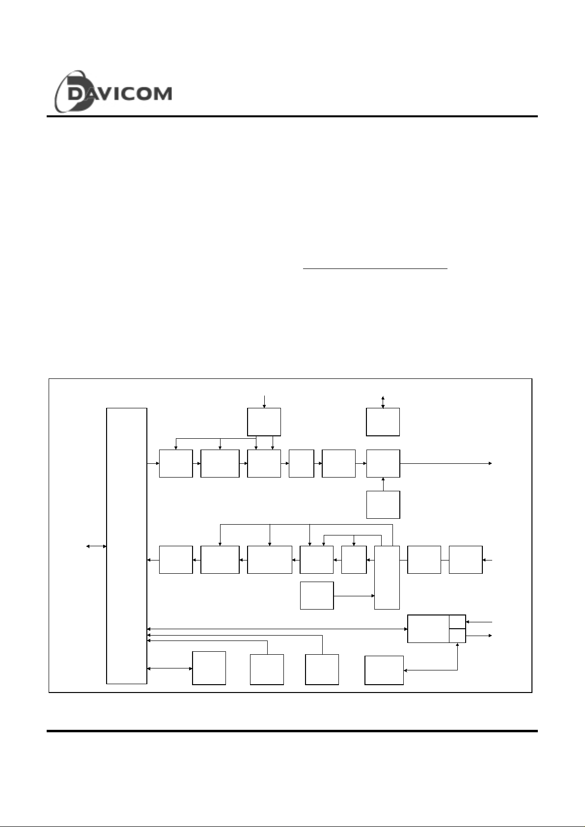
Block Diagram
TX CGM
Sublayer (PC S), Physi cal Me diu m A ttachmen t (PMA),
100Base-TX Twisted Pair Physical Medium Dependent
Sublayer (TP-PMD), and a 10Base-T Encoder/Decoder
(ENC/DEC). The DM9101 provides strong support for the
Auto-negotiation function utilizing automatic media speed
and protocol selection. The DM9101 incorporates an
internal wave-shaping filter to control rise/fall time,
el i m i n a t in g t h e need fo r e x t e rn al f i l te rin g o n the 10/100Mbps
signals.
Patent-Pending Circuitry Includes:
Smart adaptive receiver equalizer
Digital algorithm for high frequency clock/data recovery
circuit
High speed wave-shaping circuit
LED1-4#25M OSCI
LED
Driver
NRZ
to
NRZI
25M CLK
Serial to
Parallel
Digital
Logic
Carrier
Sense
NRZI to
MLT-3
125M CLK
NRZI
to
NRZ
MLT-3
Driver
Rise/Fall
Time
CTL
RX
CRM
Auto-
Negotiation
MLT-3 to
NRZI
10BASE-T
Module
Adaptive
EQ
RX
TX
100TXD+/-
RXI+/-
RXI+/10TXD+/-
MII
Signals
MII
Interface/
Control
4B/5B
Encoder
4B/5B
Decoder
Scrambler
Codegroup
Alignment
Register
Parallel
to Serial
Descrambler
Collision
Detection
Final 1
Version: DM9101 - DS -F03
July 22, 1999
Page 2

Table of Contents
DM9101
10/100Mbps Ethe rnet P hysical Layer Si ngle Chi p Transc ei ver
General Descri pti on................................................1
Block Diagram........................................................1
Features.................................................................3
Pin Configuration: DM9101E LQFP.........................3
Pin Configuration: DM9101F QFP...........................4
Pin Description .......................................................5
Functional Descr i pti on
MII Inter fa ce......................................................12
100Base-TX Operat ion......................................14
100Base-TX Transm it........................................14
100Base-TX Operat ion......................................15
4B5B Encoder ...................................................15
Scrambler..........................................................15
Paralle l to Serial Converter................................15
NRZ to NRZI Encoder........................................15
MLT-3 Converter ...............................................15
MLT-3 Driver .....................................................15
4B5B Code Group .............................................16
100Base-TX Receiver........................................17
Signal Detect.....................................................17
Digital Adaptive Equalization..............................17
MLT-3 to NRZI Decoder.....................................17
Clock Recovery Module.....................................18
NRZI to NRZ .....................................................18
Serial to Parallel................................................18
Descrambler......................................................18
Code Group Alignment ......................................18
4B5B Decoder...................................................18
10Base-T Operation..........................................18
Collisio n Detection.............................................18
Carrier Sense....................................................18
Auto-Negotiation................................................18
MII Serial Management......................................19
Serial Management Inter face.............................19
Management Interface – Read Frame Structure.19
Management Interface – Write Frame Structure.19
Register Description .............................................20
- Key To Default....................................................20
- Register 2 ..........................................................23
PHY ID Identifier Register #2 (PHYIDR2)
- Register 3 ..........................................................24
Auto-negotiation Advertisement Register (ANAR)
- Register 4 ..........................................................24
Auto-negotiation Link Partner Ability Register
(ANLPAR) - Register 5 .........................................25
Auto-negotiation Expansion Register (ANER)
- Register 6 ..........................................................26
DAVICOM Specified Configuration Register (DSCR)
- Register 16.........................................................26
DAVICOM Specified Configuration and Status
Register (DSCSR) - Register 17 ...........................28
10Base-T Configuration / Status (10BTS CRCS R)
- Register 18.........................................................29
Abso lu te Maximum Ratings..................................30
DC Electrical Characteristics ................................31
AC Characteristics................................................32
Timing Waveforms
MII-100Base-T X Tr ansmit Timing Diagram........33
MII-100Base-TX Receive Timing Diagram.........33
Auto-negotiation and Fast Link Pulse Timing.....34
MII-10Ba se-T Transmit Tim ing Diagram............35
MII-10Base-T Receive Nibble Timing Diagram ..35
10BASE-T SQE (Heartbeat) Timing Diagram.....36
10BASE-T Jab and Unjab Timing Diagram........36
MDIO Timing when OUTPUT by STA................37
MDIO Timing when OUTPUT by DM9101..........37
Magnetics Selection Guide...................................38
Crystal Selection Guide........................................38
Application Circuit (for reference only) ..................40
Basic Mode Control Register (BMCR)
- Register 0...........................................................21
Basic Mode Status Register (BMSR)
- Register 1...........................................................22
PHY ID Identifier Register #1 (PHYIDR1)
2 Final
Package Information.............................................41
Ordering Information.............................................42
Company Overview..............................................42
Contact Windows..................................................42
Version: DM9101 - DS -F03
July 22, 1999
Page 3

10/100Mbps Ethe rnet P hysical Layer Si ngle Chi p Transc ei ver
Features
• 10/100Base-TX physical-layer, single-chip transceiver
• Compliant with IEEE 802.3u 100Base-TX standard
• Compliant with ANSI X3T12 TP-PMD 1995 standard
• Compliant with IEEE 802.3u Auto-negotiation protocol
for a uto m at ic lin k typ e s e lec t ion
• Supports the MII with serial management interface
• Supports Full Duplex operation for 10 and 100Mbps
• High performance 100Mbps clock generator and data
recovery circuitry
• Adaptive equalization circuitry for 100Mbps receiver
Pin Configu ration: DM9101E LQFP
AGND
AGND
NC
AVCC
10BTSER
BPSCR
BP4B5B
BPALIGN
RPTR/NODE#
OPMODE3
OPMODE2
OPMODE1
OPMODE0
PHYAD4
DM9101
• Controlled output edge rates in 100Mbps
• Supports a 10Base-T interface without the need for
an external filter
• Provides Loop-back mode for system diagnostics
• Includes Flexible LED configuration capability
• Dig ita l clo c k r ec o ver y c irc u it us in g advance d digit al
algorithm to reduce jitter
• Low-power, high-performance CMOS process
• Available in both a 100 pin LQFP and a 100 QFP
package
PHYAD3
DGND
DVCC
PHYAD2
PHYAD1
PHYAD0
TESTMODE
RESET#
RX_ER/RXD4
RX_EN
RX_DV
NC
NC
NC
AGND
AVCC
AVCC
RXI-
RXI+
AGND
AGND
10TXO-
10TXO+
AVCC
AVCC
AGND
AGND
NC
NC
AVCC
AVCC
AGND
AGND
100TXO-
100TXO+
AVCC
11
18
1
2
4
7
8
9
10
12
13
14
15
16
17
19
20
21
22
23
24
25
8
99
98
97
100
3
5
6
96959493929190898887868584
DM9101E
26
27
3031323334353738394041
28
AVCC
OSCI/X1
29
X2
AGND
AVCC
AGND
BGREF
OSC/XTL#
36
DGND
DGND
BGRET
DVCC
DGND
UTP
TRIDRV
SPEED10
42
RX_LOCK
1
82
NC
LINKSTS
797877
80
DVCC
CLK25M
FDXLED#
COLLED#
83
43444546474849
DGND
76
75
74
73
72
71
70
69
68
67
66
65
64
63
62
6
1
60
59
58
57
56
55
54
53
52
5
1
50
DGND
COL
CRS
RX_CLK
DVCC
DGND
RXD0
RXD1
RXD2
RXD3
DVCC
DGND
MDIO
MDC
TX_CLK
TX_EN
DVCC
DGND
TXD0
TXD1
TXD2
TXD3
TX_ER/TXD4
TXLED#
RXLED#
LINKLED#
Final 3
Version: DM9101 - DS -F03
July 22, 1999
Page 4

Pin Configu ration: DM9101 F QFP
DM9101
10/100Mbps Ethe rnet P hysical Layer Si ngle Chi p Transc ei ver
AVCC
NC
NC
NC
NC
AGND
AVCC
RXI-
RXI+
AGND
AGND
10TXO-
10TXO+
AVCC
AVCC
AGND
AGND
NC
NC
AVCC
AVCC
AGND
AGND
100TXO-
100TXO+
AVCC
AVCC
OSCI/X1
X2
1
2
3
4
5
6
7
8
9
10
11
12
13
14
15
16
17
18
19
20
21
22
23
24
25
26
27
28
29
30
AGND
AGND
99
100
32
31
BP4B5B
BPSCR
10BTSER
96
97
98
35
34
33
OPMODE3
RPTR/NODE#
BPALIGN
93
94
95
OPMODE2
92
91
90
PHYAD4
89
OPMODE0
OPMODE1
DM9101F
36
37
38
39
424041
DVCC
PHYAD3
87
88
44
43
PHYAD2
DGND
85
86
46
45
PHYAD0
PHYAD1
83
84
48
47
RESET#
TESTMODE
81
82
80
79
78
77
76
75
74
73
72
71
70
69
68
67
66
65
64
63
62
61
60
59
58
57
56
55
54
53
52
51
50
49
RX_EN
RX_ER/RXD4
RX_DV
COL
CRS
RX_CLK
DVCC
DGND
RXD0
RXD1
RXD2
RXD3
DVCC
DGND
MDIO
MDC
TX_CLK
TX_EN
DVCC
DGND
TXD0
TXD1
TXD2
TXD3
TX_ER/TXD4
TXLED#
RXLED#
LINKLED#
DGND
COLLED#
AGND
OSC/XTL#
AVCC
AGND
BGRET
BGREF
DGND
DGND
DVCC
DGND
UTP
TRIDRV
SPEED10
NC
DGND
RX_LOCK
CLK25M
LINKSTS
DVCC
FDXLED#
4 Final
Version: DM9101 - DS -F03
July 22 , 1 999
Page 5

Pin Descr iption
Pin No. Pin Name I/O Description
LQFP QFP
MII Interface
54 56 TX_ER/
TXD4
DM9101
10/100Mbps Ethe rnet P hysical Layer Si ngle Chi p Transc ei ver
Transmit Error:
I
In 100Mbps mode, if this signal is asserted high and TX_EN is
active, the HALT sym bol is substituted for the actual data nibble.
In 10Mbps mode, this input is ignored.
In bypass modes (BP4B5B or BPALIGN), TX_ER becomes the
TXD4 pin, the fifth TXD data bit.
55-58 57 - 60 TXD3
TXD2
TXD1
TXD0
61 63 TX_EN I
62 64 TX_CLK O,Z
63 65 MDC I
64 66 MDIO I/O
67-70 69 - 72 RXD3
RXD2
RXD1
RXD0
73 75 RX_CLK O,Z
I
O,Z
Transmit Data:
Transmit data input pins for nibble data from the MII in 100Mbps
or 10Mbps nibble mode (25 MHz for 100Mbps mode, 2.5MHz for
10Mbps nibble mode) .
In 10Mbps serial mode, the TXD0 pin is used as the serial data
input pin. TXD[3:1] are ignored.
Transmit Enable:
Active high input indicates the presence of valid nibble data on
TXD[3:0] for both 100Mbps or 10Mbps nibbl e mode.
In 10Mbps serial mode, active high indicates the pres ence of
valid 10Mbps data on TXD0.
Transmit Clock:
Transmit c lock output from the DM9101:
- 25MHz nibble transmit clock derived from transmit Phase
Locked Loop(TX PLL) in 100Base-TX mode
- 2.5MHz transmit clock in 10Base-T nibble mode
- 10MHz transmit clock in 10Base-T serial mode
Management Data Clock:
Synchronous clock to the MDIO management data input/output
serial interface which is asynchronous to transmit and receive
clocks. The maximum clock rate is 2.5MHz.
Management Data I/O:
Bi-directional management instruction/data signal that may be
driven by the station management entity or the PHY. This pin
requires a 1.5KΩ pull-up resistor.
Receive Data:
Nibble wide receive data (synchronous to RX_CLK - 25MHz for
100Base-TX mode, 2.5MHz for 10Base-T nibble mode). Data is
driven on the falling edge of RX_CLK.
In 10Mbps serial mode, the RXD0 pin is used as the data output
pin. RXD[3:1] are ignored.
Receive Clock:
Provides the recover ed receiv e clock for diff er ent modes of
operation:
- 25MHz nibble clock in 100Mbps mode
- 2.5MHz nibble clock in 10Mbps nibble mode
- 10MHz receive clock in 10Mbps serial mode
Final 5
Version: DM9101 - DS -F03
July 22, 1999
Page 6

Pin Descr iption
Pin No. Pin Name I/O Description
LQFP QFP
MII Interface (continued)
74 76 CRS O,Z
75 77 COL O,Z
76 78 RX_DV O,Z
77 79 RX_ER/
78 80 RX_EN I
Media Interface
7, 8 9, 10 RXI-, RXI+ I
11, 12 13, 14 10 TXO-,
23, 24 25, 26 100 T XO - ,
(continued)
RXD4
10 TXO+
100 TXO+
O,Z
O
O
DM9101
10/100Mbps Ethe rnet P hysical Layer Si ngle Chi p Transc ei ver
Carrier Sense:
This pin is asserted high to indicate the presence of carrier due to
receive or transmit activities in 10Base-T or 100Base-TX Half
Duplex modes.
In Repeater, when Full Duplex or Loop-back mode is a logic 1, it
indicates the presence of carrier due only to receive a ctivity.
Collision Detect:
Asserted high to indicate detection of collision conditions in
10Mbps and 100Mbps Half Duplex modes. In 10Base-T Half
Duplex mode with Heart beat set active (bit 13, regi ster 18h) , it is
also asserted for a duration of approximately 1ms at the end of
transmission to indicate heartbeat. In F ull Duplex mode, this signal
is always logic 0. There is no heartbeat function in Full-Duplex
mode.
Receive Data Valid:
Asserted high to indicate that valid data is present on RXD[3:0].
Receive Error:
Asserted high to indicate that an invalid symbol has been detected
inside a received packet in 100Mbps mode.
In a bypass mode (BP4B5B or BPALIGN modes), RX_ER
becomes RXD4, the fifth RXD data bit of the 5B symbols.
Receive Enable:
Active high enabled for receive signals RXD[3:0], RX_CLK,
RX_DV and RX_ER. A low on this input tri-states these output
pins. For normal operation in a NODE application, this pin should
be pulled high.
100/10Mbps Differential Input Pair:
These pins are the differential receive input for 10Base-T and
100Base-TX. They are capable of receiving 100Base-TX MLT-3 or
10Base-T Manchester encoded data.
10Base-T Differential Output Pair:
This output pair provides controll ed rise and fall times designed to
filter the tr ansmitters output.
100Base-TX Differential Output Pair:
This output pair driv es MLT - 3 encoded data to the 100M twist ed
pair interface and provides controlled rise and fall times designed
to filter the transmitter output, reducing any associated EMI.
6 Final
Version: DM9101 - DS -F03
July 22, 1999
Page 7

DM9101
10/100Mbps Ethe rnet P hysical Layer Si ngle Chi p Transc ei ver
Pin Descr iption
Pin No. Pin Name I/O Description
LQFP QFP
LED Interface :
These outputs can dire c t ly drive LE Ds or provide status information to a network management device.
48 50 FDXLED#
49 51 COLLED# O
51 53 LINKLED#
52 54 RXLED# OD
53 55 TXLED# OD
Device Configuration/Control/Status Interface
40 42 UTP O
41 43 SPEED10 O
42 44 RX_LOCK O
45 47 LINKSTS O
(continued)
(POLLED)
(TRAFFIC
LED)
Polarity/Full Duplex LED:
O
Indicates Full Duplex mode status for 100Mbps and 10Mbps
operation (Active low). If bit 4 of Register 16 (FDXLED_MODE) i s
set, the FDXLED# pin function will change to indicate the Polarity
status for 10Mbps operation. If polarit y is inver ted, the POLLED
will go ON.
Collisi on LE D :
Indicates the presence of collision activit y fo r 10 Mbps and
100Mbps operation. This LED has no meaning for 10Mbps or
100Mbps Full Duplex operation (Active low).
Link LE D:
O
Indicates Good Link stat us for 10Mbps and 100Mbps operation
(Active low).
It functions as the TR A FFIC L ED when bit 5 of register 16 is set
to 1. In TRAFFIC LED mode, it is always ON when the link is OK.
The TRAFFIC LED flashes when transmitting or receiving.
Receive LED:
Indicates the presence of receive activity for 10Mbps and
100Mbps operation (Active low).
The DM9101 incorporates a "monostable" function on the RXLED
output. This ensures that even minimal r ec eiv e activity will
generate an adequate LED ON time.
Transmit LED:
Indicates the presence of transmit activity for 10Mbps and
100Mbps operation (Active low).
The DM9101 incorporates a "monostable" function on the TXLED
output. This ensures that even minimal transmit activity will
generate an adequate LED ON time.
UTP Cable Indication:
UTP=1: Indicates UTP cable is used.
Speed 10Mbps:
When set high, this bit indicates a 10Mbps operation, when set
low 100Mbps operati on. This pin can drive a low current LED to
indicate that 100Mbps operation is selected.
Lock for Clock/Data Recovery PLL:
When this pin is high i t indicates that the receiver recovery PLL
logic has locked to the input data stream.
Link Status Register Bit:
This pin reflects the status of bit 2 register 1.
Final 7
Version: DM9101 - DS -F03
July 22, 1999
Page 8

10/100Mbps Ethe rnet P hysical Layer Si ngle Chi p Transc ei ver
Pin Descr iption
Pin No. Pin Name I/O Description
LQFP QFP
Device Configuration/Control/Status Interface (continued)
88-91 90 - 93 OPMODE0
(continued)
OPMODE1
OPMODE2
OPMODE3
OPMODE0 - OPMODE3:
I
These pins are used to control the forced o r advertised operating
mode of the DM9101 (see table below). The value is latched into
the DM9101 registers at power-up/reset.
OPMODE3 OPMODE2 OPMODE1 OPMODE0 Function
0 0 0 0 Auto-neg enable
0 0 0 1 Auto-neg enable
0010Auto-neg 100TX
0011Auto-neg 100TX
0 1 0 0 Auto-neg 10TP
0 1 0 1 Auto-neg 10TX
0 1 1 0 Manual select
0 1 1 1 Manual select
1 0 0 0 Manual select
1 0 0 1 Manual select
DM9101
with all
capabilities with
Flow Control
without all
capabilities
without Flow
Control
FDX with Flow
Control onl y
FDX/HDX
without Flow
Control
FDX with Flow
Control onl y
FDX/HDX
without Flow
Control
100TX FD X
100TX HD X
10TX FDX
10TX HDX
92 94 RTPR/NOD
E#
Repeater/Node Mode:
I
When set high, this bit selects REPEATER mode; when set low, it
selects NODE. In REPEATER mode or NODE mode with Full
Duplex configured, the Carrier Sense (CRS) output from the
DM9101 will be asserted only during receive activity. In NODE
mode or a mode not configured for Full Duplex operation, CRS will
be asserted during receive or transmit activity. At power-up/reset,
the value on this pin is latched into Register 16, bit 11.
93 95 BPALIGN I
Bypass Alignment:
Allows 100Mbps transmit and receive data streams to bypass all
of the transmit and receive operations when set high.
At power-up/reset, the value on this pin is latched into bit Register
16 ,bit 13.
8 Final
Version: DM9101 - DS -F03
July 22, 1999
Page 9

10/100Mbps Ethe rnet P hysical Layer Si ngle Chi p Transc ei ver
Pin Descr iption
Pin No. Pin Name I/O Description
LQFP QFP
Device Configuration/Control/Status Interface (continued)
94 96 BP4B5B I
95 97 BPSCR I
96 98 10BTSER I
(continued)
Bypass 4B5B Encoder/Decoder:
Allows 100Mbps transmit and receive data streams to bypass the
4B to 5B encoder and 5B to 4B decoder circuits when set high
At power-up/reset, the value on this pin is latched into Register
16, bit 15.
Bypass Scrambler/Descrambler:
Allows 100Mbps transmit and receive data streams to bypass the
scrambler and descrambler circuits when set high.
At power-up/reset, the value on this pin is latched into Register
16, bit 14.
Serial/Nibble Select:
10Mbps Serial Operation:
When set high, this input selec ts a serial data transfer mode.
Manchester encoded transmit and receive data is exchanged
serially with a 10MHz clock rate on the least significant bits of the
nibble-wide MII data buses, pin TXD[0] and RXD[0] respectively.
This mode is intended for use with the DM9101 connected to a
device (MAC or Repeater) that has a 10Mbps serial interface.
Serial operation is not supported in 100Mbps mode. For
100Mbps, this input is ignored.
DM9101
Clock Interface
27 29 OSCI/X1 I
28 30 X2 O
30 32 OSC/XTL# I
46 48 CLK25M O,Z
10 and 100Mbps Nibble Operation:
When set low, this input selects the MII c om pliant nibble data
transfer mode. Transmit and receive data is exchanged in nibbles
on the TXD[3:0] and RXD[3:0] pins respectively.
At power-up/reset, the value on this pin is latched into Register
18, bit 10.
Cryst al or Oscillator Input:
This pin should be connected to a 25MHz (±50 ppm) crystal if
OSC/XTL#=0 or a 25MHz (±50ppm) external TTL oscillator input,
if OSC/XTLB=1.
Crystal Oscillat or Output:
An external 25MHz (±50 ppm) crystal should be connected to th is
pin if OSC/XTL#=0, or left unconnected if OSC/XTL#=1.
Cryst al or Oscillator Selec t or Pin:
OSC/XTL#=0: An external 25MHz (±50ppm) crystal should be
connected to X1 and X2 pins.
OSC/XTL#=1: An external 25MHz (±50ppm) oscillator should be
connected to X1 and X2 should be left
unconnected.
25MHz Clock Output:. This clock is derived directly from the
crystal circuit.
Final 9
Version: DM9101 - DS -F03
July 22, 1999
Page 10

DM9101
10/100Mbps Ethe rnet P hysical Layer Si ngle Chi p Transc ei ver
Pin Descr iption
Pin No. Pin Name I/O Description
LQFP QFP
PHY Address Interface:
PHYAD[4:0] provides up to 32 unique PHY address. An address selection of all zeros (00000) will result in a
PHY isolation condition. See the isolate bit description in the BMCR, address 00.
81 83 PHYAD0 I
82 84 PHYAD1 I
83 85 PHYAD2 I
86 88 PHYAD3 I
87 89 PHYAD4 I
Miscellaneous
1-3,
17, 18,
44,
100
33 35 BGREF I
34 36 BGRET I
39 41 TRIDRV I
79 81 RESET# I
80 82 TESTMODE I
2 - 5,
19, 20,
46
(continued)
NC
PHY Address 0:
PHY address bit 0 for mult iple PH Y address applications. The
status of this pin is latched into Register 17, bit 8 duri ng power
up/reset.
PHY Address 1:
PHY address bit 1 for mult iple PH Y address applications. The
status of this pin is latched into Register 17, bit 7 duri ng power
up/reset.
PHY Address 2:
PHY address bit 2 for mult iple PH Y address applications. The
status of this pin is latched into Register 17, bit 6 duri ng power
up/reset.
PHY Address 3:
PHY address bit 3 for mult iple PH Y address applications. The
status of this pin is latched into Register 17, bit 5 duri ng power
up/reset.
PHY Address 4:
PHY address bit 4 for mult iple PH Y address applications. The
status of this pin is latched into Register 17, bit 4 duri ng power
up/reset.
No Connect:
Leave these pins unconnected (floating).
Bandgap Voltage Reference:
Connect a 6.01KΩ, 1% resistor between this pin and the BGRET
pin to provide an accurate current reference for the DM9101.
Bandga p Voltage Reference Retur n:
Return pin for 6.01KΩ resistor connection.
Tri-state Digital Output Pins:
When set high, all digital output pins are set to a high impedance
state, and I/O pins, go to input mode.
Reset: Active Low input that initializes the DM9101. It should
remain low for 30ms after VCC has stabilized at 5Vdc (normal)
before it transitions high.
Test Mode Control Pin:
TESTMODE=0: Normal operating mode.
TESTMODE=1: Enable test mode.
10 Final
Version: DM9101 - DS -F03
July 22, 1999
Page 11

DM9101
10/100Mbps Ethe rnet P hysical Layer Si ngle Chi p Transc ei ver
Pin Descr iption
Power a nd Ground Pins :
The power (VCC) and ground (GND) pins of the DM9101 are grouped in pairs of two categories - Digital
Circuitry Power/Ground Pairs and Analog Circuitry Power/Ground Pair.
Pin No. Pin Name I/O Description
LQFP QFP
Group A - Digital Supply Pairs
35, 36,
37, 43,
50, 59,
65, 71,
84
Group A - Digital Supply Pairs (continued)
38, 47,
60, 72,
66, 85
Group B - Analog Circuit Supply Pairs
4, 9,
10, 15,
16, 21,
22, 29,
32, 97,
98
5, 6,
13, 14,
19, 20,
25, 26,
31, 99
6, 11, 12,
27, 28, 33
37, 38,
39, 45,
52, 61,
67, 73,
86
40, 49,
62, 74,
68, 87
18, 17,
23, 24,
31, 34,
99, 100
1, 7, 8,
15, 16,
21, 22,
(continued)
DGND P Digital Logic Ground.
DVCC P Digital Logic power supply
AGND P Analog circuit ground
AVCC P Analog circuit power supply
Final 11
Version: DM9101 - DS -F03
July 22, 1999
Page 12

DM9101
10/100Mbps Ethe rnet P hysical Layer Si ngle Chi p Transc ei ver
Functional D escrip tion
The DM9101 Fast Ethernet single-chip transceiver,
provides the functionality as specified in IEEE 802.3u,
integrates a complete 100Base-TX module and a
complete 10Base-T module. The DM9101 provides a
Media Independent Interface (MII) as defined in the IEEE
802.3u standard (Clause 22).
MII Interface
Carrier
Sense
The DM9101 performs all PCS (Physical Coding
Sublayer), PMA (Physical Media Access), TP-PMD
(Twisted Pair Physical Medium Dependent) sublayer,
10Base-T Encoder/Decoder, and Twisted Pair Media
Access Unit (TPMAU) functions. Figure 1 show s the major
functional blocks implemented in the DM9101.
100Base-TX
Transmitter
100Base-TX
Receiver
10Base-T
Tranceiver
Collision
Detection
Auto
Negotiation
MII Serial
Management
Interface
MII Interface
The DM 9101 provides a Media Independent Int erfa ce (M II)
as defined in the IEEE 802.3u standard (Clause 22).
The purpose of the MII interface is to provide a simple, easy
to implement connection between the MAC Reconcilia tio n
layer and the PHY. The MII is designed to make the
differences between various media transparent to the MAC
sublayer.
The MII consists of a nibble wide receive data bus, a n ibble
wide transmit data bus, and control signals to facilitate d ata
transfers between the PHY and the Reconciliation layer.
Figure 1
• TXD (transmit data) is a nibble (4 bits) of da ta that are
driven by the reconciliation sublayer synchronously with
respect to TX_CLK. For each TX_CLK period which
TX_EN is asserted, TXD (3:0) are accepted for
transmission by the PHY.
• TX_CLK (transmit clock) output to the MAC
reconciliation sublayer is a continuous clock that
provides the timing reference for the transfer of the
TX_EN, TXD, and TX_ER signals.
• TX_EN (transmit enable) input from the MAC
reconciliation sublayer to indicate nibbles are being
presented on the MII for transmission on the physical
medium.
12 Final
Version: DM9101 - DS -F03
July 22, 1999
Page 13
DM9101
10/100Mbps Ethe rnet P hysical Layer Si ngle Chi p Transc ei ver
• MII Interface (continued)
• TX_ER (transmit coding error) transitions
synchronously with respect to TX_CLK. If TX_ER is
asserted for one or more clock peri ods, and TX_EN is
asserted, the PHY will emit one or more symbols that
are not part of the valid data delimiter set somewhere in
the frame being transmitted.
• RXD (receive data) is a nibble (4 b its) of data that are
sampled by the reconciliation sublayer synchronously
with respect to RX_CLK. For each RX_CLK period
which RX_DV is asserted, RXD (3:0) are trans ferred
from the PHY to the MAC reconciliation s ublayer.
• RX_CLK (receive clock) output to the MAC
reconciliation sublayer is a continuous clock that
provides the timing reference for the transfer of the
RX_DV, RXD, and RX_ER signals.
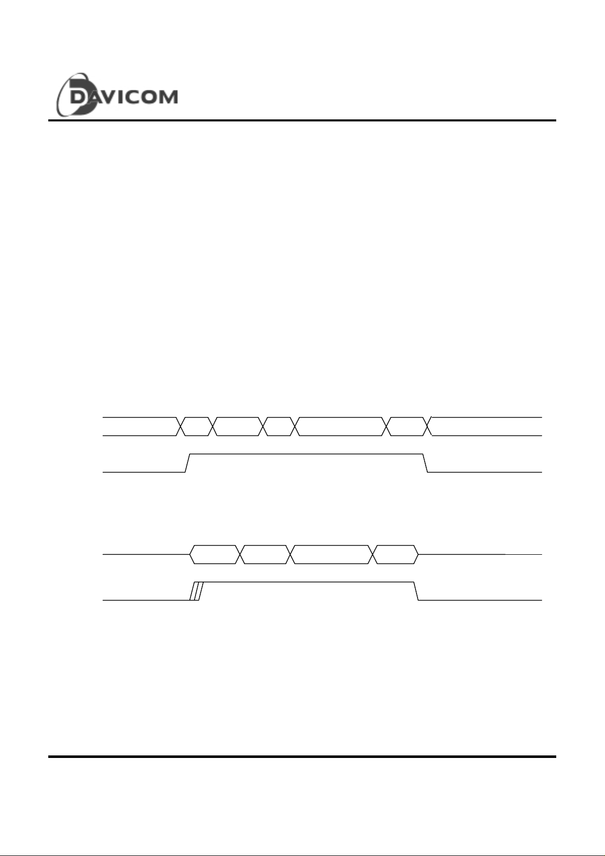
TXD
IDLE
SSD
J/K
Preamble
SFD
• RX_DV (receive data v alid) input from the PHY to
indicate the PHY is presenting recovered and decoded
nibbles to the MAC reconciliation sublayer. To interpret
a receive frame correctly by the reconciliation sublayer,
RX_DV must encompass the frame starting no later
than the Start-of-Frame delimiter and excluding any
End-Stream delimiter.
• RX_ER (receive error) transiti ons synchronously with
respect to RX_CLK. RX_ER will be asserted for 1 or
more clock periods to indicate to the reconciliation
sublayer that an error was detected somewhere in the
frame being transmitted from the PHY to the
reconciliation sublayer.
• CRS (carrier sense) is asserted by the PHY when
either the transmit or receive medium is non-idle and
deasserted by the PHY when the transmit and rece ive
mediu m are id le. Figure 2 d epi cts the beha vior of CRS
during 10Base-T and 100Base-TX transmission.
Data
ESD
T/R
IDLE
CRS
TXD
CRS
Preamble SF D
100Base-TX
10Base-T
Figure 2
Data
EFD
Final 13
Version: DM9101 - DS -F03
July 22, 1999
Page 14

DM9101
10/100Mbps Ethe rnet P hysical Layer Si ngle Chi p Transc ei ver
100Base-TX Operation
The 100Base-TX tran smitter receives 4-bit nibble data
clocked in at 25MHz at the MII, and o utputs a sc rambled
5-bit encoded MLT-3 signal to the media a t 100Mbps. The
on-chip clock circuit converts the 25MHz clock into a
125MHz clock for internal us e.
The IEEE 802.3u specification defines the Media
Independent Interface. The interface specification defines
a dedic ated rec eive data bus and a dedicated transmit
data bus.
TX CGM
TXCLK
TXEN
TXER
Transmit
MII
Interface/
Control
4B/5B
Encoder
Scrambler
Parallel
to Serial
These two busses include va rious c ontr ols and signal
indications that facilitate data tr a nsfers between the
DM9101 and the Reconciliation layer.
100Base-TX Transmit
The 100Base-TX tran smitter consists of the functional
blocks shown in figure 3. The 100Base-TX transmit
section converts 4-bit synchronous data provided by the
MII to a scrambled MLT-3 125 million symbols per second
serial data stream.
LED1-4#25M OSCI
LED
Driver
NRZ
to
NRZI
NRZI to
MLT-3
MLT-3
Driver
Rise/Fall
Time
CTL
10BASE-T
Module
RX
TX
100TXD+/-
RXI+/-
10TXD+/-
TXD (3:0
Register
Collision
Detection
Carrier
Sense
Figure 3
14 Final
Version: DM9101 - DS -F03
July 22, 1999
Page 15

10/100Mbps Ethe rnet P hysical Layer Si ngle Chi p Transc ei ver
100Base-TX Operation
The block diagram in figure 3 provides an overview of the
functional blocks contained in the transmit s ection.
The transmitter section contains the following functional
blocks:
- 4B5B Encoder
- Scrambler
- Parallel to Serial Converter
- NRZ to NRZI Con verter
- NRZI to MLT-3
- MLT-3 D river
DM9101
By scra mbl ing the data, the to tal energy presented to the
cable is randomly distributed over a wide frequency range.
Without the scrambler, energy levels on the cable could
peak beyond FCC limitations at frequencies related to
repeated 5B sequences like continuous transmission of
IDLE symbols. The scrambler output is combined with the
NRZ 5B data from the code-group encoder via an XOR
logic function. The result is a scrambled data stream with
sufficient randomization to decrease radiated emissions at
critical frequencies.
Parallel to Serial Converter
4B5B Encoder
The 4B5B encoder converts 4-bit (4B) nibble data
generated by the MAC Reconciliation Layer into a 5-bit
(5B) code group for transmission, reference Table 1. This
conversion is required for control and packet data to be
combined in code groups. The 4B5B encoder substitutes
the first 8 bits of the MAC preamble with a J/K code-group
pair (11000 10001) upon transmit. The 4B5B encoder
continues to replace subsequent 4B preamble and data
nibbles with corresponding 5B code-groups. At the end of
the transmit packet, upon the deassertion of the Transmit
Enable signal from the MAC Reconciliation layer, the
4B5B encoder injects the T/R code-group pair (01101
00111) indicating end of fr ame. After the T/R code-group
pair, the 4B5B encoder continuously injects IDL Es i nto the
transmit data stream until Transmit Enable is asserted and
the next transmit packet is detected.
The DM9101 includes a Bypass 4B5B conversion option
within the 100Base-TX Transmit te r for support of
applications like 100 Mbps repeaters which do not require
4B5B conversion.
Scrambler
The scrambler is required to control the radiated emissions
(EMI) by spreading the transmit energy across the
frequency spectrum at the media connector and on the
twisted pair cable in 100Base-TX operation.
The Parallel to Serial Converter receives parallel 5B
scrambled data from the scrambler and serializes it
(converts it f r om a parallel to a serial dat a stream).
The serialized data stream is then presented to the
NRZ to NRZI Encoder block
NRZ to NRZI Encoder
After the transmit data stream has been scrambled and
serialized, the data must be NRZI encoded for
compatibility with the TP-PMD standard for 100Base-TX
transmission over Category-5 unshielded twisted pair
cable.
MLT-3 Converter
The MLT-3 conversion is accomplished by converting
the dat a stre am o utput from the NR ZI en coder into two
binary data streams with alternately phased logic one
events.
MLT-3 Driver
The two binary data streams created at the MLT-3
converter are fed to the twisted pair output driver which
converts these streams to current sources and alternately
drives either side of the transmit transforme r primary
winding resulting in a minimal current MLT-3 signal. Refer
to figure 4 for the block diagram of the MLT-3 converter.
Final 15
Version: DM9101 - DS -F03
July 22, 1999
Page 16

4B5B Code Group
DM9101
10/100Mbps Ethe rnet P hysical Layer Si ngle Chi p Transc ei ver
Symbol Meaning 4B code
3210
0 Data 0 0000 11110
1 Data 1 0001 01001
2 Data 2 0010 10100
3 Data 3 0011 10101
4 Data 4 0100 01010
5 Data 5 0101 01011
6 Data 6 0110 01110
7 Data 7 0111 01111
8 Data 8 1000 10010
9 Data 9 1001 10011
A Data A 1010 10110
B Data B 1011 10111
C Data C 1100 11010
D Data D 1101 11011
E Data E 1110 11100
F Data F 1111 11101
I Idle undefined 11111
J SFD (1) 0101 11000
K SFD (2) 0101 10001
T ESD (1) undefined 01101
R ESD (2) undefined 00111
H Error undefined 00100
5B Code
43210
V Invalid undefined 00000
V Invalid undefined 00001
V Invalid undefined 00010
V Invalid undefined 00011
V Invalid undefined 00101
V Invalid undefined 00110
V Invalid undefined 01000
V Invalid undefined 01100
V Invalid undefined 10000
V Invalid undefined 11001
Table 1
16 Final
Version: DM9101 - DS -F03
July 22, 1999
Page 17

DM9101
10/100Mbps Ethe rnet P hysical Layer Si ngle Chi p Transc ei ver
D
Q
.
Q
CK
Binary In
.
Binary In
MLT-3
100Base-TX Receiver
The 100Base-TX receiver contains s everal function blocks
that convert the scrambled 125Mb/s serial data to
synchronous 4-bit nibble data that is then provided to the
MII.
The receive section contains the following functional
blocks:
- Signal Detect
- Digital Adaptive Equalization
- MLT-3 to Binary Decoder
- Clock Recovery Module
- NRZI to NRZ D ecoder
- Serial to Pa ralle l
- Descra mbler
- Code Group Alignment
- 4B5B Decoder
Signal Detect
The signal detect function meets the specifications
mandated by the ANSI XT12 TP-PMD 100Base-TX
Standards for both voltage thresholds and timing
parameters.
Binary plus
Binary minus
Figure 4
Common
driver
MLT-3
Digital Adaptive Equalization
When transmitting data at high speeds over copper
twisted pair cable, attenuation based on frequency
becomes a concern. In high speed twisted pair signaling,
the frequency content of the tran smitt e d signal can vary
greatly during normal operation based on the randomness
of th e s cr a mbled data stream. This vari a tion i n signal
attenuation caused by frequency variations must be
compensated for to ensure the integrity of the received
data. In order to ensure quality transmission when
employing MLT-3 encoding, the compensation must be
able to adapt to various cable lengths and cable types
depending on the installed environment. The selection of
long cable lengths for a given implementation, requires
significant compensation which will be over-kill in a
situation that includes shorter, less attenuating cable
lengths. Conversely, the selection of short or intermediate
cable lengths requiring less compensation will cause
serious under-compensation for longer length cables.
Therefore, the compensation or equali zat ion m u st be
adaptive to ensure proper co nditi oni n g of the re cei v ed
signal independent of the cable length.
MLT-3 to NRZI Decoder
The DM9101 decodes the MLT-3 information from the
Digital Adaptive Equalizer into NRZI data. The re lationship
between NRZI and MLT-3 data is shown in figure 4.
Final 17
Version: DM9101 - DS -F03
July 22, 1999
Page 18

DM9101
10/100Mbps Ethe rnet P hysical Layer Si ngle Chi p Transc ei ver
Clock Recovery Module
The Clock Recovery Module accepts NRZI data from the
MLT-3 to NRZI decoder. The Clock Recovery Module
locks onto the data stream and extracts the 125Mhz
reference clock. The extracted and synchronized clock
and data are presented to the NRZI to NRZ Decoder.
NRZI to NRZ
The transmit data stream is required to be NRZI encoded
in for compatibility with the TP-PMD standard for
100Base-TX transmission over Category-5 unshielded
twisted pair cable. This conversion process must be
reversed on the receive end. The NRZI to NRZ
decoder, receives the NRZI data stream from the
Clock Recovery Module and converts it to a NRZ
data stream to be presented to the Serial to Parallel
conversion block.
Serial to Para llel
The Serial to Parallel Converter receives a serial
data stream from the NRZI to NRZ converter, and
converts the data stream to parallel data to be
presented to the descrambler.
Descrambler
The T/R symbol pair is also stripped from the nibble
presented to the Reconciliation layer.
10Base-T Operation
The 10Base-T transceiver is IEEE 802.3u compliant.
When the DM9101 is operating in 10Base-T mode, the
coding scheme is Manchester. Data processed for
transmit is presented to the MII interface in n ibble format,
converted to a serial bit stream, then Manchester
encoded. When receiving, the Manchester encoded bit
stream is decoded and converted into nibble form at for
presentation to the MII interface.
Collis ion D ete c ti on
For half-duplex operation, a collision is detected when the
transmit and receive channels are active simultaneously.
When a collision has been detected, it will be reported by
the C OL sig na l on the MI I inte r face . Co ll is ion d et ection i s
disabled in Full Duplex operation.
Carrier Sense
Carrier Sense (CRS) is asserted in half-duplex operation
during transmission or reception of data. During full-duplex
mode, CRS is asserted only during receive operations.
Because of the scrambling process required to control the
radiated emissions of transmit data streams, the receiver
must descramble the receive data streams. The
descrambler receives scrambled parallel data streams
from the Serial to Parallel converter, descrambles the data
streams, and presents the data streams to the Code
Group alignment block.
Code Gro up Alignment
The Code Group Alignment block receives unaligned 5B data from the descrambler and con ver ts
it into 5B code group data. Code Group Alignment
occurs after t he J/K is detected, and subseq uent
data is aligned on a fixed boundary.
4B5B Decoder
The 4B5B Decoder functions as a look-up table that
translates incoming 5B code groups into 4B (Nibble) data.
When receiving a frame, the first 2 5-bit code groups
received are the start-of-frame delimiter (J/K symbols).
The J/K symbol pair is stripped and two nibbles of
preamble pattern are substituted. The last two code
groups are the end-of-frame delimiter (T/R symbols).
18 Final
Auto-Negotia tion
The objective of Auto-negotiation is to pr ov i d e a means to
exchange information between segment linked devices
and to automatically configure both devices to take
maximum advantage of their abilities. It is important to note
that Auto-negotiation does not test the li nk se gment
characteristics. The Auto-Negotiation function provides a
means for a device to advertise supported modes of
operation to a remote link partner, acknowledge the
receipt and understanding of common modes of
operation, and to reject un-shared modes of operation.
This allows devices on both ends of a segment to
establish a link at the best common mode of opera tion. If
more than one common mode exists between the two
devices, a mechanism is provided to allow the devices to
resolve to a single mode of operation using a
predetermined priority resolution function.
Version: DM9101 - DS -F03
July 22, 1999
Page 19

10/100Mbps Ethe rnet P hysical Layer Si ngle Chi p Transc ei ver
Auto-Negotia tion (continued)
Auto-negotiation also provides a parallel detection
function for devices that do not support the Autonegotiation feature. During Parallel detection there
is no exchange of configuration information,
instead, the receive signal is examined. If it i s
discovered that the signal matches a technology
that the receiving device supports, a connection will
be automatically established using that technology.
This allows devices that do not support Autonegotiation but support a common mode of
operation to establish a link.
DM9101
In read/write operation, the management data frame
is 64-bits l ong and starts with 32 contiguous lo gi c
one bits (preamble) synchronization clock cycles on
MDC. The Start of Fram e Delimiter (SFD) is
indicated by a <01> pattern followed by the
operation code (OP):<10> indicates Read operation
and <01> indicates Write operation. For read
operation, a 2-bit turnaround (TA) filin g between
Register Address field and Data field is provided for
MDIO to avoid contention. Following the turnaround
time, 16-bit data is read from or written onto
management regi ster s.
MII Ser ia l Management
The MII serial management interface consists of a
data interface, basic register set, and a serial
management interface to the register set. Through
this interface it is possible to control and configure
multiple PHY devices, get status and error
information, and determine the type and capabilities
of the attached PHY device(s).
The DM9101 management functions correspond to
MII specification for IEEE 802.3u-1995 (Clause 22)
for registers 0 through 6 with vendor-specific
registers 16,17, and 18.
Management Interface - Read Frame Structure
MDC
MDIO Read
32 "1"s
Idle Preamble SFD Op Code PHY Address Register Address Turn Around Data Idle
0110A4A3A0R4R3R0
Write
Management Interface - Write Frame Structure
Serial Management Interface
The serial control interface uses a simple two-wired
serial interface to obtain and control the status of
the physical layer through the MII interface. The
serial control interface consists of MDC
(Management Data Clock), and MDI/O
(Management Data I nput/Output) signals.
The MDIO pin is bi-directional and may be shared
by up to 32 devices.
0
Z
D15 D14 D1 D0
//
Read
//
MDC
MDIO Write
32 "1"s 0 1 10 A4 A3 A0 R4 R3 R0 1 0 D15 D14 D1 D0
Idle Preamble SFD Op Code PHY Address Register Address Turn Around Data Idle
Write
Figure 5
Final 19
Version: DM9101 - DS -F03
July 22, 1999
Page 20

10/100Mbps Ethe rnet P hysical Layer Si ngle Chi p Transc ei ver
Register Description
Register Address Register Name Description
0 BMCR Basic Mode Control Register
1 BMSR Basic Mode Status Register
2 PHYIDR1 PHY Identifier Register #1
3 PHYIDR2 PHY Identifier Register #2
4 ANAR Auto-Negotiation Advertisement Register
5 ANLPAR Auto-Negotiation Link Partner Ability Register
6 ANER Auto-Negotiation Expansion Register
16 DSCR DAVICOM Specified Configuration Register
17 DSCSR DAVICOM Specified Configuration/Status Register
18 10BTCSR 10Base-T Configur ation/Status Register
Others Reserved Reserved For Future Use-Do Not Read/Write To These Registers
Key to Default
In the register description that follows, the default column takes the form:
<Reset Value>, <Access Type> / <Attribute(s)>
Where
<Reset Value>:
DM9101
1 Bit set to logic one
0 Bit set to logic zero
X No default value
(PIN#) Value latched in from pin # at reset
<Access Type>:
RO = Read onl y
RW = Read/Write
<Attribute (s)>:
SC = Self clearing
P = Value permanently set
LL = Latching low
LH = Latching high
20 Final
Version: DM9101 - DS -F03
July 22, 1999
Page 21

10/100Mbps Ethe rnet P hysical Layer Si ngle Chi p Transc ei ver
Basic Mode Control Register (BMCR) - Register 0
Bit Bit Name Default Description
0.15 Reset 0, RW/SC
0.14 Loopback 0, RW
0.13 Speed Selection 1, RW
0.12 Auto-negotiation
Enable
0.11 Power Down 0, RW
0.10 Isolate (PHYAD=
1, RW
00000),
RW
Reset:
1=Software res e t
0=Normal operation
When set this bit c onfigures the PHY status and control
registers to thei r default states. This bit will return a value of
one until the reset process i s complete
Loopback:
Loopback control register
1=Loopback enabled
0=Normal operation
When in 100M operati on is selected, setting this bit will cause
the descrambler to lose synchronization. A 720ms "dead time"
will occur before any valid data appears at the MII receive
outputs
Speed Select:
1=100Mbps
0=10Mbps
Link speed may be selected either by this bit or by Autonegotiation if bit 12 of this register is set. When Autonegotiation is enabled, this bit will return Auto-negotiation link
speed.
Auto-negotiation En able:
1= Auto-negoti ati on enabled:
0= Auto-negoti ati on disabled:
When auto-negotiation is enabled bits 8 and 13 will contain the
Auto-negotiation results. When Auto-negotiation is disabled bits
8 and 13 will determine the duple x m od e and link speed
Power Down:
1=Power Down
0=Normal Operation
Setting this bit will power down the DM9101 with the exception
of the crystal oscill ator circuit
Isolate:
1= Isolate
0= Normal Operation
When this bit is set the data path will be isolated from the
MII interface. TX_CLK, RX_CLK, RX_DV, RX_ER,
RXD[3:0], COL and CRS will be placed in a high impedance
state. The management interface is not effected by this bit.
When the PHY Address is set to 00000 the isolate bit will be
set upon power-up/reset
DM9101
Final 21
Version: DM9101 - DS -F03
July 22, 1999
Page 22

10/100Mbps Ethe rnet P hysical Layer Si ngle Chi p Transc ei ver
Basic Mode Control Register (BMCR) - Register 0 (continued)
Bit Bit Name Default Description
0.9 Restart Autonegotiation
0.8 Duplex Mode 1,RW
0.7 Collision Test 0,RW
0.6 Reserved 0,RO
0,RW/SC
Restart Auto-negotiation:
1= Restart Auto-negot iation.
0= Normal Operation
When this bit is set the Auto-negot iation process is re-initiated.
When Auto-negoti ation is disabled (bit 12 of this register
cleared), this bit has no function and it should be cleared. This
bi t is s elf-clearing and will return a value of 1 until Autonegotiation is initiated. The operation of the Auto-negotiation
process will not be affected by the management entity that
clears thi s bit
Duplex Mode:
1= Full Duplex operation.
0= Normal operation
If Auto-negotiation is disabled, setting this bit will cause the
DM9101 to operate in full duplex mode. When Auto-negotiation
is enabled, thi s bit r eflects the duple x selected by Autonegotiation
Collisi on Te s t :
1= Collision Test enabl ed.
0= Normal Operation
When set, this bit will cause the COL signal to be asserted in
response to the assertion of TX_EN
Reserved:
Write as 0, ignore on read
DM9101
Basic Mode Status Register (BMSR) - Register 1
Bit Bit Name Default Description
1.15 100Base-T4 0,RO/P
1.14 100Base-TX
Full Duplex
1.13 100Base-TX
Half Duplex
1.12 10Base-T
Full Duplex
1.11 10Base-T
Half Duplex
1.10-1.7 Reserved 0,RO
1,RO/P
1,RO/P
1,RO/P
1,RO/P
100Base-T4 Capable:
1=DM9101 is able to perform in 100Base-T4 mode
0=DM9101 is not able to perform in 100Base-T4 mode
100Base-TX Full Duplex Capable:
1= DM9101 is able to perform 100Base-TX in Full Duplex mode
0= DM9101 is not able to perform 100Base-TX in Full Duplex
mode
100Base-TX Half Duplex Capable:
1=DM9101 is able to perform 100Base-TX in Half Duplex mode
0=DM9101 is not able to perform 100Base-TX in Half Duplex
mode
10Base-T Full Duplex Capable:
1=DM9101 is able to perform 10Base-T in Full Duplex mode
0=DM9101 is not able to perform 10Base-T in Ful l Du plex
mode
10Base-T Half Dupl ex Capable:
1=DM9101 is able to perform 10Base-T in Half Duplex mode
0=DM9101 is not able to perform 10Base-T in Half Duplex
mode.
Reserved:
Write as 0, ignore on read
22 Final
Version: DM9101 - DS -F03
July 22, 1999
Page 23

10/100Mbps Ethe rnet P hysical Layer Si ngle Chi p Transc ei ver
Basic Mode Status Register (BMSR) - Register 1 (continued)
Bit Bit Name Default Description
1.6 MF Preamble
Suppression
1.5 Auto-negotiation
Complete
1.4 Remote Fault 0,
1.3 Auto-negotiation
Ability
1.2 Link Status 0,RO/LL
1.1 Jabber Detect 0,
1.0 Extended
Capability
0,RO
0,RO
RO/LH
1,RO/P
RO/LH
1,RO/P
MII Frame Preamble Suppression:
1=PHY will accept management frames with preamble suppressed
0=PHY will not accept management frames with preamble suppressed
Auto-negotiat ion Com plete:
1=Auto-negotiation process completed
0=Auto-negotiation process not completed
Remote Fault:
1= Remote fault condition detected (cleared on read or by a chip reset).
Fault criteria and dete ction method is D M9101 implementation specific.
This bit will set after the RF bit in the ANLPAR (bit 13, register address
05) is set
0= No remote fault condition detected
Auto C onf igur at io n A bil ity:
1=DM9101 able to perform Auto-negotiation
0=DM9101 not able to perform Auto-negotiation
Link S tatus :
1=Valid link established (for either 10Mbps or 100Mbps operation)
0=Link not established
The link status bit is implemented with a latching function, so that the
occurrence of a link failure condition causes the Link Status bit to be
cleared and remain cleared until it is read via t h e management interface
Jabber Detect:
1=Jabber condition detected
0=No jabber condition detected
This bit is implemented with a latching function. Once Jabber conditions
are detected thi s bit wil l remain set until a read operation is completed
through a management interface or a DM9101 reset. This bit works only
in 10Mbps mode
Exten ded Ca pabi lity:
1=Extended register capable
0=Basic register capable only
DM9101
PHY ID Identifier Register #1 (PHYIDR1) - Register 2
The PHY Identifier Registers #1 and #2 work together in a single identifier of the DM9101. Th e Identifier consists of a
concatenation of the Organizati ona lly Un ique I dent if ier (OUI), a vendor's model number, and a model revision number.
DAVICOM Semiconductor's IEEE assigned OUI is 00606E.
Bit Bit Name Default Description
2.15-2.0 OUI_MSB <0181H>
Final 23
Version: DM9101 - DS -F03
July 22, 1999
OUI Most Significant Bits:
This register stores bi ts 3 - 18 of the OUI (00606E) to bits 15 0 of this register respectively. The most significant two bits of
the OUI are ignored (the IEEE standard refers to these as bit 1
and 2)
Page 24

DM9101
10/100Mbps Ethe rnet P hysical Layer Si ngle Chi p Transc ei ver
PHY Identifier Register #2 (PHYIDR2) - Register 3
Bit Bit Name Default Description
3.15-3.10 OUI_LSB <101110>,RO/P
3.9-3.4 VNDR_MDL <000000>,RO/P
3.3-3.0 MDL_REV <0010>,RO/P
Auto-negotiation Advertisement Register (ANAR) - Register 4
This register contains the advertised abilities of the DM9101 device as they will be transmitted to link partners during Autonegotiation.
Bit Bit Name Default Description
4.15 NP 0,RO/P
4.14 ACK 0,RO
4.13 RF 0, RW
4.12-4.11 Reserved X, RW
4.10 FCS 0, RW
4.9 T4 0, RO/P
4.8 T X_FDX 1, RW
4.7 TX_HDX 1, RW
OUI Least Significant Bits:
Bits 19 - 24 of the OUI (00606E) are mapped to bits 15 - 10 of
this register respe ctively
Vendor Model Number :
Six bits of the vendor model number mapped to bits 9 - 4 (most
significant bit to bit 9)
Model Revision Number:
Four bits of t he vendor m odel revision number mapped to bits 3
- 0 (most significant bit to bit 3)
Next Page Indication:
0=No next page available
1=Next page available
The DM9101 does not support the next page function. This bit
is permanentl y set to 0
Acknowledge:
1=Link partner ability data reception acknowledged
0=Not acknowledged
The DM9101's Auto-negotiation state machine will
automatically control this bit in the outgoing FLP bursts and set
it at the appropriate time during the Auto-negotiation process.
Software should not attempt to write to this bit.
Remote Fault:
1=Local Device senses a fault condition
0=No fault detected
Reserved:
Write as 0, ignore on read
Flow Control Suppor t:
1=Controll er chip supports flow control ability
0=Controll er chip doesn’t support flow control ability
100Base-T4 Support:
1=100Base-T4 supported by the local device
0=100Base-T4 not supported
The DM9101 does not support 100Base-T4 so this bit is
permanently set t o 0
100Base-TX Full Duplex Support:
1=100Base-TX Full Duplex supported by the local device
0=100Base-TX Full Duplex not supported
100Base-TX Support:
1=100Base-TX supported by the local device
0=100Base-TX not support ed
24 Final
Version: DM9101 - DS -F03
July 22, 1999
Page 25

10/100Mbps Ethe rnet P hysical Layer Si ngle Chi p Transc ei ver
Auto-negotiation Advertisement Register (ANAR) - Register 4 (continued)
Bit Bit Name Default Description
4.6 10_FDX 1, RW
4.5 10_HDX 1, RW
4.4-4.0 Selector <00001>, RW
Auto-negotiation Link Partner Ability Register (ANLPAR) - Register 5
This register contains the advertised abilities of the link partner as t hey are received during Auto-negotiation.
Bit Bit Name Default Description
5.15 NP 0, RO
5.14 ACK 0, RO
5.13 RF 0, RO
5.12-5.10 Reserved X, RO
5.9 T4 0, RO
5.8 TX_FDX 0, RO
5.7 TX_HDX 0, RO
5.6 10_FDX 0, RO
5.5 10_HDX 0, RO
5.4-5.0 Selector <00000>, RO
10Base-T Full Duplex Support:
1=10Base-T Full Duplex supported by the local device
0=10Base-T Full Duplex not supported
10Base-T Support:
1=10Base-T supported by the local device
0=10Base-T not supported
Protocol Selection Bits:
These bits contain the binary encoded protocol selector
supported by this node.
<00001> indicates that this device supports IEEE 802.3
CSMA/CD.
Next Page Indication:
0= Link partner, no next page available
1= Link partner, next page available
Acknowledge:
1=Link partner ability data reception acknowledged
0=Not acknowledged
The DM9101's Auto-negotiation state machine will
automatically control this bit from the incoming FLP bursts.
Software should not attempt to write to this bit.
Remote Fault:
1=Remote fault indicated by link partner
0=No remote fault indicated by link partner
Reserved:
Write as 0, ignore on read
100Base-T4 Support:
1=100Base-T4 supported by the link partner
0=100Base-T4 not supported by the link partner
100Base-TX Full Duplex Support:
1=100Base-TX Full Duplex supported by the link partner
0=100Base-TX Full Duplex not supported by the link partner
100Base-TX Support:
1=100Base-TX Half Duplex supported by the link partner
0=100Base-TX Half Duplex not supported by the link partner
10Base-T Full Duplex Support:
1=10Base-T Full Duplex supported by the link partner
0=10Base-T Full Duplex not supported by the link partner
10Base-T Support:
1=10Base-T Half Duplex supported by the link partner
0=10Base-T Half Duplex not supported by the link partner
Protocol Selection Bits:
Link partner binary encoded protocol selector
DM9101
Final 25
Version: DM9101 - DS -F03
July 22, 1999
Page 26

10/100Mbps Ethe rnet P hysical Layer Si ngle Chi p Transc ei ver
Auto-ne go tiat io n Ex pa nsi on R e giste r (A NER ) - Re gis ter 6
Bit Bit Name Default Description
6.15-6.5 Reserved X, RO
6.4 PDF 0, RO/LH
6.3 LP_NP_ABLE 0, RO
6.2 NP_ABLE 0,RO/P
6.1 PAG E_RX 0, RO/LH
6.0 LP_AN_ABLE 0, RO
Reserved:
Write as 0, ignore on read
Local Device Parallel Detection Fault:
PDF=1: A fault detected via parallel detection function.
PDF=0: No fault detect ed via parallel detec tion function
Link Partner Next Page Able:
LP_NP_ABLE=1: Link partner, next page available
LP_NP_ABLE=0: Link partner, no next page
Local Device Next Page Able:
NP_ABLE=1: DM9101, next page available
NP_ABLE=0: DM9101, no next page
DM9101 does not support this function, so this bit is always 0.
New Page Received:
A new link code word page received. This bit will be
automatically cleared when the register (Register 6) is read by
management.
Link Partner Auto-negotiation Able:
LP_AN_ABLE=1 indicates that the link par tner supports Autonegotiation.
DM9101
DAVICOM Specified Configuration Register (DSCR) - Register 16
Bit Bit Name Default Description
16.15 BP_4B 5B Pin96, RW
16.14 BP_SCR Pin97, RW
16.13 BP_ALIGN Pin95, RW
16.12 Reserved 0, RW
Bypass 4B5B Encoding and 5B4B Decoding:
1=4B5B encoder and 5B4B decoder function bypassed
0=Normal 4B5B and 5B4B operation The value of the pin is
latched int o this bit at power-up/reset.
Bypass Scrambler/Descrambler Function:
1=Scrambler and descrambler function bypassed
0=Normal scrambler and descrambler operation
The value of the input pin is latched into this bit at powerup/reset.
Bypass Symbol Alignment Function:
1= Receive functions (descrambler, symbol alignment and
symbol decoding f unctions) bypassed. Transmit functions
(symbol encoder and scrambler) bypassed
0= Normal operation
The value of the BPALIGN input pin is latched into this bit at
power-up/reset.
Reserved:
This bit m ust be set as 0.
26 Final
Version: DM9101 - DS -F03
July 22, 1999
Page 27

10/100Mbps Ethe rnet P hysical Layer Si ngle Chi p Transc ei ver
DAVICOM Specified Configuration Register (DSCR) - Register 16 (continued)
Bit Bit Name Default Description
16.11 REPEATER 0, RW
16.10 TX 1, RW
16.9 UTP 1, RW
16.8 CLK25MDIS 0, RW
16.7 F_LINK_100 0, RW
16.6 Reserv ed 1, RW
16.5 LINKLED_CTL 0, RW
16.4 FDXLED_MODE 0, RW
16.3 SMRST 0, RW
16.2 MFPSC 0, RW
Repeater/Node Mode:
1=Repeater mode
0=Node mode
In Repeater mode, the Carrier Sense (CRS) output from the
DM9101 will be asserted only by receive activity. In NODE
mode, or a mode not configured f or Full Duplex operation, CRS
will be asserted by either receive or transmit activity.
The value of the RPTR/NODE input pin is latched into this bit at
power-up reset.
100Base-TX or FX Mode Control:
1=100Base-TX operati on
0=100Base-FX operati on
UTP Cable Control:
1=The media is a UTP cable, 0=STP
CLK25M Disable:
1=CLK25M output clock signal tri-stated
0=CLK25M enabled
This bit should be set to 1 to disable the 25Mhz output and
reduce ground bounce and power consumption. For
applications requiring the CLK25M output, set this bit to 0.
Force Good Link in 100Mbps:
0=Normal 100Mbps operation
1=Force 100Mbps good link status
This bit is useful for diagnostic purposes.
Reserved:
LINKLED Mode Select:
0= Link LED output configured to indicate link status only
1= Link LED output configured to indicate traffic status: When
the link status is OK, the LE D will be on. When the chip is in
transmitting or receiving, it flashes.
FDXLED Mode Select:
1= FDXLED output configured to indicate polarity in 10Base-T
mode
0= FDXLED output configured to indicate Full Duplex mode
status for 10Mbps and 100Mbps operation
Reset State Machine:
When this bit is set to 1, all state inter nal machines will be
reset. This bit will cl ear after rese t is completed.
MF Preamble Suppression Con t rol :
1= MF preamble suppression on
0= MF preamble suppression off
MII frame preamble suppression control bit
DM9101
Final 27
Version: DM9101 - DS -F03
July 22, 1999
Page 28

10/100Mbps Ethe rnet P hysical Layer Si ngle Chi p Transc ei ver
DAVICOM Specified Configuration Register (DSCR) - Register 16 (continued)
Bit Bit Name Default Description
16.1 SLE E P 0, RW
Sleep Mode:
Writing a 1 to this bit will cause DM9101 to enter Sleep mode
and power down all circuits except the oscillator and clock
generator cir c uit. To exit Sleep mode, write 0 to this bit position.
The prior configuration will b e retained when the sleep state is
terminated, but the state machine will be reset
DM9101
16.0 RLOUT 0, RW
DAVICOM Specified Configuration and Status Register (DSCSR) - Register 17
Bit Bit Name Default Description
17.15 100FDX 1, RO
17.14 100HDX 1, RO
17.13 10FDX 1, RO
17.12 10HDX 1, RO
17.11-
17.10
17.8-17.4 PHYAD[4:0] (PHYAD), RW
Reserved 0, RW
Remote Loopout Control:
When this bit is set to 1, the received data will loop out to the
transmit c hannel. This is useful for bit error rate testing
100M Full Duplex Operat ion:
After Auto-negotiation is completed, the results will be written to
this bit. A “1” in this bit position indicates 100M Full Duplex
operation. The software can read bits [15:12] to determine
which mode is selected aft er Aut o- negotiation. This bit is invalid
when Auto-negotiation is disabled.
100M Half Duplex Operation:
After Auto-negotiation is completed, the results will be written to
this bit. A “1” in this bit positi on i ndic ates 100M Half Duplex
operation. The software can read bits [15:12] to determine
which mode is selected aft er Aut o- negotiation. This bit is invalid
when Auto-negotiation is disabled.
10M Full Duplex Operat ion:
After Auto-negotiation is completed, the results will be written to
this bit. A “1” in this bit positi on i ndic ates 10M Full Duplex
operation. The software can read bits [15:12] to determine
which mode is selected aft er Aut o- negotiation. This bit is invalid
when Auto-negotiation is disabled.
10M Half Duplex Operation:
After Auto-negotiation is completed, the results will be written to
this bit. A “1” in this bit positi on i ndic ates 10M Half Duplex
operation. The software can read bits [15:12] to determine
which mode is selected aft er Aut o- negotiation. This bit is invalid
when Auto-negotiation is disabled.
Reserved:
Write as 0, ignore on read
PHY Address Bit 4:0:
The values of the PHYA D[4: 0] pins are lat c hed to this register
at power-up/reset. The first PHY address bit transmi tted or
received is the MSB (bit 4). A station management entity
connected to multiple PHY entities must know the appropriate
address of eac h PHY. A PHY address of < 00000> will cause
the isolate bit of the BMCR (bit 10, Register Addr ess 00) to be
set.
28 Final
Version: DM9101 - DS -F03
July 22, 1999
Page 29

10/100Mbps Ethe rnet P hysical Layer Si ngle Chi p Transc ei ver
DAVICOM Specified Configuration and Status Register (DSCSR) - Register 17 (continued)
Bit Bit Name Default Description
17.3-17.0 ANMB[ 3:0] 0, RO
10Base-T Configuration/Status (10BTCSRCSR) - Register 18
Auto-neg otia tion Monitor Bits:
These bits are for debug only. The Auto-negotiation status will
be w r itte n to these bits.
b3 b2 b1 b0
0 0 0 0 In IDLE state
0 0 0 0 Ability match
0 0 1 0 Acknowledge match
0 0 1 1 Acknowledge match fail
0 1 0 0 Consistency match
0 1 0 1 Consistency match fail
0 1 1 0 Parallel detect signal_link_ready
0 1 1 1 Parallel detect signal_link_ready fail
1 0 0 0 Auto-negotiation completed successfully
DM9101
Bit Bit Name Default Description
18.15 Reserved 0, RO
18.14 LP _E N 1, RW
18.13 HBE (inverse
Pin94),RW
18.12 Reserved 0, RO
18.11 JABEN 1, RW
18.10 10BT_SER Pin98, RW
18.9-18.1 Reserved 0, RO
Reserved:
Write as 0, ignore on read
Link Pulse Enable:
1=Transmission of link pulses enabled
0=Link pulses disabled, good li nk condit ion forced
This bit is valid only in 10Mbps opera t ion .
Heartbeat Enabl e:
1=Heartbeat function enabled
0=Heartbeat function disabled
When the DM9101 is configured for Full Duplex operation, this
bit will be ignored (the collision/heartbeat function is invalid in
Full Duplex m ode) . The initial state of this bit is the inverse
value of RPTR/NODE input pin at power on reset.
Reserved:
Write as 0, ignore on read
Jabber Enable:
1= Jabber f unction enabled
0= Jabber f unction disabled
Enables or disables the Jabber function when the DM9101 is in
10Base-T Full Duplex or 10Base-T Transceiver Loop-back
mode
10Base-T Seri al Mode:
1=10Base-T serial mode selected
0=10Base-T nibble mode selected
The value on the 10BTSER input pin is latched into this bit at
power-up/reset
Serial mode not supported for 100Mbps operation.
Reserved:
Write as 0, ignore on read
Final 29
Version: DM9101 - DS -F03
July 22, 1999
Page 30

10/100Mbps Ethe rnet P hysical Layer Si ngle Chi p Transc ei ver
10Base-T Configuration/Status (10BTCSRCSR) - Register 18 (continued)
Bit Bit Name Default Description
18.0 POLR 0, RO
Polarity Reversed:
When this bit is set to 1, it indicates that the 10M cable polarity
is reversed. This bit is set and cleared by 10Base- T module
automatically.
Absolute Maxim um Ratin gs*
Power C ons ump tion : (continued)
Operating Voltage (VCC) 4.75V to 5.25V
Non-Operating Voltage (VCC) -0.5V to 7.00V
DC Input Voltage (VIN) -0.5V to VCC +0.5V
DC Output Voltage (VOUT) -0.5V to VCC +0.5V
Storage Temperature Range (Tstg)-65 to +150
Operating Ambient Temperature Range
0 to 70
Lead Temp (TL) (Soldering 10 sec.) 235
ESD rating (Rzap=1.5K, Czap=100pF)
4000V
Power C ons ump tion :
100Base-TX Full Duplex 185 mA
(Measured using Unscrambled IDLE tran smission looped
back to RXIN, includes external termination circuitry)
10Base-T Full Duplex 222 mA
(Meas ured usin g Max imum p ack et siz e, mi nimu m I.P.G.
transmission looped back to RXIN, includes external
termination circuitry).
Auto-Negotiation 165mA
(Measured during Parallel Detect until link established)
Idle 120mA
(Measured with no link established)
Power Down Mode 40mA
(Measured while MII Reg ister 0 Bit 1 1 set true)
*Comments
Stresses above those listed under “Ab sol ute Maximum
Ratings” may cause permanent damage to t he device.
These are stress ratings only. Functional operation of this
device at these or any other con ditions above those
indicated in the operational sections of this specification is
not implied. Exposure to absolute maximum rating
conditions for extended periods may affect device reliability.
DM9101
30 Final
Version: DM9101 - DS -F03
July 22, 1999
Page 31

DM9101
10/100Mbps Ethe rnet P hysical Layer Si ngle Chi p Transc ei ver
DC Electrica l Charact eristi cs
(VCC = 5Vdc, ±5%, TA = 0 to 70, unless specified otherwise)
Symbol Parameter Min. Typ. Max. Unit Conditions
100TX
I
Supply Current 100Base-TX
180 185 mA Vcc = 5.0V
active
10TTP
I
Supply Current 10Base-TX active
120 mA Vcc = 5.0V
(Random data, Random IPG and
Random size)
10TWC
I
Supply Current 10Base-TX active
220 mA Vcc = 5.0V
(Max. Packet size, Min. IPG and
Worst case data patern)
PDM
I
Supply Current Power Down
40 mA Vcc = 5.0V
Mode
AN
I
RST
I
Supply Current during Auto-Neg. 165 mA Vcc = 5.0V
Supply Current during Reset. 115 mA Vcc = 5.0V
TTL In puts
(TXD0-TXD3, TX_CLK, MDIO , TX_EN, T X_DV, TX_ER, TESTMODE, PHYAD0-4, OPMODE0-4, RPTR,
BPALIGN, BP4B5B, BPSCR, 10BTSER, RESET# )
IL
V
V
IL
I
IH
I
Input Low Voltage 0.8 V IIL = -400uA
IH
Input High Voltage 2.0 V IIH = 100uA
Input Low Current -200 uA VIN = 0.4V
Input High Current 100 uA VIN = 2.7V
MII TTL O ut p ut s
( RXD0-3, RX_EN, RX_DV, RX_ER, CRS, CO L, MDIO )
OL
V
OH
V
Output Low Voltage 0.4 V IOL = 4mA
Output High Voltage 2.4 V IOH = -4mA
Non-MII TTL Outputs
(TXLED#, RXLED#, LINKLE D#, COLLED#, FDXLED#, RX_LOCK)
OL
V
OH
V
Output Low Voltage 0.4 V IOL = 1mA
Output High Voltage 2.4 V IOH = -0.1mA
Receiver
ICM
V
RXI+/RXI- Input Common-Mode
1.5 2.0 2.5 V
100 Ω Termination Across
Voltage
Transmitter
ITD100 100TXO+/- 100Base-TX Mode
19 21 mA
Differential Output Current
ITD10 10TX+/- 10Base-T Differential
44 50 56 mA
Output Current
Final 31
Version: DM9101 - DS -F03
July 22, 1999
Page 32

DM9101
10/100Mbps Ethe rnet P hysical Layer Si ngle Chi p Transc ei ver
AC Electr ical Charact eristi cs
(Over full range of operating condition unless specified othe rwi se)
Symbol Parameter Min. Typ. Max. Unit Conditions
Transmitter
TR/F
t
100TXO+/- Differential Rise/Fall
3.0 5.0 ns
Time
TM
t
100TXO+/- Differential Rise/Fall
-0.5 0.5 ns
Time Mismatch
TDC
t
100TXO+/- Differential Output
-0.5 0.5 ns
Duty Cycle Distortion
T/T
t
100TXO+/- Differential Output
300 ps
Peak-to-Peak Jitter
XOST 100TXO+/- Differential Voltage
5%
Overshoot
MII (Media-Independent Interface)
XNTOL TX Input Cloc k F r equenc y
ppm 25MHz Frequency
Tolerance
XBTOL T X Output Clock Frequency
-100 +100 ppm 25MHz Frequency
Tolerance
PWH
t
PWL
t
RPWH
t
RPWL
t
OSC Pulse Width High 14 ns
OSC Pulse Width Low 14 ns
RX_CLK Pulse Width High 14 ns
RX_CLK Pulse Width Low 14 ns
32 Final
Version: DM9101 - DS -F03
July 22, 1999
Page 33

DM9101
10/100Mbps Ethe rnet P hysical Layer Si ngle Chi p Transc ei ver
MII-100Base-TX Transmit Timing Diagram
TX_CLK
TX
t
Typ1.
h
t
2
TX
t
r/f
Max. Unit Conditions
100ohm Differ enti al
(Half Duplex)
t
TX
S
TXD [0:3],
TX_EN, TX_ER
1
t
CRS
TX
t
100TX+/-
pd
MII-100Base-TX Transmit Timing Parameters
Symbol Parameter Min.
TX
t
TXD[0:3], TX_EN, TX_ER Setup
s
11 - - ns
To TX_CLK High
TX
t
TXD[0:3], TX_EN, TX_ER Hold
h
0--ns
From TX_CLK High
1
t
TX_EN Sampled To CRS
-4-BT
Asserted
2
t
TX_EN Sampled To CRS De-
-4-BT
asserted
TX
t
TX_EN Sampled To TPO Out (Tx
pd
-8-BT
Latency)
TX
t
1
. Typical values are at 25 and are for design aid only; not guaranteed and not subject to production testing.
100TX Driver Rise/Fall Time 3 4 5 ns 90% To 10%, Into
r/f
MII-100Base-TX Receive Timing Diagram
RX_CLK
RXD [0:3],
RX_DV, RX_ER
CRS
RXI+/-
COL
Final 33
Version: DM9101 - DS -F03
July 22, 1999
t
TX
pd
t
1
t
3
t
5
t
RX
t
RX
S
h
t
2
t
4
Page 34

DM9101
10/100Mbps Ethe rnet P hysical Layer Si ngle Chi p Transc ei ver
MII-100Base-TX Receive Timing Parameter
(Half Duplex)
Symbol Parameter Min.
RX
t
RXD[0:3), RX_DV, RX_ER Setup
s
10 - - ns
Typ1.
To RX_CLK High
RX
t
RXD[0:3], RX_DV, RX_ER Hold
h
10 - - ns
From RX_CLK High
RX
t
RXI In To RXD[0:3] Out (Rx
pd
-15-BT
Latency)
1
t
CRS Asserted To RXD[0:3],
-4-BT
RX_DV, RX_ER
2
t
CRS De-asserted To RXD[0:3],
-0-BT
RX_DV, RX_ER
3
t
4
t
5
t
1
. Typical values are at 25and are for design aid only; not guaranteed and not subject to production testing.
RXI In To CRS Asserted 10 - 14 BT
RXI Quiet To CRS De-asserted 14 - 18 BT
RXI In To COL De-Asserted 14 - 18 BT
Auto-ne gotia tio n an d Fast Link Pulse Timing Dia gram
Max. Unit Conditions
Clock Pulse Data Pulse Clock Pulse
FAST LINK
PULSES
10TX0+/-
1
t
FLP Burst
4
t
2
t
t
3
FLP Burst
5
t
Auto-ne gotia tio n an d Fast Link Pulse Timing Par amete rs
Symbol Parameter Min. Typ. Max. Unit Conditions
1
t
2
t
Clock/Dat a Pulse Width - 100 - ns
Clock Pulse To Data Pulse
- 62.5 - us DATA = 1
Period
3
t
Clock Pulse To Clock Pulse
- 125 - us
Period
4
t
5
t
FLP Burst Width - 2 - ms
FLP Burst To FLP Burst Period - 13.93 - ms
- Clock/Data Pulses Per Burst 33 33 33 ea
34 Final
Version: DM9101 - DS -F03
July 22, 1999
Page 35

DM9101
10/100Mbps Ethe rnet P hysical Layer Si ngle Chi p Transc ei ver
MII-10Base-T Nibble Transmit Timing Diagram
TX_CLK
t
t
TX
S
TXD [0:3],
TX_EN, TX_ER
t
1
CRS
t
TX
10TX+/-
pd
MII-10Base-T Nibble Transmit Timing Parameters
Symbol Parameter Min. Typ. Max. Unit Conditions
TX
t
TXD[0:3), T X_EN, TX_ER Setup
s
11 - - ns
To TX_CLK High
TX
t
TXD[0:3], TX_EN, TX_ER Hold
h
0--ns
From TX_CLK High
1
t
TX_EN Sampled To CRS
-24BT
Asserted
2
t
TX_EN Sampled To CRS De-
-1520BT
asserted
TX
t
TX_EN S ampled To 10TXO Out
pd
-24BT
(Tx Latency)
TX
h
t
2
MII-10Base-T Receive Nibble Timing Diagram
RX_CLK
RXD [0:3],
RX_DV, RX_ER
CRS
RXI+/-
Final 35
Version: DM9101 - DS -F03
July 22, 1999
t
TX
pd
t
1
t
3
t
RX
t
RX
S
h
t
2
t
4
Page 36

DM9101
10/100Mbps Ethe rnet P hysical Layer Si ngle Chi p Transc ei ver
MII-10Base-T Receive Nibble Timing Parameters
Symbol Parameter Min. Typ. Max. Unit Conditions
RX
t
RX
t
RX
t
1
t
2
t
3
t
4
t
10Base-T SQE (Heartbeat) Timing Diagram
RXD[0:3), RX_DV, RX_ER
s
10 - - ns
Setup To RX_CLK High
RXD[0:3], RX_DV, RX_ER Hold
h
10 - - ns
From RX_CLK High
RXI In To RXD[0:3] Out (Rx
pd
-7-BT
Latency)
CRS Asserted To RXD[0:3],
11420BT
RX_DV, RX_ER
CRS De-asserted To RXD[0:3],
--3BT
RX_DV, RX_ER
RXI In To CRS Asserted 1 2 4 BT
RXI Quiet To CRS De-asserted 1 10 15 BT
TX_CLK
TX_EN
1
t
COL
t
2
10Base-T SQE (Heartbeat) Timing Parameters
Symbol Parameter Min. Typ. Max. Unit Conditions
1
t
COL (SQE) Delay A fter TX_EN
0.65 1.3 1.6 ms
Off
2
t
COL (SQE) Pulse Duration 0.5 1.1 1.5 ms
10Base-T Jab and Unjab Timing Diagram
TX_EN
TDX
COL
t
1
t
2
36 Final
Version: DM9101 - DS -F03
July 22, 1999
Page 37

DM9101
10/100Mbps Ethe rnet P hysical Layer Si ngle Chi p Transc ei ver
10Base-T Jab and Unjab Timing Parameters
Symbol Parameter Min. T yp. Max. Unit Conditions
1
t
2
t
MDIO Timing when OUTPUT by STA
Maximum Transmit Time 20 48 150 ms
Unjab Time 250 505 1500 ms
MDC
10ns
(Min)
MDIO
10ns
(Min)
2
t
1
t
MDIO Timing when OUTPUT by DM9101
MDC
0 - 300 ns
3
t
MDIO
MII Timing Parameters
Symbol Parameter Min. Typ. Max. Unit Conditions
1
t
2
t
3
t
MDIO Setup Before M DC 10 - - ns When OUTPUT By STA
MDIO Hold Af ter MDC 10 - - ns When OUTPUT By STA
MDC To MDIO Output Delay 0 - 100 ns W hen OUTPTU By
DM9101
Final 37
Version: DM9101 - DS -F03
July 22, 1999
Page 38

DM9101
10/100Mbps Ethe rnet P hysical Layer Si ngle Chi p Transc ei ver
Magnetics Selec tion Guide
The DM9101 requires a 1:1 ratio for both the receive and the transmit transformers. Refer to Table 2 for tran sformer
requirements. Transformers meeting these requirements are available from a variety of magnetic manufacturers. Designers
should test and qualify all magnetics before using them in an application. T h e t r a n sfo r mers li ste d i n T abl e 2 a re el e c trical
equivalent, but may not be pin-to-pin equivalent.
Manufactu rer Part Nu mber
Bel Fuse
Delta
Fil-Mag
Halo
Nano Pulse Inc.
Pulse E ng inee r ing
Valor
YCL
S558-5999-01
LF8200, LF8221
PT41715
TG22-3506ND, TD22-3506G1, TG22-S010ND
TG22-S012ND
NPI 6181-37, NPI 6120-30, NPI 6120-37
NPI 6170-30
PE-68517, PE-68515,
H1019, H1012 ----Single Port
H1027, H1028 ---- Dual Port
PE-69037, H1001,
H1036, H1044 ---- Quad Port
ST6114, ST6118
20PMT04, 20PMT05
Table 2
Crystal Selection Guide
A crystal can be used to generate the 25Mhz re ference clock instead of a crystal oscillator. An M-TRON crystal, part number is
00301-00169, MP-1 Fund, @ 25.000000Mhz, ±50ppm or equivalent may be used. The crystal must be a fundamental type,
parallel resonant. Connect to X1 and X2, shunt each crystal lead to ground with an 18pf capacitor (see figure 6).
OSC/XTLB
OSCGND
X1
29
Y1 25M
C18
18pf
AGND AGND
X2
30
32
31
AGND
C19
18pf
Figure 6
Crystal Circuit Diagram
38 Final
Version: DM9101 - DS -F03
July 22, 1999
Page 39

10/100Mbps Ethe rnet P hysical Layer Si ngle Chi p Transc ei ver
Item No. Qty. Reference Number Part Description
1 11 C1,C2 ,C3 ,C 4 ,C5 ,C 6,C 7 ,C 8,C 9 ,
C10,C11
2 1 C12 Capacitor,.01uf,2KV
3 4 D1,D2,D3 ,D4 LED, Gene ral Pur pose
4 1 J1 Connector, RJ 45
5 1 L1 Fe rrite, Panason icEXCCL453 2U
6 1 OSC1 Oscillator, Crystal, 25Mhz, ±50pp m
7 2 Q2,Q1 Transistor, NNP, Gene ral Pu rpose , 2N2222
8 2 R1,R2 Res ist or , 47 0 Ω, 5%
9 1 R3 Resistor, 820 Ω, 5%
10 1 R4 Resistor, 33Ω, 5%
11 1 R5 Resistor, 510Ω, 5%
12 1 R6 Resistor, 6.01KΩ, 1%
13 4 R7,R8,R14,R15 Resistor, 49.9 Ω, 1%
14 1 R9 Resistor, 1.5KΩ, 5%
15 4 R10,R11,R12,R13 Resistor, 75Ω, 1%
16 2 R17,R16 Resistor, 10K Ω, 5%
17 1 U1 DM9101F, PHY/Transce iver , 100pin QFP
18 1 U2 Magnetics, Pulse Eng inee ring, PE68 515
Capacitor, De coupling, 0.1uf, 50V
DM9101
Table 3
Parts List for Example Design
Table 3 is a list of materials used in the design ex ample shown on the next page. Wher e a specific vendor name has been
called o ut, th e designer can substitute an equivalent part.
Final 39
Version: DM9101 - DS -F03
July 22, 1999
Page 40

DM9101
10/100Mbps Ethe rnet P hysical Layer Si ngle Chi p Transc ei ver
J1
1234567
RJ45
8
R11
R10
C10
75 1%
75 1%
.1u
R13
R12
GND
75 1%
75 1%
C11
.01u/2KV
CHASSIS GND
VCC
887766554433221
X1
9
PE68515
9
10
GND
C5
.1u
VCC
C4
.1u
C3
.1u
C2
.1u
DECOUPLING FOR VCC
R4
Q1
100M LED
D2
FDX LED
14
+VDD
GND
7
2N2222
33
C1
.1u
8
1
GND
OUT
NC
OSC1 25Mhz
6.01K 1%
D4
R6
10M LED
GND
R5
510
L1
26
D3
R3
820
R2
470
R8
49.9 1%
R7
49.9 1%
29
OSCI/X1
26
28
AVCC27AVCC
100TXO+
25
100TXO-
22
20
24
AGND23AGND
18
NC19NC
AVCC21AVCC
30
X2
31
AGND
32
OSC/XTL#
33
AVCC
34
AGND
35
BGRES
36
BGGND
37
DGND
38
DGND
39
DGND
40
DVCC
41
TRIDRV
42
UTP
43
SPEED10
44
RX_LOCK
45
DGND
46
NC
47
LINKSTS
48
CLK25M
49
DVCC
50
FDXLED#
16
AGND17AGND
DM9101F
14
13
AVCC15AVCC
10TXO-
10TXO+
1
16161515141413131212111110
R15
49.9 1%
R14
49.9 1%
10
12
9
RXI-
RXI+
AGND11AGND
5
6
8
AVCC7AVCC
AGND
NC2NC3NC4NC
AGND
AGND
10BTSER
BPSCR
BP4B5B
BPALIGN
RPTR/NODE#
OPMODE3
OPMODE2
OPMODE1
OPMODE0
PHYAD4
PHYAD3
DVCC
DGND
PHYAD2
PHYAD1
PHYAD0
TESTMODE
RESET#
1
AVCC
GND
C12 .1u
U1
100
99
98
97
96
95
94
93
92
91
90
89
88
87
86
85
84
83
82
81
DM9101 MII Example Schematic
VCC
R16
/RESET
10K
GND
Q2
2N2222
R17
10K
GPIO7
VCC
VCC
COLLED#51DGND52LINKLED#
D1
R1
ACT LED
470
C9
.1u
C8
.1u
C7
GND
GND
.1u
C6
.1u
DECOUPLING FOR VCC
53
TXD357TXD258TXD159TXD060DGND
RXLED#54TXLED#55TX_ER/TXD4
56
TXD3
TX_ER
TXD2
TXD1
TXD0
TX_EN
MDIO66DGND
DVCC
TX_CLK64MDC
61
63
62
65
MDC
TX_EN
TX_CLK
67
R9
MDIO
RXD369RXD270RXD171RXD072DGND
DVCC
68
1.5K
RXD2
RXD3
RXD1
RXD0
73
DVCC74RX_CLK
75
RX_CLK
CRS
RX_DV
RX_EN
COL
RX_ER/RXD4
76
78
80
77
79
CRS
COL
RX_ER
RX_EN
RX_DV
MII INTERFACE
40 Final
Version: DM9101 - DS -F03
July 22, 1999
Page 41

Package In form ation
LQFP 100L Outline Dimensions
DM9101
10/100Mbps Ethe rnet P hysical Layer Si ngle Chi p Transc ei ver
Unit: Inches/mm
H
D
D
5175
76
F
100
Seating Plane
50
E
H
E
26
125
e
See Detail F
b
G
D
2
A
A
1
A
y
D
Symbol Dimens ions In I nche s Dimensions In mm
A 0.063 Max. 1.60 Max.
A
1
A
2
b 0.009
c 0.006
D
E
e
F
G
D
H
D
H
E
L
L
1
0.004 ± 0.002 0.1 ± 0.05
0.055 ± 0.002 1.40 ± 0.05
± 0.002
± 0.002
0.551 ± 0.005 14.00 ± 0.13
0.551 ± 0.005 14.00 ± 0.13
0.020 BSC. 0.50 BSC.
0.481 NOM. 12.22 NOM.
0.606 NOM. 15.40 NOM.
0.630 ± 0.006 16.00 ± 0.15
0.630 ± 0.006 16.00 ± 0.15
0.024 ± 0.006 0.60 ± 0.15
0.039 Ref. 1.00 Ref.
y 0.004 Max. 0.1 Max.
θ 0° ~ 12° 0° ~ 12°
c
0.22
0.15
L
L
1
± 0.05
± 0.05
G
D
~
~~
Detail F
Notes:
1. Dimension D & E do not include resin fins.
2. Dimension GD is for PC Board surface mount pad pitch design reference only.
3. All dimensions are based on metric system.
Final 41
Version: DM9101 - DS -F03
July 22, 1999
Page 42

Package In form ation
QFP 100 L Ou tl ine D ime nsi ons
H
D
DM9101
10/100Mbps Ethe rnet P hysical Layer Si ngle Chi p Transc ei ver
Unit: Inches/mm
D
81100
1
F
30
Seating Plane
31
e
See Detail F
80
E
E
H
51
50
b
D
G
2
A
A
1
A
y
D
E
G
c
Symbol Dimensions In Inches Dimensions In mm
A 0.130 Max. 3.30 Max.
1
A
2
A
b0.012
0.004 Min. 0.10 Min.
0.1120.005 2.850.13
+0.004
0.31
-0.002 -0.05
c0.006
+0.004
0.15
-0.002 -0.05
D 0.5510.005 14.000.13
E 0.7870.005 20.000.13
e
0.026 0.006 0.650.15
F 0.742 NOM. 18.85 NOM.
D
G
E
G
D
H
E
H
0.693 NOM. 17.60 NOM.
0.929 NOM. 23.60 NOM.
0.7400.012 18.800.31
0.9760.012 24.790.31
L 0.0470.008 1.190.20
L
1
0.0950.008 2.410.20
y 0.006 Max. 0.15 Max.
θ 0° ~ 12° 0° ~ 12°
L
L
+0.10
+0.10
1
G
D
~
Detail F
~~
Note:
1. Dimension D & E do not include resin fins.
2. Dimension GD & GE are for PC Board surface mount pad p itch design reference only.
3. All dimensions are based on metric system.
42 Final
Version: DM9101 - DS -F03
July 22, 1999
Page 43

DM9101
10/100Mbps Ethe rnet P hysical Layer Si ngle Chi p Transc ei ver
Ordering Information
Part Number Pin Count Package
DM9101E 100 LQFP
DM9101F 100 QFP
Disclaimer
The information appearing in this publication i s be lieved to
be accurate. Integ ra t ed circ ui ts sold b y D AV ICOM
Semiconductor are covered by the warranty and patent
inde mn ific a tio n pr ovisio n s stip ulated in the te rms of sale
only. DAVICOM makes no warranty, express, statutory,
implied or by description regarding the i nformation in this
publication or regarding the information in this publication or
regarding the freedom of the described chip(s) from patent
infringement. FURTHER, DAVICOM MAKES NO
WARRANTY OF MERCH ANTABIL ITY OR FITNE SS FOR
ANY PURPOSE. DAVICOM reserves the right to halt
production or alter the specifications and prices at any time
without notice. Accordingly, the reader is cautioned to verif y
that th e da t a sheets and othe r information in this publication
are current before p lacing orders. Product s d esc ribed he rein
are intended for use in normal commercial applications.
Applications involving unusual environmental or reliability
requirements, e.g. military equipment or medical life support
equipment, are specifically not recommended without
additional processing by DAVICOM for such applications.
Please note that application circuits illustrated in this
document are for reference purposes only.
DAVICOM’s terms and cond itions printed on the order
acknowledgment govern all s ales by DAVICOM. DAVICOM
will not be bound by any terms inconsistent with these
unless DAVICOM agrees otherwise in writing. Acceptance
of the buyer’s orders shall be based on these terms.
Company Ov erview
DAVICOM Semiconductor, Inc. develops and manufactures
integrated circuits for integration into data communication
products. Our mission is to design and p roduce IC products
that are the industry’s best value for Data, Audio, Video, and
Internet/Intranet applications. To achieve this goal, we have
built an organization that is able to develop chipsets in
response to the evolving technology requirements of our
custo mers w hile s ti ll de liver ing p rod u cts that meet th eir co st
requirements.
Products
We offer only products that satisfy high performance
requirements and which are compatible with major
hardware and software standards. Our currently available
and soon to be released products ar e based on our
proprietary designs and deliver high quality, high
performance chipsets that comply with modem
communication standards and Ethernet networking
standards.
Contact Windows
For additional information about DAVICOM products, contact the sales department at:
Headquarters:
Hsin-c hu Off ice:
4F, No. 17, Park Avenue II,
Science-based Park,
Hsin-c hu C ity , Ta iw an , R. O.C .
TEL: 886-3-579-8797
FAX: 886-3-579-8858
WARNING
Conditions beyond those listed for the absolute maximum may destroy or damage the products. In addition, conditions for sustained periods at near the
limits of the operating ranges will stress and may temporarily (and permanently) affect and damage structure, performance and/or functio n.
Final 43
Version: DM9101 - DS -F03
July 22, 1999
Taipei Sales Office:
8F, No. 3, Lane 235, Bao-chiao Road,
Hsin -t ien C ity , Ta ip ei, Ta iwa n, R. O.C .
TEL: 886-2-2915-3030
FAX: 886-2-2915-7575
Email: sales@davicom.com.tw
 Loading...