

Page 1
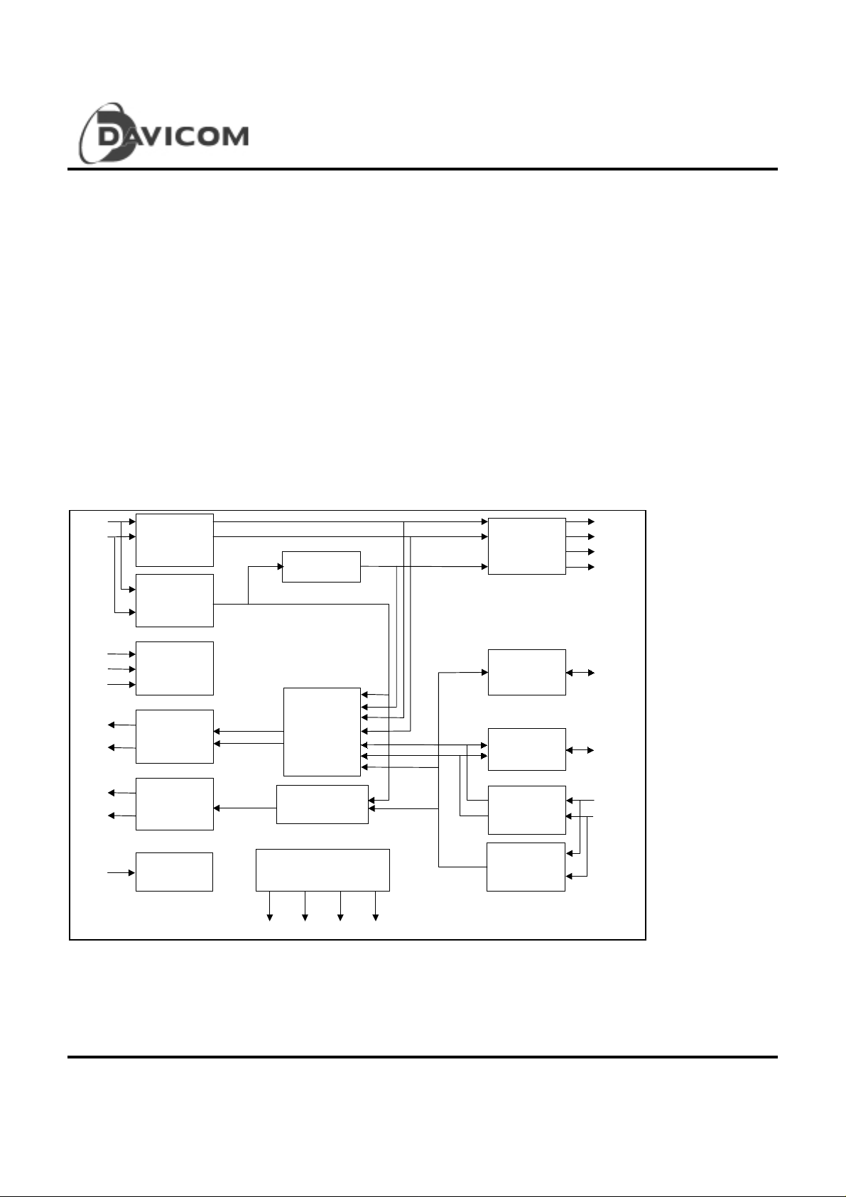
General Description
DM9095
Twisted-Pai r Medium Attachment Un it
The DM9095 twisted-pair Media Attachment Unit
(TPMAU) is designed to allow Ethernet connections
to use existing Twisted-pair wiring plants through an
Ethernet At tachment Unit Inter face (AUI). The
DM9095 provides the electrical interface between
the AUI and the twisted-pair wire.
The DM9095’s functions include level-shifted data
pass-through from one transmission media to
another, collision detection, transmitting predistortion
Block Diagram
DO +
DO -
AUI
Data
Receiver
Jabber
AUI
Data
Squelch
generation, receiving squelch function, selectable
signal-quality-error (SQE) test generation, a linkintegrity strapping option, and automatic correction
of polarity reversal on the twiste d pair input. The
DM9095 also includes LED drivers for transmit,
receive, jabber , collision, reversed polarity detect
and link status.
The DM9095 is an advanced CMOS device
available in 28-pin PLCC packages.
TP
Pre-Distortion
Driver
TPO +
DTPO +
DTPO TPO-
MD0
MD1
MD2
DI +
DI -
CI +
CI -
OSC1
Operation
Mode
Selection
AUI
Current
Driver
Collision
Current
Driver
Crystal
Oscillator
Loopback
Control
Collision
Control
LED
Drivers
RLED CLED XLED JLED
Link
Integrity
Auto-Polarity
Detection
TP
Data
Receiver
TP
Data
Squelch
LI-
AP
TPI +
TPI -
1 Final
Version: DM9095-DS-F02
August 21, 2000
Page 2

Features
DM9095
Twisted-Pai r Medium Attachment Un it
• Compatible with or exceeds IEEE 802.3
standards for AUI and 10BASE-T interfaces
• Internal pre-distortion generator for TP driver
• Smart squelch circuitry on all received data
• Selectable heartbeat function
• Selectable line-integrity test with LED indication
• LED indicator for tr ansmit, rec eiv e, jabber, and
collision
• Advanced analog CMOS process using single 5V
Pin Configuration : DM9095L
GND
1
VDD
28
TPI+
27
TPI-
26
25
24
23
LI-
DI+
DI-
5
6
7
MDO
4
DO-
3
DO+
2
supply
• Lower TP threshold option for long length
application
• Selectable auto-polarity detection and correction
function wit h LED indication
• Automatic AUI/RJ45 selection
• Power-down mode
• Full ESD protection
MD1
MD2
GND
CI+
CI-
VDD
AP
10
11
8
9
12
JLED
13
OSC1
DM9095L
14
15
GND
CLED
16
RLED
17
XLED
22
21
20
19
18
VDD
TPO-
DTPO-
DTPO+
TPO+
Final 2
Version: DM9095-DS-F02
August 21, 2000
Page 3

Twisted-Pai r Medium Attachment Un it
Pin Description
Pin No. Pin Name I/O Descriptio n
1 GND - Ground
DM9095
2
3
4 MD0 I Operation mode selection pin. Pulled high internally.
5 LI- Link-Integrity enable. The pin is a dual function pin that
6
7
8
9
DO+
DO-
DI+
DI-
CI+
CI-
I Transmitter input. A balanced differential line receiver input pair
from the AUI circuit that receives 10 Mbits/s Manchester-encoded
data and applies the data to the TP cable.
determines whether the link integrity function should be realized.
When this pin, which is internally pulled-high, is configured as an
input pin and tied low, the link integrity test function is enabled.
While configured as an output pin, the pin drives low for link-fail
state and drives high for link-pass state. The output pin can drive
an LED status indicator, as in Figure 3(b) (page 6).
O Receiver outputs. A balanced output current driver pair to the AUI
transceiver cable with the 10 Mbits/s Manchester-encoded data
received from the twisted-pair of the network.
O Collision outputs. Balanced differenti al line driver outputs which
send a 10MHz oscillation signal to the Manchester
encoder/decoder in the event of a collision, jabber interrupt, or
heartbeat test.
10 VDD - +5V Power Supply
11 AP I/O Auto Polarity. This pin is a dual func tion pin which determines if
the auto-polarity function should be enabled. The function is
enabled if the pin is HIGH. The pin is also capable of driving an
LED if the function is enabled.
12 JLED O Jabber indicator. Normally off. It indicates a time-out
transmi ssion onto TP network . It turns on i f the watchdog timer
has timed out and the twisted-pair driver has been disabled.
13 OSC1 I Crystal pin. This pin is a 20MHz frequency-reference terminal for
internal chip timing.
14 GND - Ground
3 Final
Version: DM9095-DS-F02
August 21, 2000
Page 4

DM9095
Twisted-Pai r Medium Attachment Un it
Pin Descr iption (contin ued)
Pin No. Pin Name I/O Descriptio n
15 LCED O Collision indicator. Normally off. It indicates a collision has been
detected by the M AU. It turns on the LED if a collision occurs.
16 RLED O Receive Indicator. Normally on. It indicates a reception from the
TP network is in progress. When LI- is disabled, RLED will turn
off i f the MAU receives a packet. When LI- is enabled, RLED will
turn off as long as the link is broken.
17 XLED O Transmit indicator. Normally on. It indicates that a
transmiwwion onto the TP network is in progress by turning off.
18 VDD O +5V Power Supply
19
20
21
22
23 GND - Ground
24 MD2 I Operation mode selection pin. Pulled high internally
25 MD1 I Operation mode selection pin. Pulled high internally
26
27
28 VDD O + 5V Power Supply
TPO+
DTPO+
DTPO-
TPO-
TPI-
TPI+
O TP driver outputs. These four outputs provide the TP drivers with
pre-distortion capability. The TPO+ /TPO- outputs generate
10Mbits/s Manchester- enc oded data. The DTPO+ /DTPO-
outputs are one-half bit time delayed and inverted with respect to
TPO+ /TPO-.
I TP Receive input. A differential receiver tied to the receive
transformer pair of the twisted-pair wire. The receive pair of the
twisted-pair medium is driven with 10Mbits/s Manchester-encoded
data.
Final 4
Version: DM9095-DS-F02
August 21, 2000
Page 5

Overview
DM9095
Twisted-Pai r Medium Attachment Un it
The DM9095 provi des the int erf ac e between an AUI and
a TP wire. The receive, tr ansmit, and c ollision detection
functi ons of t he DM9095 are designed t o m eet t he I EEE
802.3 10BASE-T draft standard. The receive section
transfers 10Mbits/s Manchester-encoded data from the
twisted-pair to the AUI, while the transmit section transfers
data from the AUI cable to the TP wire. The collisiondetection functi on sends a 10MHz square wav e ont o t he
AUI_CI circuits after sensing data being simultaneously
transmitted and received.
In addition to the these functions, there are three optional
operating functions. Enabling the link-integrity function
causes a pulse to be transmitted in t he absence of data
transmission. The Receiver recognized link-integrity
pulses and connects the twisted-pair link. The linkintegrity pin can be configured as an input or as an output.
When the l ink-i ntegrity pi n is confi gured as an input, the
function is enabled for proper setting. When the linkintegrity pin is configured as an output, the function is
enabled and the status of the link is indicated.
If the heartbeat function is enabled, it allows the SQE-test
sequence to be transmitted to the DTE after every
successful transmission on t he TP wi r e. The opt ion also
enables normal or ex tended line length to be selected.
When standard TP squelch levels are implemented,
normal line length is used. When the TP squelch
thresholds are lowered, extended line length is used.
The devi ce also contains an auto-polari ty func tion which
can be determined if the recei ve twisted-pair has been
wired with polarit y reversal. If the twisted-pair i s wired
with polarity reversal, the device automatically corr ec ts for
this error condit ion. Also, the auto-pol arity f unction c an
be used with an LED to display the polarity of the receive
twisted-pair wire.
When power-down m ode is set, the dev ice shuts down,
and the supply current is reduced to less than 10 µA. The
DM9095 automatically pulls AUI-DI, AUI_CI, and AUI-DO
into high impedance state if the twisted-pair link is not
connected. The function is used to provide the
Encoder/Decoder chip to use coaxial MAU. The
DM9095 also includes four drivers capable of driving four
LEDs to indicate the status of the receive, transmit,
collis io n , and jabber functions. Also, when configured
correctly, two additional LEDs can display auto-polarity
and link-integrity status.
5 Final
Version: DM9095-DS-F02
August 21, 2000
Page 6
DM9095
Twisted-Pai r Medium Attachment Un it
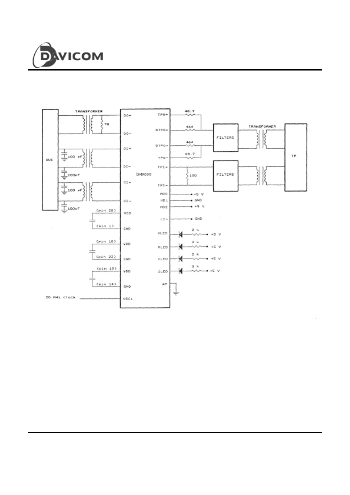
Figure 3 (a). Typical System Application for External TPMAU in Mode 5
(Where Link I ntegr ity Test is enabled, A uto-polarity is
disabled. LI- is input pin)
Final 6
Version: DM9095-DS-F02
August 21, 2000
Page 7
D
M9095
DM9095
Twisted-Pai r Medium Attachment Un it
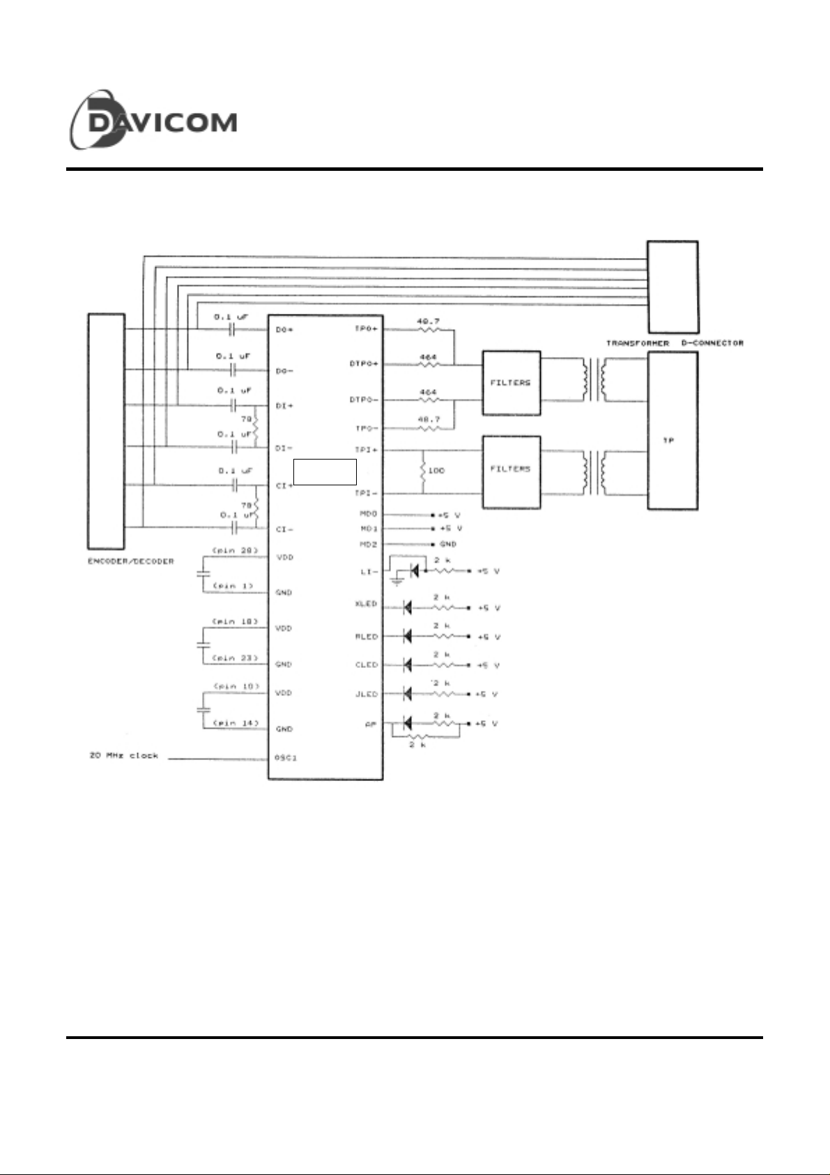
Figure 3 (b). Typical System Application for Internal TPMAU in Mode 6
(Where Lin k In tegrity Test is enabled and Auto Pola rity
Function is enabled. LI- is output pin)
7 Final
Version: DM9095-DS-F02
August 21, 2000
Page 8

Twisted-Pai r Medium Attachment Un it
Figure 4. Typical Loading Conditions for DI
²
and CI
DM9095
²
Note:
1. Pos sible filters are the Pulse Engineering Inc. <PE32101> or an equivalent.
2. The 1:1 2K V isolatio n tr ansformer can be a Pulse Engineering <PE65263> or
Equivalent.
3. The filters and isolati on transformer can be combined into one package. A
possible source is Valor Electronics <PT3877> or an equivalent.
Figure 5. Example of Transmit Circuit
Final 8
Version: DM9095-DS-F02
August 21, 2000
Page 9

DM9095
Twisted-Pai r Medium Attachment Un it
Function D escription
Transmit Funct ions
The DM9095 receives transmi t dat a f rom DO + / DO - and
transfers it to the TP network. The input must be
transformer-coupled to the AUI circuit. The receiver is able
to pass differential signals as small as 300mV peak and as
large as 1315mV. DC biasing is provided with internal
comm on-mode, the c ommon-mode is set to nominal 2. 5V .
An internal anal og delay line i s used to generate t he predistorti on signals at DTP O + and DTP O -. The DTPO + /
DTPO - signal delay s 50ns after TP O + / TPO -. A delay
lock loop, referenced to the crystal clock, is used to generate
the internal del ay line. All TP output dri ver pins are dri v er
low as a result of any of the fol lowing: t here is an AUI IDL
pulse of at least 200ns duration; the output driver is
jabbered; the l ink -integr ity opti on is enabled and there i s a
link f ail ure; or an IDL pul se is not detected at the end of a
packet and the input dose not exceed the detection
threshold of 500ns
has fini shed sending an IDL pulse onto the TP, a ti mer of
not more than 500ns is started. Whil e thi s tim er i s acti ve,
activity on the DO + / DO - inputs is ignored.
Receive Functions
The TP receiver is connected to a band-limiting filte r , w h o se
input is transformer-coupled to the twisted-pair TPI + / TPI pins. The receiver is abl e to resolve differential signals as
small as 350m V peak. Common- mode input v oltage is
provi ded with internal com mon-mode, with the commonmode set to nomi nal 2.5V. The recei ver squelch ci rcuit
prevents noise on the twisted-pair cable from falsely
triggeri ng the recei ver in the absence of true data. The
receiver will not be activated for signals at the buff er input
having a peak amplitude below 300mV, a continuous
frequency below 2 MHz, or a single cycle duration within the
pass band of the receive filter. This driver differentially
driv es a current ont o the l oad connec ted bet ween the DI +
and DI - pins. T he current through the l oad results in an
output voltage between
differentially between the two pins.
the typical loadi ng for DI + / DI - dri v er. When the dri v er
detects that it has fi nished sending an IDL pulse onto the
AUI, a timer of not more than 500ns is started. Whil e this
timer is active, activity on the TPI + / TPI - inputs is ignored,
100ns. When the driver detects that it
0.6V and 1.2V, measured
As in figure 4, it shows
and the AUI driver discharges the current stored on the
inductive load.
Collision Functions
A collis ion st ate exists whenever there are valid inputs to the
DM9095 from the network and from the DTE
simultaneously and the device is not in a link-integrity failure
state. The DM9095 reports collisions t o th e AU I by s ending
a 10 MHz signal over the CI + / CI - pair. The collision
report signal is output no more than 9 BT after the chip
detects a collision. If TPI + / TPI - become active while
there is activity on the DO + / DO - pai r , the loopback data
on TPI + / TPI - switches from transmit data to receive data
within 13 BT
/ TPI - havi ng gone idl e whil e DO + / DO – are still active,
SQE conti nues for 7 BT2 BT. If a collision condition
ex i t s wit h DO + / DO – ha vi n g gone idl e whil e T P I + / T P I –
are s till ac tive, SQE may continue for up to 9 BT.
Jabber Func tions
Jabber is a self-interrupt function that keeps a damaged
node from cont i nously t ransm it ti ng ont o the net work. The
chip c on tain s a nominal window of 50ms, during which time
a normal data li nk fram e can be transmitted. If a f rame
length exceeds this duration, the jabber function inhibits
transmi ssion and sends a collision signal on the CI + / CI –
pair. When acti vit y on the DO + / DO – pai r has ceased,
the chip cont inues to present t he CSO signal to the CI + /
CI – pair for 0.5s
pulses from the TP drivers is not inhibited when the
DM9095 is jabbed and the link integrity function is enabled.
SQE Test Functions
When the DO + / DO – pair has gone idle after a successful
tr a n s m is sion and the heartbeat function is enabled, the chip
presents the CSO si gnal to t he CI + / CI – pair. After a
successful transmi ssion onto the network medi a, the chip
presents the CSO signal within 11 BT5 BT of the end of
activity on the DO + / DO – pair. The CSO signal is
presented for 10 BT5 BT, after which the chip presents an
IDL on the CI + / CI – pair and returns to the idle state.
3 BT. If a collis ion condition exits with TPI +
50%. The transmission of l ink-int egr ity
9 Final
Version: DM9095-DS-F02
August 21, 2000
Page 10

DM9095
Twisted-Pai r Medium Attachment Un it
Link Integrity Functions
In the absence of receive traffic, the twisted-pair receiver on
the chip can detect periodic link -integrit y pulse is a 100ns
high signal wit h pre-distorti on foll owed by a return to i dle.
The chip prov ides a link-i ntegrit y reception window, during
which a link pulse is expected in t he absence of receiv e
traffic. The link-integrity window nominally opens 6.5ms
after the receipt of a link-integrity pulse or the end of a data
frame. The window closes nominally 104ms after the
receipt of a link-integrity pulse or the end of a data frame. If
a link pulse is receiv ed before the link-integrity reception
window opens, it is ignored. If no link-integrity pulse is
receiv ed while the li nk-integri ty recepti on window is open,
there is a link failure. The RLED indicator is turned off, and
the chip’s transmit, loopback, and receive functions are
disabled. If a link-integrity pulse or receive traffic is
receiv ed while the li nk-integri ty recepti on window is open,
the timers involved are reset. Once the DM9095 has
detected a link failure, one of two events must occur before
the DM9095 re-enables transmission and reception of data.
The first possible event i s the recepti on of t wo consecutive
link-integrity pulses that both fall within the link-integrity
reception window and are separated by at least a nom inal
6.5ms. The second possible ev ent is the recept ion of a
data packet from the twisted pair. With either of these
event s, the T PMAU enters a wait state and continues to
disable loopback, transmit, and receive functions. This
continues until the DM9095 determines that there is no
traff ic going in eit her the transmit or recei ve dir ection and
then enters the idle state. When the link integrity function is
enabled, the DM9095 also transmits link-integrity pulses
onto the transmit twisted-pair link. In the absence of
transmit traffic, a link-integrity pulse is transmitted at a
nominal rate of once per 16ms. Link-integrity pulses
continue to be transmi tted when the part is jabbed by the
watchdog timer or there is link-integrity failure.
of the recei ve twisted pair. When enabled, t he DM9095
powers up the function in the normal state and determines if
the receiv e wires are rev ersed. The DM9095 exam ines
either the IDL pulse at the end of each receive packet or the
link pulse when the link i ntegrity function is enabled and
uses this information to sense the polarity . If the DM9095
determines that the incoming IDL pulse is of the proper
pol ari ty, it rem ains in no rma l state. If the DM9095 detects
two consecutive reverse IDL pulses or two reverse link
pulses, it ent ers rev er se state. If the DM 9095 det erm i nes
that the polari ty of the li nk is rev ersed, it i nternal ly corr ects
for the pol ar it y, ensuri ng that all f ol l ow-on pac kets are sent
up the AUI with the correct polarity.
Automatic AUI and RJ45 Connector
Selection Functions
The chip prov ides the designer of a 10BASE-T Ethernet
interface ca rd w ith the ability to design a card without having
to provide a switch or jumper array to change between AUI
and twisted-pair connections. The DM9095 provides
automatic changeover whenever the external cable
connection is changed. When the l i nk i ntegr it y f unc ti on i s
enabled and twisted-pair cable is di sconnected, all incoming
receiv e si gnal s disappear and t he device pl aces the CI + /
CI – and DI + / DI – out puts in t hei r hi gh-i m pedance state.
In addition, DO + / DO – inputs are high-impedance inputs.
Power-Down M ode Func tion
The power-down function is ideal for embedded, laptop
computer applications. In power-down mode, the chip
pulls withi n 10uA. W hen the devi ce is reactiv ated from
power-down mode, normal transceiver operation will
resume after the 3.2ms calibration sequence is completed.
Power-On Reset Function
Auto-Polarity Detection and
Correction Functions
The DM9095 can det erm i ne i f the rec eive twisted pai r has
been wired with a polarity reversal. If so, the DM9095
automatically corrects for this error condition, when the
correcti on functi on is enabled. Also, the AP pin it self c an
be connected to an LED to display the status of the polarity
Final 10
Version: DM9095-DS-F02
August 21, 2000
The DM9095 uses a power-on reset sequence to place itself
into a known digit al state, t o allow the analog sections to
sta biliz e , and to calibrate the internal delay line. Depending
on the power-down condition, initialization requires the
following lengths of time:
z
Power-on reset: 3.2 ms
z
Power-down mode: 3.2 ms
Page 11

Crystal Oscillator
An external TTL-Level clock can be applied to the
OSC1 pin which is crystal oscillator input. A resistor
should be added in series with the clock source to limit
the ampl itude of t he voltage swing seen by the pin.
A 500 resistor works well in most cases.
DM9095
Twisted-Pai r Medium Attachment Un it
integrity function is enabled. If LI- is connected to
DD
or left floating (internal pull-high), the link
V
integrity function is disabled. When configured as an
output pin, the pin drives low for link-fail state and
drives high for link-pass state. The output pin can
drive an LED status indicator.
LED Status Functions
The LED drivers requi re an ex t ernal resistor in seri es
with the LED, which is in turn connected to VDD.
The driv er pulls the pi n low to light t he LED and can
sink up to 15mA of drive current from the resistor with
an output impedance of less than 50. The
DM9095 provides three types LED drivers, as follows.
Output LED Dri ver s: The LED output s XLED, RLED,
JLED, and CLED are output LED drivers. These
signals are used f or status inform ation only. XLED
drives high when the DM9095 is transmitting a packet.
XLED is not asserted if the DM9095 has detect ed a
jabber f unction or is in a l ink-fai l state. RLED drives
high when the DM9095 is receivi ng a packet . RLED
is not asserted when the DM9095 is in a link-fail state.
JLED drives low when the DM9095 has detected a
jabber condition. CLED drives low when the
DM9095 has detected a collision condition.
Sampled LED Dri ver: The AP pin is used to set the
configuration of the DM9095 and drive the LED status
indicat ors. Ev ery 26ms, the pi n is conf igured as an
input pin for 6.5• s. During this time, it is sampled by
the DM9095. Outside the sampling window, the
driv er is placed in an out put state and used to driv e
the LED indi cator s. AP i s dri ven low to i ndic ate that
a reversed twisted pair has been detected on the
receive circuit and corrected. If AP is tied low,
DM9095 disables the auto-pol ari t y f unct i on; when AP
is pulled high externally, the function is enabled.
Input / Output LED Driver: LI-pin is an input/output
pin, depending on the mode selection. When
configured as an input pin, LI-controls the link integrity
test option. If LI- is connected to GND, the link
Mode MD0 MD1 MD2
0000 No Extended I Long wire TP
1001 No Normal INormal wire TP
2010 No Normal OLI pin LED output
3011 Poer-down mode
4100 Yes Extended I Long wire TP
5101 Yes Normal INormal wire TP
6110 Yes Normal OLI pin LED output
7111 Power-down mode
Heartbeat Line Length LI- Application
Power
There are six power connections to the DM9095,
including three VDD and three GND connections.
Pins 1 and 28 are used f or anal og suppli es, inc ludi ng
squelch circuits, receiver, and the internal delay
circui t. Pi ns 10 and 14 are used for di gital circuits,
the I/O buffer, the control logic for analog circuits, and
the crystal oscillator circuit. Pins 18 and 23 are used
for the Twisted Pair driver output buffer.
Operating Modes
The mode selection pins are used to select one of
eight operating modes. These modes are
summarized in the table below.
The modes referred to in the table are the following:
z
Heartbeat: A Yest means that the heartbeat
functi on is enabled; A No means the
heartbeat function is di sabl ed.
z
Line Length: “Extended” indicates that TP receive
squelch thresholds have been
lowered to 300mV for use with longer
line lengths; Normal indicates that the
standard 10BASE-T TP receive
squelch threshold of 450mV will be
used.
z
LI-: The LI - pin can be c onfigured t o be an input
pin, whereby the link-integrity function can be
enabled or disabled. The LI- pin can also be
configured as an output pin to indicate the
status of the link, where the link-integrity is
enabled.
Mode Description
11 Final
Version: DM9095-DS-F02
August 21, 2000
Page 12

DM9095
Twisted-Pai r Medium Attachment Un it
AC Electrical Characteristics
Symbol Parameter Min. Typ. Max. Unit
Transmi t Tim ing
TD
t
TLB
t
TPDY
t
TOFF
t
TIDL
t
Receive Timing
RD
t
ROFF
t
RIDL
t
Collision Timin g
CB
t
CE
t
Transmi t delay fr om DO² to TPO
Loopback delay from DO² to DI
²
²
0 200 ns
0 500 ns
DTPO - to TPO + and DTPO + to TPO - delay 47 53 ns
DO + high to idle time 200 ns
TPO + high to idle time 250 350 ns
Receive delay from TPI² to DI
²
0 500 ns
TPI + high to idle time 200 ns
DI + high to idle time 250 350 ns
Collision turn-o n time 0 90 0 ns
Collision turn-o ff time 0 90 0 ns
CLB
t
CIDL
t
CPH
t
CP
t
Loopback delay when switching from DO² to TPI
CI + high to idle time 250 350 ns
Collision high-pulse width 40 50 60 ns
Collision period 80 100 120 ns
²
1000 1600 ns
Jabber Timing
JMT
t
JCB
t
JU
t
Final 12
Version: DM9095-DS-F02
August 21, 2000
Maximum transmit time for TPO
Time from Jabber to enable CI² output
Unjab time 250 450 750 ms
²
45 50 55 ms
0 900 ns
Page 13

DM9095
Twisted-Pai r Medium Attachment Un it
AC Electrical Characteristics (continued)
Symbol Parameter Min. Typ. Max. Unit
Link Integrity Timing
LP
t
LPWT
t
Transmitted link integrity pulse period 8 16 24 ms
Link integrity pulse width for TPO + 80 100 120 ns
LPWD
t
Heartbeat Timing
HD
t
HCS
t
LED Timing
XSET
t
XOFF
t
XON
t
ROFF
t
RON
t
RLFSET
t
RLFOFF
t
Link integrity pulse width for DTPO
²
40 50 60 ns
Heartbeat turn-on time 600 1600 ns
Heartbeat active time for CI² output
500 1500 ns
XLED turn-off time 10 • s
XLED off time 90 110 ms
XLED minimum on time 4 8 ms
RLED off time 90 110 ms
RLED min i mum on ti me 4 8 ms
RLED turn-off time for link fail 50 150 ms
RLED off time for link fail
RLFON
t
CSET
t
CON
t
JSET
t
JON
t
13 Final
RLED on time for link success 0.5 1.5 s
CLED turn-on time 10 • s
CLED nominal on time 10 20 ms
JLED turn-on time 10 • s
JLED on time 250 750 ms
Version: DM9095-DS-F02
August 21, 2000
Page 14

Timi ng Waveforms
DM9095
Twisted-Pai r Medium Attachment Un it
Final 14
Version: DM9095-DS-F02
August 21, 2000
Page 15

DM9095
Twisted-Pai r Medium Attachment Un it
15 Final
Version: DM9095-DS-F02
August 21, 2000
Page 16

Timi ng Waveforms (continued)
DM9095
Twisted-Pai r Medium Attachment Un it
Final 16
Version: DM9095-DS-F02
August 21, 2000
Page 17

Timi ng Waveforms (continued)
Figure 10. Transmitted link integrity pulse timing
DM9095
Twisted-Pai r Medium Attachment Un it
17 Final
Version: DM9095-DS-F02
August 21, 2000
Page 18

Timi ng Waveforms (continued)
DM9095
Twisted-Pai r Medium Attachment Un it
Final 18
Version: DM9095-DS-F02
August 21, 2000
Page 19

Timi ng Waveforms (continued)
DM9095
Twisted-Pai r Medium Attachment Un it
19 Final
Version: DM9095-DS-F02
August 21, 2000
Page 20

DM9095
Twisted-Pai r Medium Attachment Un it
Package Information
PLCC 28L Outline Dimensions unit: inch/mm
Note:
1. Dimension D & E do not i nclude resin fin.
D
2. Dimensions G
mount pad pitch desig n reference only.
Final 20
Version: DM9095-DS-F02
August 21, 2000
& GE are for PC Board surface
Page 21

DM9095
Twisted-Pai r Medium Attachment Un it
Ordering Information
Part Num ber Pin Count Package
DM9095L 28 PLCC
Disclaimer
The information appearing in this publication i s believed to
be accurate. Integrated circuits sold by DAVICOM
Semiconductor are covered by the warranty and patent
indemnification provisions stipulated in the terms of sale
only. DAVICOM makes no warranty, express, statutory,
implied or by description regarding the information in this
publication or regarding the information in this publication or
regarding the freedom of the described chip(s) from patent
infringement. FURTHER, DAVICOM MAKES NO
WARRANTY OF MERCHANTABILITY OR FITNESS
FOR ANY PURPOSE. DAVICOM deserves the right to halt
production or alter the specifications and prices at any time
without notice. Accordingly, the reader is cautioned to verify
that the data sheets and other information in this publication
are current before placing orders. Products de scribed herein
are intended for use in normal commercial applica tions.
Applications involving unusual environmental or reliability
requirements, e.g. military equipment or medical life
support equipment, are specifically not recommended
without additional processing by DAVICOM for such
applications. Please note that application circuits illustrated
in this document are for reference purposes only.
DAVICOM’s terms and conditions printed on the order
acknowledgment govern all sales by DAVICOM.
DAVIC OM will not be bound by any terms inconsistent with
these unless DAVICOM agrees otherwise in writing.
Acceptance of the buyer’s orders shall be based on these
terms.
Company Ov erview
DAVICOM Semiconductor, Inc. develops and
manufactures integrated circuits for integration into data
communica tion pro ducts. O ur mission is to design and
produce IC products that re the industry’s best value for
Data, Audio, Video, and Internet/Intranet applications. To
achieve this goal, we have built an organization that is able
to develop chipsets in response to the evolving technology
requirements of our customers while still delivering p r oduct s
that meet their cost requirements.
Products
We offer only products that sati sfy high performance
requirements and which are compatible with major
hardware and software standards. Our currently available
and soon to be released products are based on our
proprietary designs and deliver high quality, h igh
performance chipsets that comply with modem
communication standards and Ethernet networking
standards.
Contact Windows
For additional information about DAVICOM products, contact the sales departme nt at:
Headquar ter s
Hsin-chu Office:
3F, No. 7-2, Industry E. Rd., IX,
Science-based Park,
Hsin-c hu C ity, Taiw an , R.O.C .
TEL: 886-3-5798797
FAX: 886-3-5798858
WARNING
Conditions beyond those listed for the absolute maximum may destroy or damage the produ cts. In addition, conditions for su stained periods at near the limits
of the operating ra nges will stress and may tempo rarily (and perm anently) affect and damage structure, performance and/or function.
21 Final
Taipei Sales & Marketing Office:
8F, No. 3, Lane 235, Bao-chiao
Rd.,
Hsin-tie n, Taip ei, Taiw an , R.O.C .
TEL: 886-2-29153030
FAX: 886-2-29157575
Email: sales@davicom.com.tw
Davicom USA
Sunnyvale, California
1135 Kern Ave., Sunnyvale,
CA94085, U.S.A.
TEL: 1-408-7368600
FAX: 1-408-7368688
Email: sales@davicom8.com
Version: DM9095-DS-F02
August 21, 2000
 Loading...