

Page 1
General Descriptio n
DM9008
ISA/Plug & Play Super Ethernet Contoller
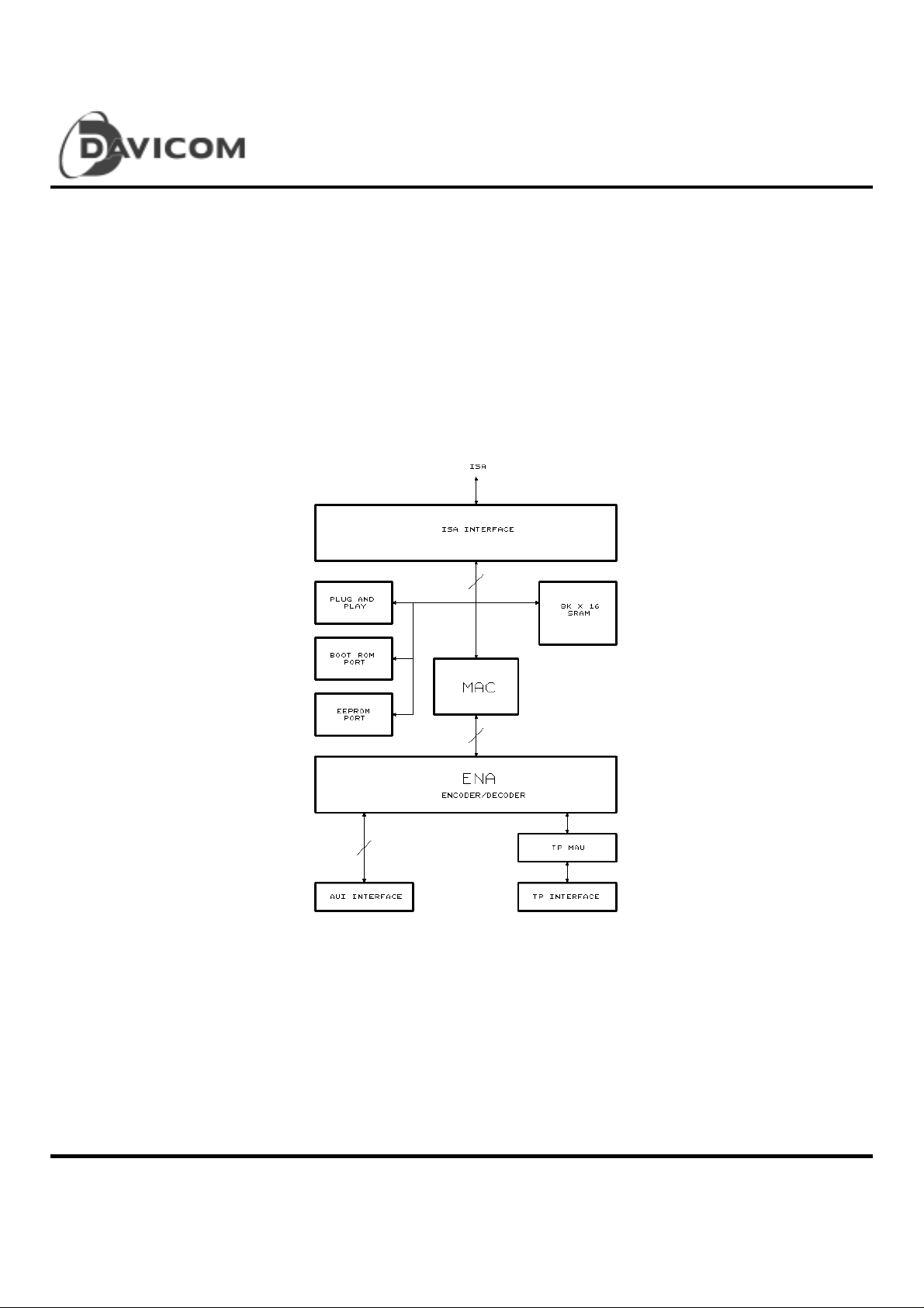
The DM9008 Ethernet controller is a highly integrated design
that provides all Medial Access Control (MAC)
and Encode-Decode (ENDEC) functions in accordance with
the IEEE 802.3 standard. Network interfaces
include 10BASE5 or 10BASE2 Ethernet via the AUI
port and 10BASE-T via the Twisted-pair. The DM9008
Ethernet controller can interface directly to the PC-AT
ISA bus without any external device. The interface to
PC-AT ISA bus is fully compatible with NE2000 Ethernet
Block Diagram
adapter cards, so all software programs designed for NE2000
can run on the DM9008 card without any modification.
Microsoft's Plug and Play and the jumperless software
configuration function are both suppo rted. The capab ility o f the
PnP and Non-PnP mode auto-switch function allows users to
con f igur e network card . No jumpers or swit ches ar e needed to
set when using either the PC
or PnP function. The integrated 8Kx16 SRAM and 10BASE-T
tr ansceiver make D M9008 more co s t-effective .
Final 1
Version :D M 90 08-DS-F02
June 14, 2000
Page 2
Features
Single chip solution for IEEE 802.3, 10BASE-T,
10BASE2 and 10BASE5
Integrated ISA interface, 8Kx16 SRAM, Media Access
Control, ENDEC and 10BASE-T transceiver
Supports ISA Plug and Play configuration
Software-compat ible w i th NOVELL NE2000
Supports PnP and Non-PnP Auto-switching
PnP, Non-PnP and Auto-switch mode software
selectable
8 interrupt lines selectable
Auto-Polarity detection and correction
Selectable 8 and 16-bit slot mode
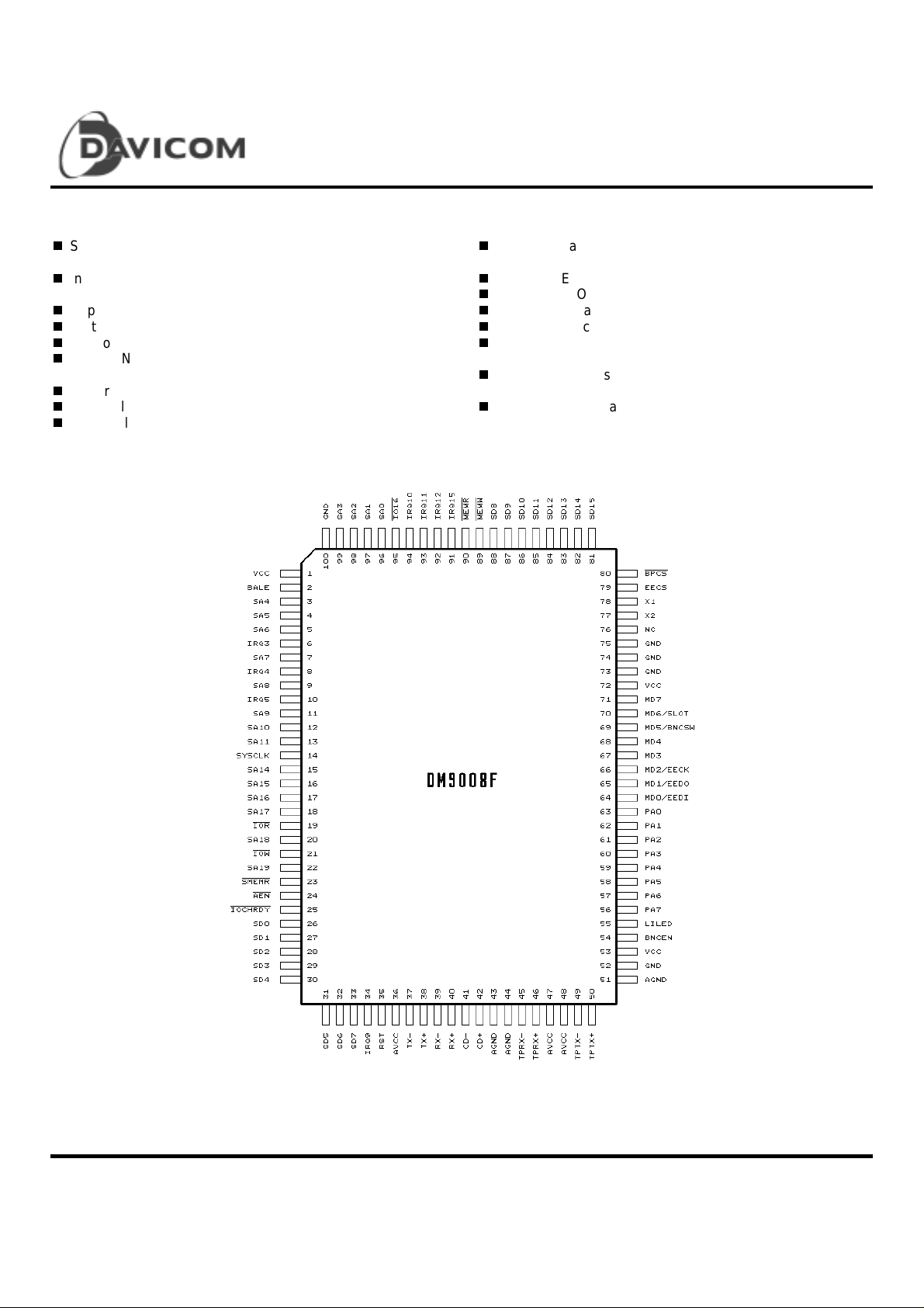
Pin Co nfigurati o n
DM9008
ISA/Plug & Play Super Ethernet Contoller
Provides auto-detection/auto-switching for 10BASE-T
Transceiver and Attachment Unit Interface (AUI)
External EEPROM programmable
Supports BOOT-ROM page mode
Loopback capability for diagnostics
Receiver and collision squelch circuit to reduce noise
Low-power CMOS process with single 5V power
supply
Built-in pre-distortion resisters for 10BASE-T
application
100-pin QFP package
2 Final
Version :D M 90 08-DS-F02
June 14, 2000
Page 3

Absolute Maximum Ratings*
DM9008
ISA/Plug & Play Super Ethernet Contoller
*Comments
Supply Voltage (VCC) . . . . . . . . . . . . . . . . -0.5V to +7.0V
DC Input Voltage (Vin) . . . . . . . . . . . -0.5V to VCC +0.5V
DC Output Voltage (Vout) . . . . . . . . . -0.5V to VCC +0.5V
Storage Temperature Range (Tstg) . . . -65°C to + 150°C
Power Dissipation (PD) . . . . . . . . . . . . . . . . . . . . 500 mW
Lead Temp. (TL) (Soldering, 10 sec.) . . . . . . . . . . 235°C
Case Temp. (Tc) . . . . . . . . . . . . . . . . . . . . . . 0°C to 85°C
ESD rating (Rzap = 1.5k, Czap = 120 pF) . . . . . . . 4000V
Differential Input Voltage . . . . . . . . . . . . . . . -5.5V to 16V
Differential Output Voltage . . . . . . . . . . . . . . . . 0V to 16V
DC Electrical Characteristics
Symbol Parameter Min. Max. Unit Conditions
Voh High Level Output Voltage
(Notes 1, 2)
Vol Low Level Output Voltage
(Notes 1, 2)
Vih High Level Input Voltage (Note 6) 3.0 V
Vil Low Level Input Voltage (Note 6) 0.8 V
Iin Input Current -1.0 +1.0
(VCC = 5V ± 5%, Tc= 0°C to 85°C, unless otherwise specified)
VCC - 0.1
3.5
Stresses above those listed under "Absolute Maximum
Ratings" may cause permanent damage to this device. These
are stress ratings only. Functional operation of this device at
these or any other conditions above those indicated in the
operational sections of this specification is not implied or
intended. Exposure to the abso lute maxi mum ra ting co nditions
for extended periods may affect device reliability.
0.1
0.4
V
V
V
V
µA
Ioh = -20µA
Ioh = -2.0mA
Iol = 20µA
Iol = 2.0mA
Vi = VCC or GND
Ioz Tri-state Output Leakage Current -10 +10
Icco Operating VCC + AVCC Supply
Curren t (Note 3)
Iccs Standby VCC + AVCC Supply
Curren t (Note 4)
Differential Pins (TX+/TX-, RX+/RX-, CD+/CD)
V
OD
V
OB
V
U
Dif feren tial Output Voltage (TX±)
Differential Output Voltage
Im balance (TX±)
Undershoot Voltage (TX±)
+550 +1200 mV 78 ohm termination and
µA
120 mA
110 mA
40 mV 78 ohm termination and
100 mV 78 ohm termination and
Vout = VCC or GND
X1 = 20 Mhz
Iout = 0µA
Vin = VCC or GND
270 ohms from each to GND
270 ohms from each to GND
270 ohms from each to GND
Final 3
Version :D M 90 08-DS-F02
June 14, 2000
Page 4

ISA/Plug & Play Super Ethernet Contoller
DC Electrical Characteristics (continued)
Symbol Parameter Min. Max. Unit Conditions
DM9008
VDS
VCM Differential Input Common Mode
Twisted Pair Interface Pins (TPTX+/TPTX-)
Vtidf TP input voltage .350 2.0 V -
Vil
Vih
Note 1: These levels are tested dynamically using a limited number of functional test patterns. Refer to AC Test Load.
Note 2: The low drive CMOS compatible Voh and Vol limits are not tested directly. Detailed device characterization verifies
Note 3: This measurement is made while the DM9008 is undergoing transmission, reception, and collision. The value is
Note 4: This measurement is made while the DM9008 is sitting idle of transmission. This measurement is described in note
Not e 5: T his param eter is guaranteed b y design and is not tested.
Note 6: Except RST, IOR B, IOWB which are Schmitt trigger with Vil = 1 . 0V, Vih = 2.8 V .
Dif feren tial Squelch Th reshold (R X±
and CD±)
Voltage (RX± and CD±) (Note 5)
LI:
low
high
that this specification can be guaranteed by testing the high dr ive TTL compatibl e Vol and Voh specific ations.
not measured instantaneously, but is averaged over a span of several milliseconds.
1.
-175
(No te 5)
05.5V
-
2.4
-300 mV
0.8
-
V
V
-
-
4 Final
Version :D M 90 08-DS-F02
June 14, 2000
Page 5

ISA/Plug & Play Super Ethernet Contoller
Pin Description
Pin No. Symbol I/O Description
PC ISA BUS INTERFACE PINS
DM9008
96 - 99
3 - 5
7
9
11 - 13
15 - 18
20, 22
26 - 33
88 - 81
2 BALE I ADDRESS LATCH ENABLE: PC ISA bus BALE signal; used only to
14 SYSCLK I SYSTEM CLOCK: PC ISA bus system clock
19
21
SA0 - SA3
SA4 - SA6
SA7
SA8
SA9 - SA11
SA14 - SA17
SA18, SA19
SD0 - SD7
SD8 - SD15
IOR
IOW
I SYSTEM ADDRESS: These signals are connected to the address
bus of the PC I/O slot. The y are use d to se lect the D M9008 I/O ports
or the boot ROM address
I/O, Z SYSTEM DATA: These signals are connected to the data bus of the
PC I/O bu s slot. They are used to transfer data between the PC and
the DM9008
define the timing of IOCHRDY in Remote DMA
This pin is not used if the value of biteA of CRB is 0, and tie to high to
prevent floating.
This pin is not used if the value of biteA of CRB is 0, and tie to high to
prevent floating.
I I/O READ: An active low signal used to read data from the DM9008
I I/O WRITE: An active low signal used to write data to the DM9008
23
35 RST I RESET: An active high signal used to power-on reset the DM9008
24
25
89
90
95
Final 5
Version :D M 90 08-DS-F02
June 14, 2000
SMEMR
AEN
IOCHRDY
MEMW
MEMR
IO16
I MEMORY READ: An acti v e low signal used to r ead boot ROM data
I ADDRESS ENABLE: This is an active low signal used to enable the
system address for the DM9008
O I, Z I/O CHANNEL READY: The DM9008 sets this signal low to insert
wait states into the PC ISA bus
I MEMORY WRITE: PC ISA bus memory write signal
This pin is not used if the value of biteA of CRB is 0, and tie to high to
prevent floating.
I MEMORY READ: PC ISA bus memory read signal
This pin is not used if the value of biteA of CRB is 0, and tie to high to
prevent floating.
O, Z 16-BIT I/O: This signal goes low when the data transfer between the
DM9008 and the PC ISA bus is word wide
Page 6

DM9008
ISA/Plug & Play Super Ethernet Contoller
6
8
10
34
94 - 92
91
MEMORY INTERFACE PINS
79 EECS O EEPROM CHIP SELECT: This signal goes high when the EEPROM
80
64 - 71
(64)
(65)
(66)
(66)
(69)
(70)
IRQ3
IRQ4
IRQ5
IRQ9
IRQ10-12
IRQ15
BPCS
MD0 - MD7
(EEDI)
(EEDO)
(EECK)
(LEDSW)
(BNCSW)
(SLOT)
O, Z INTERRUPT REQUESTS: These are 8 interrupt request pins. Only
one pin, which is decoded from Configuration Register A, can be
activat ed; the other pins are left fl oating. The activat ed pin will go
high when an interrupt request is generated from the ENC module of
the DM9008
is selected by the DM9008
O BOOT ROM CHIP SELECT: This signal goes low when the PC
reads the boot ROM data
I/O, Z MEMORY DATA BUS: These are the memory data signals for the
boot ROM
When the EEPROM is loaded or written, MD0, 1, 2 are used as the
EEPROM signals
* EEPROM DATA IN: This pin is used as the serial input data
signal from the EEPROM
* EEPROM DATA OUT: This pin is used as the serial output data
signal to the EEPROM
* EEPROM CLOCK: This pin is used as the EEPROM clock signal
These memory data pins can also be used as switches when the
DM9008 is in reset state. There is an approximately 100K pull-low
resistor on eac h pin, and a 10K pull- high resist or can be connec ted
to a pin when i t is switched to logic h igh
LED mode switch: see page 67 for details.
* When this pin pulled high upon reset, pin 54 outputs 312.5KHz
* SLOT SELECTION: When this pin is pulled to high, the DM9008 is
in NE2000 16-bit mode
63 - 56 PA0 - PA7 O BOOT ROM PAGE ADDRESS. When the boot ROM is accessed,
PA0-PA7 are used as the page address of the boot ROM
NETWORK INTERFACE PINS
37
38
54 BNCEN O BNC OUTPUT ENABLE: This pin goes high if the value of the
78 X1 O CRYSTAL FEEDBACK OUTPUT: Used in crystal connection only.
77 X2 I CRYSTAL or EXTERNAL CLOCK INPUT
6 Final
TX-
TX+
O TRANSMIT OUTPUT: Differential line driver which sends the
encoded data to the transceiver. The outputs are source followers
which require 270 ohm pull-down resistors
Configuration Register B bit 1 is low and bit 0 is high. Typically, this
pin is used to control the DC-DC converter to enable or disable the
UM9092A (Coax ial Transceiver Interface)
* Output 312.5KHz clock: when the 69 pin (BNCSW) is pulled high,
this pin output 312.5KHz clock
Connect to ground when using an external clock
Version :D M 90 08-DS-F02
June 14, 2000
Page 7

ISA/Plug & Play Super Ethernet Contoller
Pin Description (continued)
Pin No. Symbol I/O Description
NETWORK INTERFACE PINS
DM9008
39
40
41
42
50
49
46
45
5 LILED OPEN
76 NC No connection
POWER SUPPLY PINS
36, 47, 48 AVCC +5V DC power supply for analog CKT. A decoupling capacitor
43, 44, 51 AGND GND for analog CKT
RX-
RX+
CD-
CD+
TPTX+
TPTX-
TPRX+
TPRX-
I RECEIVE INPUT: Differential receive input pair from the transceiver
I COLLISION INPUT: Differential collision input pair from the
transceiver
O TP Driver Outputs. These two outputs provide the TP drivers with
pre-distortion capability
I TP Receive Input. A differential receiver tie to the receive
transformer pair of the twisted-pair wire.
The receive pair of the twisted-pair medium is driven with 10
Mbits/s Manchester-encoded data
LINK and Traffic LED Driver: If TP is LINK-pass, this pin outputs low.
DRAIN
This pin will go low for 80ms and then into high impedance state for
50ms to indicate th e presence of t raffic on t he network
should be connected between these pins and GND for analog CKT
1, 53, 72 VCC +5V DC power supply for digita l CKT . A decoupl ing capac i tor sho uld
be connected between these pins and GND for digital CKT
52, 73, 74,
75, 100
Final 7
Version :D M 90 08-DS-F02
June 14, 2000
GND GN D for digital CKT
Page 8

ENC Register Address Assignments
DM9008
ISA/Plug & Play Super Ethernet Contoller
Page 0 (PS1 = 0, PS0 = 0)
SA0-SA3 RD WR
00H Command (CR) Command (CR)
01H Current Local DM A
Address 0 (CLDA0)
02H Current Local DM A
Address 1 (CLDA1)
03H Boundary Pointer
(BNRY)
04H Transmit Status
Register (TSR )
05H
06H FIFO
07H Interrupt Status
08H Current Remote
09H Current Remote
0AH Configura tion
0BH Configura tion
0CH Receive Status
0DH Tally Counter 0
0EH
0FH
Number of
Collisions Register
(NCR)
Register (ISR)
DMA Address 0
(CRDA0)
DMA Address 1
(CRDA1)
Register A
Register B
Register (RSR )
(Frame AlignmentÞ
Errors) (CNTR 0 )
Tally Counter 1
(CRC Errors)
(CNTR1)
Tally Counter 2
(Missed Packet
Errors) (CNTR 2 )
Page Start Register
(PSTART)
Page Stop Register
(PSTOP)
Boundary
Pointer(BNRY)
Transmit Page Start
Address (TPSR)
Transmit Byte
Count Register 0
(TBCR0)
Transmit Byte
Count Register 1
(TBCR1)
Interrupt Status
Register (ISR)
Remote Start
Address Register 0
(RSAR0)
Remote Start
Address Register 1
(RSAR1)
Remote Byte Count
Register 0 (RBCR0)
Remote Byte Count
Register 1 (RBCR1)
Receive Configuration Register (RCR)
Transmit
Configuration
Register (TCR)
Data Configuration
Register (DCR)
Interr u p t Mask
Register ( IMR )
Page 1 (PS1 = 0, PS0 = 1)
SA0-SA3 RD WR
00H Command (CR) Command (CR)
01H
02H Physical Address
03H Physical Address
04H
05H
06H Physical Address
07H Current Page
08H
09H Multicast Address
0AH Multicast Address
0BH Multicast Address
0CH
0DH Multicast Address
0EH Multicast Address
0FH
Physical Address
Register 0 (PAR0)
Register 1 (PAR1)
Register 2 (PAR2)
Physical Address
Register 3 (PAR3)
Physical Address
Register 4 (PAR4)
Register 5 (PAR5)
Register (CURR)
Mult ic ast Address
Register 0 (MA R0)
Register 1 (MA R1)
Register 2 (MA R2)
Register 3 (MA R3)
Mult ic ast Address
Register 4 (MA R4)
Register 5 (MA R5)
Register 6 (MA R6)
Mult ic ast Address
Register 7 (MA R7)
Physical Address
Register 0 (PAR0)
Physical Address
Register 1 (PAR1)
Physical Address
Register 2 (PAR2)
Physical Address
Register 3 (PAR3)
Physical Address
Register 4 (PAR4)
Physical Address
Register 5 (PAR5)
Current Page
Register (CURR)
Register 0
(MAR0)Multicast
Address
Mult ic ast Address
Register 1 (MA R1)
Mult ic ast Address
Register 2 (MA R2)
Mult ic ast Address
Register 3 (MA R3)
Mult ic ast Address
Register 4 (MA R4)
Mult ic ast Address
Register 5 (MA R5)
Mult ic ast Address
Register 6 (MA R6)
Mult ic ast Address
Register 7 (MA R7)
8 Final
Version :D M 90 08-DS-F02
June 14, 2000
Page 9

Register Address Assignments (continued)
Page 2 (PS1 = 1, PS0 = 0)
DM9008
ISA/Plug & Play Super Ethernet Contoller
SA0-SA3 RD WR
00H Command (CR) Command (CR)
01H ³
02H Page Stop
03H Remote Next
04H
05H Local Next Pac ket Local Next Pac ket
06H Address Counter
07H
08H ---- ---09H Interrupt Lines
0AH
Page Start
Register (PSTART)
Register (PSTOP)
Packet Pointer
Transmit Page
Start Address
(Upper)
Address Counter
(Lower)
Status Register
Boot ROM Page
Register
Current Local D MA
Address 0 (CLDA0)
Current Local D MA
Address 1 (CLDA1)
Remote Next
Packet Pointer
----
Address Counter
(Upper)
Address Counter
(Lower)
Interrupt Lines
Pull-Down Register
Boot ROM Page
Register
SA0-SA3 RD WR
0BH Configuration
Register C
0CH
0DH
0EH Data Configuration
0FH Interrupt Mask
Receive
Configuration
Register (RCR)
Transmit
Configuration
Register (TCR)
Register (DCR)
Register ( IMR )
Configuration
Register C
Page3 (PS1=1, PS0=1)
SA0-SA3 RD WR
00H Command (CR) Command (CR)
01H-06H ---- ----
07H Configuration
Register D
08H-0FH ---- ----
Configuration
Register D
----
----
----
----
Final 9
Version :D M 90 08-DS-F02
June 14, 2000
Page 10

DM9008
ISA/Plug & Play Super Ethernet Contoller
Register Descriptions
Configuration Register A (CRA)
Configuration Register A can be read at address 0AH in Page 0 of ENC, and can be writte n by following a read to address 0AH with a
write to address 0AH. If address 0AH is written without a previous read to 0AH, the write will be regarded as a write to register RBCR0
of ENC.
76543210
FREAD INT2 INT1 INT0 IOAD3 IOAD2 IOAD1 IOAD0
Bit Symbol Description
0 - 3 IOAD0
IOAD1
IOAD2
IOAD3
4 - 6 INT0
INT1
INT2
I/O Address: Th ese thr ee bits deter min e t he bas e I/O address of D M 9008 within the PC
system's I/O map
bit3 bit2 bit1 bit0 I/O base
0 0 0 0 300H
0 0 0 1 320H
0 0 1 0 340H
0 0 1 1 360H
0 1 0 0 380H
0 1 0 1 3A0H
0 1 1 0 3C0H
0 1 1 1 3E0H
bit3 bit2 bit1 bit0 I/O base
1 0 0 0 200H
1 0 0 1 220H
1 0 1 0 240H
1 0 1 1 260H
1 1 0 0 280H
1 1 0 1 2A0H
1 1 1 0 2C0H
1 1 1 1 2E0H
Interrupt Pin Mapping: Only one interrupt output pin will be driven active when a valid
interrupt condition occurs
bit5 bit4 bit3 Interrupt
0 0 0 IRQ3
0 0 1 IRQ4
0 1 0 IRQ5
0 1 1 IRQ9
1 0 0 IRQ10
1 0 1 IRQ11
1 1 0 IRQ12
1 1 1 IRQ15
7 FREA D Fas t Read : In t h e r emo t e DM A rea d mod e. W hen t hi s bit is set high, the DM9008 will begin
the next port fetch before the current
10 Final
is completed
IOR
Version :D M 90 08-DS-F02
June 14, 2000
Page 11

DM9008
ISA/Plug & Play Super Ethernet Contoller
Configuration Regi st er B (CRB)
Configuration Register B can be read at address 0BH in Page 0 of ENC, and can b e written b y following a r ead to address 0BH with a
write to address 0BH. If a write to address 0BH is perform ed without a previous read to 0BH, it will be regarded as a write to register
RBCR1 of ENC.
765 4321 0
-- -- BUSERR CHRDY -- GDLINK PHYS1 PHYS0
Bit Symbol Description
0, 1 PHYS0
PHYS1
2 GDLINK Read: Link status. One indicates Link OK; zero indicates Link Fail
3 -- Reserved
4 CHRDY
5 BUSERR Bus Error: This bit shows that DM9008 has detected an ISA bus error. This bit will be high if
6 -- Reserved
7 -- Reserved
Physical Media Interfaces: These two bits determine which type of physical interface the
DM9008 is using, as shown below:
bit1 bit0 Interface
0 0 Set to 10BASE-T; BNCEN = low
0 1 Set to 10BASE2; BNCEN = high
1 0 Set to 10BASE5; BNCEN = low
1 1 Auto-detection media
or
IOCHRDY from
the command strob e. If high, IOCHRDY will be pulled low after BALE goes high
DM9008 inserts wait states into a system access and the system terminates the cycle without
inserting wait states
IOR
or from BALE: When low, DM9008 will pull IOCHRDY low after
IOW
Final 11
Version :D M 90 08-DS-F02
June 14, 2000
Page 12

Configuration Register C (CONFIG.C)
This register is configured during RESET and EEPROM rea d sta tes.
CONFI G.C can be r e a d from address 0BH of page 2 of ENC.
76 54321 0
-- PnP -- -- BPS3 BPS2 BPS1 BPS0
Bit Symbol Description
DM9008
ISA/Plug & Play Super Ethernet Contoller
0 - 3 BPS0
BPS1
BPS2
BPS3
4 - 5 -- Reserved
6 PnP DM9008 is in PnP state when this bit is set
7 -- Reserved
BOOT PROM Select: Selects address at which boot ROM begins and size of boot ROM
bit3 bit2 bit1 bit0 Address Size
0 0 0 X X No boot ROM
0 0 1 0 C0000H 16K
0 0 1 1 C4000H 16K
0 1 0 0 C8000H 16K
0 1 0 1 CC000H 16K
0 1 1 0 D0000H 16K
0 1 1 1 D4000H 16K
1 0 0 0 D8000H 16K
1 0 0 1 DC000H 16K
1 0 1 0 C0000H 32K
1 0 1 1 C8000H 32K
1 1 0 0 D0000H 32K
1 1 0 1 D8000H 32K
1 1 1 0 C0000H 64K
1 1 1 1 D0000H 64K
These four bits can be updated by writing new values to this register
12 Final
Version :D M 90 08-DS-F02
June 14, 2000
Page 13

ISA/Plug & Play Super Ethernet Contoller
Configuration Register D (CONFIG. D)
This register can be read or written at register 07H of ENC Page 3. All bits of this register are power-on low.
76 54321 0
EEMODE -- -- CLK-REF EECS EECK EEDO EEDI
Bit Symbol Description
0 EEDI EEPROM DATA IN: This bit reflects the st at e of the DM9008 MD0 pin
1 EEDO EEPROM DATA OUT: When EEMODE is high, this bit reflects the state of the DM9008 MD1
pin
2 EECK EEPROM CLOCK: When EEMODE is high, this bit reflects the state of the DM9008 MD2 pin
3 EECS EEPROM CHIP SELECT: When EEMODE is high, this bit reflects the state of the DM9008
EECS pin
DM9008
4CLK-REF
5, 6 -- Res erved. Mus t be set to zero
7 EEMODE EEPROM MODE: If this bit is set high, the EEPROM can be programmed with the values of
When EEMODE is hi gh, thi s bit is t oggled every 12µs
EECS, EECK and EEDO in this register
Final 13
Version :D M 90 08-DS-F02
June 14, 2000
Page 14
DM9008
ISA/Plug & Play Super Ethernet Contoller
Interrupt Line Sta tus Re gister
The logic value of DM9008's eight interrupt pins can be read in register 09H o f ENC, page 2.
76 54321 0
IRQ15 IRQ12 IRQ11 IRQ10 IRQ9 IRQ5 IRQ4 IRQ3
Bit Symbol Description
0 - 7 IRQ3-15 INTERRUPT LINE STATUS: The logic values of interrupt pins IRQ3-15
Interrupt Line Pull-Down Register
When any one o f the eight bit s in re gister 09H of ENC page 2 is set to one , the co rrespond ing in terrupt line w ill be pul led down to GND
with a resistor whose value is approximatel y 1K. All bi ts of this register are power-on low.
76 5432 10
IRQPD15 IRQPD12 IRQPD11 IRQPD10 IRQPD9 IRQPD5 IRQPD4 IRQPD3
Bit Symbol Description
0 - 7 IRQ PD3-15 INTERRUPT LINE PULL-DOWN: When one, enables the interrupt line to be pulled down
with 1K resistor
Boot ROM Page Register
The boot ROM page register can be read or written in register 0AH of ENC page 2.
All bits of this register are power-on low.
7 654321 0
XMA8 XMA7 XMA6 XMA5 XMA4 XMA3 XMA2 XMA1
Bit Symbol Description
0 - 7 XMA1-8 B OOT ROM PAGE ADDRESS: When boot ROM is read by host, the value of this register will
be indicated by MEMORY ADDRESS PA0-7
14 Final
Version :D M 90 08-DS-F02
June 14, 2000
Page 15

Command Register (CR)
DM9008
ISA/Plug & Play Super Ethernet Contoller
The Command Register is used to initiate transmissions,
enable or disable Remote DM A operation s, and se le ct registe r
pages. To issue a command, the microprocessor sets the
corresponding bit(s) (RD2, RD1, RD0, TXP). Further
commands may be ove rlappe d, but w ith the fo llowing rules: (1)
If a transmit command overlaps a remote DMA operation, bits
RD0, RD1, and RD2 must be maintained for the remote DMA
command when the TXP bit is set. Note that if a remote DMA
command is re-issued when the transmit command is given,
7 65432 10
PS1 PS0 RD2 RD1 RD0 TXP STA STP
Bit Symbol Description
D0 STP
D1 STA Start mode
D2 TXP Transmi t Packe t: T his bit mus t be se t to in itia te tran smi ss ion of a pack et . TXP is inte rna lly res et
STOP: Software reset command. Takes the controller off-line, and no packets will be received
or transmitted. Any reception or transmission in progress will continue to completion before the
reset stat e is enter ed. To exi t this st ate, th e STP bit m ust be res et. The so ftwar e res et is
execu t ed on l y wh en i n di c at ed b y t he R ST bi t in the ISR b ei n g set t o a " 1. " STP pow er s u p
high
after the transmission is either completed or aborted. This bit should be set only after the
Transmit Byte Count and Transmit Page Start registers have been programmed. TXP powers
up low
the DMA will be completed immediately if the remote byte
count register has not been reinitialized. (2) If a remote DMA
operation overlaps a transmission, RD0, RD1, and RD2 may
be written with the desired values and a "0" may be written to
the TXP bit. Writing a "0" to this bit has no effect. (3) A remote
write DMA may not overlap a remote read operation or vice
versa. Either of these operations must either be completed or
be aborted before the other operation may start. Bits PS1,
PS0, RD2 and STP may be set at any time.
D3
D4
D5
D6
D7
Final 15
Version :D M 90 08-DS-F02
June 14, 2000
RD0
RD1
RD2
PS0
PS1
Remote DMA Command: These three encoded bits control operation of the Remote DMA
channel. RD2 can be set to abort any Remote DMA co mmand in progress. The Remote
Byte Count Registers should be cleared when a Remote DMA has been aborted. The
Remote Start Addresses are not restored to the starting address if the Remo t e DMA is
aborted. RD2 powers up high
RD2 RD1 RD0
0 0 0 Not Allowed
0 0 1 Remote Read
0 1 0 Remote Write
0 1 1 Send Packet
1 X X Abort/Complete Remote DMA
Page Select: T hese two enco ded bits select which registe r page is to be accessed wit h
addresses SA0-3
PS1 PS0
0 0 Register Page 0
0 1 Register Page 1
1 0 Register Page 2
1 1 Register Page 3
Page 16

DM9008
ISA/Plug & Play Super Ethernet Contoller
Data Configure Register (DCR)
This register is used to program the DM9008 for the 8 or 16-bit memory interface, select byte ordering in 16-bit applications, and
establish FIFO thresholds. The DCR must be initialized prior to loading the Remote Byte Count Registers. LAS is set on power up.
7 65432 10
-- FT1 FT0 ARM LS LAS BOS WTS
Bit Symbol Description
D0 WTS Wor d Transfer S elect
0: S elect s 8-bit DMA tra nsfer s
1: Selects 16-bit DMA transfers
D1 BOS Byte Order Select
0: MS byte placed on SD15-SD8 and LS byte on SD7-SD0 (32000, 8086)
1: MS byte placed on SD7-SD0 and LS byte on SD15-SD8 (68000)
Ignored when byte-wide DMA operation is chosen
Note: Byte Order Select mode is not supported in the current version of the DM9008, so
this bit should be cleared in the application
D2 LAS Long Add ress Select
0: Dual 16-bit DMA mode
1: Single 32-bit DMA mode
Note: Single 32-bit DMA mode is not supported in the current version of the DM9008, so
this bit should be cleared in the application
D3 LS Loopback Select
0: Loopback mode selected. Bits D1, D2 of the TCR must also be programmed for
Loopback mode selected
1: Normal Operation
D4 ARM Auto-initialize Remote
0: Send Command not executed, all packets removed from Buffer Ring under program
control
1: Send Command executed, Remote DMA auto-initialized to remove packets from Buffer
Ring
D5
D6
D7 -- Reserved
FT0
FT1
FIFO Threshold Select: Encoded FIFO threshold. During reception, the FIFO threshold
indicates the number of bytes (or words) filled into the FIFO serially from the network
before received data are written to the buffer RAM
Rec eive Thresholds
FT1 FT0 Word Wide Byte Wide
0 0 1 Word 2 Bytes
0 1 2 Words 4 Bytes
1 0 4 Words 8 Bytes
1 1 6 Words 12 Bytes
During transmission, the FIFO threshold indicates the number of bytes (or words filled into
the FIFO fro m the Loca l DMA before transmitted da ta are read fro m the buffer RAM . Thus,
the transmission threshold is 16 bytes less than the receive th reshold
16 Final
Version :D M 90 08-DS-F02
June 14, 2000
Page 17

DM9008
ISA/Plug & Play Super Ethernet Contoller
Transmit Configuration Register (TCR)
The transmit configuration register deter mines the actions of the transmitter se ction of the DM9008 du ring transmiss ion of a packet on
the network. LB1 and LB0 power up as 0.
7 65432 10
-- -- -- OFST ATD LB1 LB0 CRC
Bit Symbol Description
D0 CRC Inhibit CRC
0: CRC appended by transmitter
1: CRC inhibited by transmitter
D1
D2
D3 ATD Auto Transmit Disable: This bit allows another station to disable the DM9008 transmitter by
D4 OFST Collision Offset Enable: This bit modifies the backoff algorithm to allow propitiation of
D5 -- Reserve must be set to zero
D6 -- Reserved
LB0
LB1
Encoded Loopback Con trol: These encode d con figuration bits se t the type of loop back that
is to be performed. Note that loopback in mode 2 sets the ENA in loopback mode and
that D3 of the DCR must be set to zero for loopback operation
LB1 LB0
Mode 0 0 0 Normal Operation
Mode 1 0 1 ENC module Loopback
Mode 2 1 0 ENA module Loopback
Mode 3 1 1 Loopback to Coax
transmission of a particular multicast packet. The transmitter can be re-enabled by
resetting this bit or by reception of a second particular multicast packet
0: Normal Operation
1: Reception of multicast address hashing to bit 62 disables transmitter; reception of
multicast address hashing to bit 63 enables transmitter
nodes
0: Ba ckoff Logi c implements normal algori thm
1: Forces Backoff algorithm modification to 0 to 2
three collisions, then follows standard backoff. (For first three collisions, station has
higher average backoff delay, resulting in a low priority mode.)
min(3+n,10)
slot times for first
D7 -- Reserved
Final 17
Version :D M 90 08-DS-F02
June 14, 2000
Page 18

Transmit Status Register (TSR)
DM9008
ISA/Plug & Play Super Ethernet Contoller
This register records events that occur on the media during
transmission of a packet. It is cleared when the next
transmission is initiated by the host.
All bits remain low un less t he event that corresponds to
7 654321 0
OWC CDH FU CRS ABT COL -- PTX
Bit Symbol Description
D0 PTX Packet Transmitted: Indicates transmission without error (no excessive colli-sions or FIFO
underrun) (ABT ="0", FU ="0")
D1 -- Reserved
D2 COL Transmit Collided: Indicates that transmission collided at least once with another station on
the ne tw ork . The nu mb e r of collis io ns is recorded in the Number of Colli-sions Register (NCR)
D3 ABT Transmit Aborted: Indicates the DM9008 aborted transmission because of excessive
collisions (total number of transmissions including original transm i ssion at tem p t e quals 16)
D4 CRS Carrier Sense Lost: This bit is set when carrier is lost during transmission of the packet.
Car rier S ense is m onitor ed from the end of Pream ble/ Sync h until the end of tr ansmis sion.
Transmission is not aborted on loss of carrier
a particular bit occurs during transmission. Each transmission
should be followed by a read of this register. The contents of
this register are not specified until after the first transmission.
D5 FU FI FO Underrun: If the ENC cannot gain access to the bus before the FIF emp ties , this bit is
set. Transmission of the packet will be aborted
D6 CDH CD Heartbeat: Failure of the transceiver to transmit a collision signal after transmission of a
packet will set this bit. The Collision Detect (CD) heartbeat signal must commenc e d uring the
first 6 .4µs of the interframe gap followinga transmission. In certain collisions, the CD heartbeat
bit will be set even though the transceiver is not performing the CD heartbeat test
D7 OWC
Out of Window Collision: Indicates that a collision occurred after a slot time (51.2µs).
Transmi ssions are r escheduled as in normal colli s ions
18 Final
Version :D M 90 08-DS-F02
June 14, 2000
Page 19

DM9008
ISA/Plug & Play Super Ethernet Contoller
Receive Configuration Register (RCR)
This register deter mines the opera tion of the NIC during rece ption of a packe t, and is used to program what types o f packets to ac ce pt.
7 65432 10
-- -- MON PRO AM ABP ARP SEP
Bit Symbol Description
D0 SEP Save Errored Packets
0: Packets with receive errors are rejected
1: P ackets with receive erro rs are acc epted. Receive er rors are CRC and Fr ame
Alignment errors
D1 ARP Accept Runt Packets
0: Packets with fewer than 64 bytes rejected
1: Packets with fewer than 64 bytes accepted
D2 ABP Accept Broadcast
0: Packets with all 1's broadcast destination address rejected
1: Packets with all 1's broadcast destination address accepted
D3 AM Accept Multicast
0: Packets with multicast destination address not checked
1: Packets with multicast destination address checked
D4 PRO Promiscuous Physical
0: Physical address of node must match the station address programmed in PARO PAR5 (physical address checked)
1: All packets with physical address accepted (physical address not checked)
D5 MON Monitor Mode: Enables the receiver to check addresses and CRC on incoming packets
without buffering to memory. The Missed Packet Tally counter will be incremented for each
recognized packet
0: Packets buffered to memory
1: Packets checked for address match, good CRC and Frame Alignment, but not buffered
to memory
D6 -- R eserve: must be set to zero
D7 -- Reserved
Note: D2 and D3 are "OR'd" together, i.e., if D2 and D3 are set, DM9008 will accept broadcast and multicast
addresses, as well as its own physical address. To establish full promiscuous mode, bits D2, D3, and D4
should be set. In addition, the multicast hashing array must be set to all 1's to accept all multicast addresses
Final 19
Version :D M 90 08-DS-F02
June 14, 2000
Page 20

Receive Status Register (RSR)
DM9008
ISA/Plug & Play Super Ethernet Contoller
This register records the status of the received packet,
including information on errors and the type of address match,
eit her ph ysica l or mul ticas t. The co ntent s of thi s regis ter a re
written to buffer memory by the DMA after reception of a good
packet. If packets with errors are to be saved, the receive
status is written to memory at the head of the erroneous packet
if an erroneous packet is received.
76 54321 0
DFR DIS PHY MPA FO FAE CRC PRX
Bit Symbol Description
D0 PRX Pac ket Received Intact: lnd icates packet received without error. (Bit s CRC, FAE, FO, and
MPA are zero for t he received p acket.)
D1 CRC CRC Error: Indicates packet recei ved with CRC error. Increm ents Tally Counter ( CNTR1).
This bit will also be set for F rame Alignment errors
D2 FAE Frame Alignment Error: Indicates that the incoming packet did not end on a byte boundary and
the CRC did not match at last byte boundary. I ncrements Tally counte r ( CNTRO)
D3 FO FIFO Overrun: This bit is set when the FIFO is not serviced, causing overflow during
reception. Reception of the packet will be aborted
D4 MPA Missed Packet: Set when packet intended for node cannot be accepted by the DM9008
because of a lack of receive buffers, or when the controller is in monitor mode and did not
buffer the packet to memory. Increments Tally Counter (CNTR2)
If packets with errors are to be rejected, the RSR will not be
written to memory. The contents will be cleared when the next
packet arrives. CRC errors, frame alignment errors and missed
packets are counted internally by DM9008, which releases the
host from reading the RSR in real time to record errors for
network management functions. The contents of this register
are not specified until after the first reception.
D5 PHY
D6 DIS Receiver Di sabl ed: Set when receiver is disabled by e ntering M onito r mode
D7 DFR Deferring: Set when the carrier or collision signal is detected by ENC. If the transceiver has
Note: The following co di ng appli es t o CRC and FAE bits:
FAE CRC Type of Error
0 0 No error (Good CRC and <6 Dribble Bits)
0 1 CRC ERROR
1 0 Illegal, will not occur
1 1 Frame Alignment Error and CRC Error
20 Final
Phy sical /Mult icas t Ad dress: Ind icates whether received packet had a phys i cal or m ulticast
address type
0: Physical Address Match
1: Multicast/Broadcast Address Match
Reset when receiver is re-enabled while exiting Monitor mode
asserted the CD line as a result of the jabber, this bit will stay set, indicating the jabber
condition
Version :D M 90 08-DS-F02
June 14, 2000
Page 21

Interrupt Mask Register (IMR)
DM9008
ISA/Plug & Play Super Ethernet Contoller
The Interrupt Mask Register is used to mask interrupts. Each
interrupt mask bit corresponds to a bit in the Interrupt Status
Register (ISR). If an interrupt mask bit is set, an interrupt will be
76 54321 0
-- RDCE CNTE OVWE TXEE RXEE PTXE PRXE
Bit Symbol Description
D0 PRXE PACKET RECEIVED INTERRUPT ENABLE
Enables interrupt when packet is received
D1 PTXE PACKET TRANSMITTED INTERRUPT ENABLE
Enables interrupt when packet is transmitted
D2 RXEE RECEIVE ERROR INTERRUPT ENABLE
Enables interrupt when packet is rece ived with error
D3 TXEE TRANSMIT ERROR INTERRUPT ENABLE
Enables interrupt when packet transmission results in error
D4 OVWE OVERWRITE WARNING INTERRUPT ENABLE
Enables interrupt when Buffer Management Logic lacks sufficient buffers to store
incoming packet
issued whenever the corresponding bit in the ISR is set. If any
bit in the IMR is set low, an interrupt will not occu r whe n the bit
in the ISR is set. The IMR powers up all zeroes.
D5 CNTE COUNTER OVERFLOW INTERRUPT ENABLE
Enables interrupt when MSB of one or more of the Network Tally counters has been set
D6 RDCE DMA COMPLETE INTERRUPT ENABLE
Enables interrupt when Remote DMA transfer has been completed
D7 -- Reserved
Final 21
Version :D M 90 08-DS-F02
June 14, 2000
Page 22

Interrupt Status Register (ISR)
DM9008
ISA/Plug & Play Super Ethernet Contoller
This register is accessed to determine the cause of an
interrupt. Any interrupt can be masked in the interrupt Mask
Register (IMR). Individual interrupt bits are cleared by writing a
1 to the corresponding bit of the ISR.
76 54321 0
RST RDC CNT OVW TXE RXE PTX PRX
Bit Symbol Description
D0 PRX Packet Received : lndicates packe t re ceived with no errors
D1 P TX Pack et Tra nsmit ted: l ndic ates pa c ket t ransmitted with no errors
D2 RXE Receive Error: lndicates that a packet was received with one or more of the following errors:
-- CRC Error
-- F rame Al ignment Err or
-- FIFO Overrun
-- Missed Packet
D3 TXE Transmit Error: Set when packet is transmitted with one or more of the following errors:
-- Excessive Collisions
-- FIFO Underrun
The IRQ signal is ac tive as lo ng as any unmaske d s ign al i s se t,
and will not go low until all unmasked bits in this register have
been cleared.
The ISR must be cleared after power up by writing it with all
1's.
D4 O VW Overwrite Warning: Set when receive buffer ring storage resources have been exhausted.
(Local DMA has reached Boundary Pointer.)
D5 CNT Counter Overflow: Set when MSB of one or more of the Network Tally Counters has been set
D6 RDC Remote DMA Complete: Set when Remote DMA operation has been completed
D7 RST Reset Status: A status indicator (no interrupt generated):
-- Set when E N C enters reset stat e and cleared when a start command is issu ed.
-- Set when a Receive Buffer Ring overflows and cleared when overflow status ends
Writing to this bit has no effect. The bit powers up high
22 Final
Version :D M 90 08-DS-F02
June 14, 2000
Page 23

Network Tally Counter Registers (CNTR)
DM9008
ISA/Plug & Play Super Ethernet Contoller
Physical Address Regist er (PAR0-PAR5)
Three 8-bit counters are provided for monitoring the number of
CRC errors, Frame Alignment Errors and Missed Packets. The
maximum count reached by any counter is 192 (C0H). These
regist ers will be cleared when read by the CPU. The count is
recorded in binary in CT0-CT7 of each Tally Register.
CNTR 0: Mo nitors the number of Frame Ali gnment errors
76543210
CT7 CT6 CT5 CT4 CT3 CT2 CT1 CT0
CNTR 1: Mo ni tor s the number of CRC err ors
76543210
CT7 CT6 CT5 CT4 CT3 CT2 CT1 CT0
CNTR 2: Monitors the number of Missed Packets
76543210
CT7 CT6 CT5 CT4 CT3 CT2 CT1 CT0
Number of Collisions Register (NCR)
This register contains the number of collisions a node
experiences when attempting to transmit a packet. If no
collisions are experienced during a transmission attempt, the
COL bit of the TSR will not be set and the contents of NCR will
be zero . If ther e are exces sive c ollisi ons, th e ABT bit in t he
TSR will b e set and the cont ents of NCR will be zero. NCR is
cleared after TXP in CR is set.
7654321 0
NCR 0 0 0 0 NC3 NC2 NC1 NC0
FIFO Re gis t e r ( FIFO)
The Physical Address Registers are used to compare the
destination addresses of incoming packets to be rejected or
accepted. Comparisons are performed on a byte-wide basis.
The bit assignment shown below relates the sequence in
PAR0-PAR5 to the bit sequenc e of the received pack et.
. . SynSynDA0 DA1 DA2 DA3 DA4 DA5 DA6 DA7 . .
Destinatio n Address Sou
D7 D6 D5 D4 D3 D2 D1 D0
PAR0 DA7 DA6 DA5 DA4 DA3 DA2 DA1 DA0
PAR1 DA15 DA14 DA13 DA12 DA11 DA10 DA9 DA8
PAR2 DA23 DA22 DA21 DA20 DA19 DA18 DA17 DA16
PAR3 DA31 DA30 DA29 DA28 DA27 DA26 DA25 DA24
PAR4 DA39 DA38 DA37 DA36 DA35 DA34 DA33 DA32
PAR5 DA47 DA46 DA45 DA44 DA43 DA42 DA41 DA40
Multicast Address Registers (MAR0-MAR7)
The Mu lti cast Addr ess Reg ist ers pr ovid e fil teri ng of m ult icast
addresses hashed by the CRC logic. All destination addresses
are fed through the CRC logic. When the last bit of the
destination address enters the CRC, the 6 most significant bits
of the CRC generator are latched. These 6 bits are then
decoded by a 1 of 64 decode to index a uniqu e f ilter b i t (F B 0 -
63) in the multicast address registers. If the filter bit selected is
set, the multicast packet is accepted. The system designer
uses a program to determine which filter bits to set in the
multicast registers. If an address is found to hash to the value
50(32H), then FB50 in MAR6 should be initialized to 1. All
multicast filter bits that correspond to the multicast address
accepted by the node are then set to one. To accept all
multicast packets, al l of the registers are set to all ones.
Thi s is an 8-bi t reg ist er t hat all ows t he CP U to exa mi ne t he
content s of the FIFO after loopback. The FI FO will cont ai n th e
last 8 data bytes transmitted in the loopback packet.
Sequential reads from the FIFO will advance a pointer in the
FIFO and allow reading of all 8 bytes. Note that the FIFO
should only be read when DM9008 has been programmed in
loopback mode.
76543210
DB7 DB6 DB5 DB4 DB3 DB2 DB1 DB0
Final 23
Version :D M 90 08-DS-F02
June 14, 2000
Page 24

D7 D6 D5 D4 D3 D2 D1 D0
MAR0 FB7 FB6 FB5 FB4 FB3 FB2 FB1 FB0
MAR1 FB15 FB14 FB13 FB12 FB11 FB10 FB9 FB8
MAR2 FB23 FB22 FB21 FB20 FB19 FB18 FB17 FB16
MAR3 FB31 FB30 FB29 FB28 FB27 FB26 FB25 FB24
MAR4 FB39 FB38 FB37 FB36 FB35 FB34 FB33 FB32
MAR5 FB47 FB46 FB45 FB44 FB43 FB42 FB41 FB40
MAR6 FB55 FB54 FB53 FB52 FB51 FB50 FB49 FB48
MAR7 FB63 FB62 FB61 FB60 FB59 FB58 FB57 FB56
DMA Registers
Local DMA Transmit Registers
15 8 7 0
DM9008
ISA/Plug & Play Super Ethernet Contoller
(i) Local DMA Transmit Regi st ers
Transmit Page Start Register (TPSR)
This regi ster point s to th e assembled pac ket to be t ransmitted.
Since all transmit packets are assembled on 256-byte page
boundaries, only the eight higher order addresses are
specified.
76543210
A15 A14 A13 A12 A11 A10 A9 A8
Transmit Byte Counter Register 0,1 (TBCR0,TBCR1)
These two r egisters indicate the length of the p acket to be
transmitted in bytes. The maximum number of transmit bytes
allowed is 64K bytes. The DM9008 will not truncate
transmissions longer than 1500 bytes.
76543210
TBCR1 L15 L14 L13 L12 L11 L10 L9 L8
(TPSR) PAGE START
(TBCR0,1) TRANSMIT BYTE COUNT
Local DMA Receive Registers
15 8 7 0
(PSTART) PAGE START
(PSTOP) PAGE STOP
(CURR) CURRENT
(BRNY) BOUNDARY
(CLDA0,1) CURRENT LOCAL DMA ADDRESS
Remote DMA Registers
15 8 7 0
(RSAR0,1) START ADDRESS
(RBCR0,1) BYTE COUNT
76543210
TBCR0 L7 L6 L5 L4 L3 L2 L1 L0
(ii) Local DMA Receive Registers
Page Start, Stop Registers (PSTART, PSTOP)
The Page Start and Page Stop Registers program the starting
and stopping page of the Receive Buffer RAM. Since the
DM9008 uses fixed 256-byte buffers aligned on page
boundaries, only the upper eight bits of the start and stop
address are specified.
76543210
PSTART
PSTOP
A15 A14 A13 A12 A11 A10 A9 A8
Boundary Register (BNRY)
This register is used to prevent overflow of the Receive Buff e r
Ring. Buffer management compares the contents of this
register to the next buffer address when linking buffers
tog eth er. If the c onten ts of th is reg iste r mat ch the next bu ffe r
address, the local DMA operation is aborted.
7654321 0
BNRY A15 A14 A13 A12 A11 A10 A9 A8
(CRAD0,1) CURRENT REMOTE DMA ADDRESS
24 Final
Version :D M 90 08-DS-F02
June 14, 2000
Page 25

Current Page Register (CURR)
This register is used internally by the Buffer Management
Logic as a backup register for reception. CURR contains the
address of the first buffer to be used for a packet reception,
and is used to restore DMA pointers in the event of receive
errors. This register is initialized to the same value as
PSTART, and should not be written to again unless the
controller is reset.
DM9008
ISA/Plug & Play Super Ethernet Contoller
76543210
RSAR1 A15 A14 A13 A12 A11 A10 A9 A8
76543210
RSAR0A7A6A5A4A3A2A1A0
76543210
CURR A15 A14 A13 A12 A11 A10 A9 A8
Current Local DMA Register 0, 1 (CLDA0, 1)
These two registers can be accessed to deter mine the current
Local DMA Address.
76543210
CLDA1A15 A14 A13 A12 A11 A10 A9 A8
76543210
CLDA0A7 A6 A5 A4 A3 A2 A1 A0
(iii) Remote DMA Registers
Remote Start Address Registers (RSAR0, 1)
Remote Byte Count Registers (RBCR0, 1)
Remote DMA operations are programmed via the Remote
Start Address (RSAR0, 1) and Remote Byte Count registers
(RBCR0, 1). The Remote Start Address is used to point to the
start of the block of data to be transferred. The Remote Byte
Count is used to indicate the length of the b lock (in bytes).
76543210
RBCR1 BC15 BC14 BC13 BC12 BC11 BC10 BC9 BC8
³
76543210
RBCR0 BC7 BC6 BC5 BC4 BC3 BC2 BC1 BC0
Current Remote DMA Address Registers (CRDA0, 1)
The Cu rrent Remote DM A Regist ers con tain th e curr ent
address of the Remote DMA. The bit assignments are
shown below:
76543210
CRDA1 A15 A14 A13 A12 A11 A10 A9 A8
76543210
CRDA0 A7 A6 A5 A4 A3 A2 A1 A0
Final 25
Version :D M 90 08-DS-F02
June 14, 2000
Page 26

DM9008
ISA/Plug & Play Super Ethernet Contoller
Functional Description
Plug and Play (PnP) Module
Auto-c onfigurat i on Ports
Three 8-bit I/O ports are defined for the PnP read/write operations. They are called "Auto-configuration ports", and are listed below.
Port Name Type Location
ADDRESS W 279H (Pr inter status po r t)
WRITE DATA W A79H (Printer status prot + 800H)
READ DATA R Relocatable in range 203H to 3FFH
The Plug and Play registers are accessed by first writing the
address of the desired register, which is called the "Register
Index". This can be followed by any number of WRITE_DATA
or READ_DATA accesses to the same indexed register
without any need to writ e to the ADDRESS port before each
access.
The Address port is also the write destination of the initiation
key, which will be descri b ed later.
Plug and Play Registers
The Plug and Play registers may be divided into two groups:
card registers and logical device registers. According to the
Plug and Play specification, for each additional device
contained in a PnP card, there should be a corresponding copy
of the logical device register. However, because the DM9008
contains only one logical device, the card registers and logical
device registe rs are unique fo r ea ch ca rd. Those PnP registe rs
or bits not defined in the following table are all read with value
= 0.
26 Final
Version :D M 90 08-DS-F02
June 14, 2000
Page 27

ISA/Plug & Play Super Ethernet Contoller
Card Control Registers
Index Name Type Definition
00H Set RD_DATA port W The location of the READ_DATA port is determined by
writing to this register. Bits[7:0] become ISA I/O read port
address bits[9:2]. Address bits[1:0] of the READ_DATA port
are always1
01H Serial Isolation R A read to this register causes a PnP card in the Isolation state
to c ompar e one bit of the c ard's ser ial I D. This pr ocess is
described in more detail on page 34
02H Config Control W Bit[0] - Reset command
Settin g this bit will reset all logical devices and restore
con f igurati on regi ster s to thei r power -up values
The CSN is pr eserved
Bit [1] - Wait fo r Key command
Setting this bit makes the PnP card return to the Wait for
Key state. The CSN is preserved
Bit[2] - Pn P Reset CSN command
Setting this bit will reset the card's CSN to 0
Not e that the ha rdware will automatic a lly clear t he bits
without any need for software to clear them
DM9008
03H W ake[ CSN] W A writ e to thi s regi ster will cau se all cards that ha ve a C SN
that matches the write data[7:0] to go from the Sleep state to
either the 1) I solation s tate if the wri te dat a for t his command
is zero, o r 2) Config state if t he write data is not zer o
04H Resource Data R A read from this regis ter reads the nex t byte of resou rce data.
The Status register must be polled until bit[0] is set before this
register may be read
05H Status R Bit[0], wh e n se t, in di ca te s i t is O.K . to read the next data b y te
from the Resource Data register
06H Card Select Numbe
(CSN)
07H Logical Device R 00H (Only one logical device in DM9008)
R/W A write to thi s regi ster s ets a card's CSN. The CSN's value is
uniquely assigned to each ISA PnP card after the serial
iden ti fi cat ion pro ces s so that ea ch car d may be ind iv idu all y
selected during a Wake[CSN] command
Final 27
Version :D M 90 08-DS-F02
June 14, 2000
Page 28

ISA/Plug & Play Super Ethernet Contoller
Logical Device Control Registers
Index Name Type Definition
30H Activate R/W For each logical device, there is one Activate register that
controls whether or not the device is active on the ISA bus.
Bit[0], if set, activates the logical device. Before a logical
device i s activated, I/O range check must be disable d
31H I/O Range Check R/W Thi s register is used to perform a conflict check on the I/O
port range programmed for use by a logical device
Bit[1] - This bit, when set, enables I/O range check
I/O range check is only valid when the logical device is
inactive
Bit[0] - If set, this bit fo r ces logic al device t o respond to I/O
reads within logical device's assigned I/O range w i th
a55H when I/O range check is in operation. If clear, the
logical device drives AAH
Logical Device Configuration Registers
Memory Configuration Registers
DM9008
Index Name Type Definition
40H BROM base address
bits[23:16]
41H BROM base address
bits[15:0]
42H Memory Control R 00H (Only 8-bit operation is supported for BROM)
R/W Bits[23:20] and bit[17] are read only when their values = 0.
All other bits ar e read/write bits
R/W Bits[1 3:8] are read only when th eir values = 0.
All other bits ar e read/write bits
I/O Conf i guratio n Registers
Index Name Type Definition
60H I/O base address
bits[15:8]
61H I/O base address
bits[7:0]
R/W Bits[15:10] are read-only with undete rmined values. Bit[9] is
read only, and is always 1.
All other bits ar e read/write bits
R/W Bits[4:0] are read only when their values = 0.
All other bits ar e read/write bits
28 Final
Version :D M 90 08-DS-F02
June 14, 2000
Page 29

ISA/Plug & Play Super Ethernet Contoller
Interrupt Configuration Registers
Index Name Type Definition
70H IRQ level R/W Read/write value indicating a selected interrupt level.
Bits[3:0] se lect which ISA in terru p t level is used. A value of 1
selects IRQ1, 15 selects IRQ15, etc. IRQ0 is not a valid
interrupt s election
DM9008
71H IRQ type
bits[7:0]
R Read/write value indicating which type of interrupt is used
for the IRQ selected above.
Bit[1] - Level, 1 = high, 0 = low
Bit[0] - Type, 1= level, 0 = edge
For DM90 08, this register is read only, with a value of 02H
DMA Configuration Registers
Index Name Type Definition
74H DMA channel select 0 R 04H (indicating no DMA channel is needed)
75H DMA channel select 1 R 04H (indicating no DMA channel is needed)
Vendor Define d Regist ers
Index Name Type Definition
F0H CONFIG A R Direct mapping of CONFIG A register, page 0
F1H CONFIG B R Direct mapping of CONFIG B register, page 0
F2H CONFI G C R Direct mapping of the CONFIG C register, page 2
F4H RESET CSN W Writing bit 2 to 1 will reset DM9008 CSN to 0
Final 29
Version :D M 90 08-DS-F02
June 14, 2000
Page 30

Initial Values of CONFIG.A-D after PC Hardware Reset
CONFIG A
Bit 7 Bit 6 Bit 5 Bit 4 Bit 3 Bit 2 Bit 1 Bit 0
Mode FREAD INT2 INT1 INT0 IOAD3 IOAD2 IOAD1 IOAD0
DM9008
ISA/Plug & Play Super Ethernet Contoller
DM Jumperless
Plug and Play
CONFIG B
Mode -- -- BUSERR CHRDY -- GDLINK PHYS1 PHYS0
DM Jumperless
Plug and Play
CONFIG C
Mode -- PnP-B -- -- BPS3 BPS2 BPS1 BPS0
DM Jumperless
Plug and Play
CONFIG D
Mode EEMODE -- -- CLK-REF EECS EECK EEDO EEDI
9346 9346 9346 9346 9346 9346 9346 9346
Bit 7 Bit 6 Bit 5 Bit 4 Bit 3 Bit 2 Bit 1 Bit 0
0 0 Read only 9346 0 Read only 9346 9346
Bit 7 Bit 6 Bit 5 Bit 4 Bit 3 Bit 2 Bit 1 Bit 0
9346 0 0 0 9346 9346 9346 9346
Bit 7 Bit 6 Bit 5 Bit 4 Bit 3 Bit 2 Bit 1 Bit 0 Ý
DM Jumperless
Plug and Play
The Initial Key for Plug and Play (PnP)
The Plug and Play logical is quiescent on power up and must
be enabled by software. This accomplished with a predefined
sequ enc e of in dic es (32 I/ O wri tes) to th e Addr ess p ort. T his
sequence is called the Initiation Key. The write sequence is
decoded by DM9008. If the proper series of I/O writes is
detected, then the Plug and Play auto-configuration ports are
enabled. The write seque nce will be re se t, and must be issue d
from the beginning if any data mismatch occurs. The exact
sequence for the Initiation Key is listed below in hexadecimal
notation.
30 Final
00000000
PnP Initiation Key
6A, B5, DA, ED, F6, FB, 7D, BE, DF, 6F, 37, 1B, 0D, 86, C3,
61, B0, 58, 2C, 16, 8B , 45, A2, D1, E8, 74, 3A, 9D, CE, E 7, 73,
39
DM Initiation Key
2A, 95, CA, E5, F2, F9, FC, 7E, BF, 5F, 2F, 17, 0B, 05, 82,
C1, E0, 70, 38, 1C, 0E, 87, 43, 21, 90, 48, 24, 12, 89, C4, 62,
B1
Version :D M 90 08-DS-F02
June 14, 2000
Page 31

DM9008
ISA/Plug & Play Super Ethernet Contoller
Isolation Protocol
A simple algorithm is used to isolate each Plug and Play card. This algorithm uses the signals on the ISA bus. It requires lock-step
operation between the Plug and Play hardware and th e isolation software.
Figure 1. Plug and Play I SA Card Isol a tion Algorithm
Final 31
Version :D M 90 08-DS-F02
June 14, 2000
Page 32

Serial Identifier
DM9008
ISA/Plug & Play Super Ethernet Contoller
The key element of the Plug and Play isolation protocol is that
each car d c ont ain s a uni qu e num ber call ed a seri al i den ti fi er.
The serial identifier is a 72-bit unique, non-zero number
composed of two 32-bit fields and 8-bit checksum. The first
32-bit field is a vendor identifier. The other 32 bits can be any
Figure 2. Shifting of S erial Identifier
The shift order for all Plug and Play serial isolation and
resource data is defined as bit[0], bit[1], and so on through
bit[7].
Hardware Protocol
The iso lati on prot ocol c an be inv oked by the Pl ug and Pl ay
soft war e at any tim e. T he pr evio usly desc rib ed Ini tiat ion Key
puts all cards into configuration mode. The hardware for each
card expects 72 pairs of I/O read accesses to the
READ_DATA port. The card's response to these reads
depends on the value for each bit of the serial identifier, which
is examined one bit at a time, as shown in Figure 1.
If the current bit of the serial identifier is a "1", then the card will
drive the data bus to 55H to complete the first I/O read cycle. If
the bit is "0", then the card puts its data bus driver into high
impedance. All cards in high impedance will check the data
bus during the I/O read cycle to se nse if anothe r card is dr iving
SD[1:0] to "01". During the second I/O read, the card(s) that
drove the 55H will now drive a AAH. All high impedance cards
will check the data bus to sense if another card is driving
SD[1:0] to "1 0 ".
value, such as a serial number, part of a LAN address or a
static number, as long as no two ca rds in a s ingle sys tem have
the s am e 64 -bi t num ber. Th e s erial i den ti fi er is ac ces sed bi tserially by isolation logic, an d is use d to differe ntiate t he cards.
If a high impedance card senses another card driving the data
bus with the appropriate data during both cycles, it ceases to
participate in the current iteration of card isolation. Such cards,
which lose out, will participate in future iterat-ions of the
is olation protocol.
NOTE: During each read cycle, the Plug and Play
hardware drives the entire 8-bit data bus, but
checks only the lower 2 bits.
If a card is driving the bus or is in high impedance state and
does not sense another card driving the bus, then it should
prepare for the next pair of I/O reads. The card shifts the serial
identifier by one bit, u sing the s hifted bit to decide its response.
The above sequence is repeated for the entire 72-bit serial
identifier.
At the end of this process, one card remains. This card is
assigned a handle, referred to as the Card Select Number
(CSN), that will b e used later to select the card. Cards which
have been assigned a CSN wi ll not participate in subsequent
it erat ions of the isol ati on prot ocol . Car ds must be assi gned a
CSN before they will respond to the other PnP commands.
32 Final
Version :D M 90 08-DS-F02
June 14, 2000
Page 33

Software Protoco l
The Plug and Play software sends the initiation Key to all Plug
and Play cards to place them into configuration mode. The
software is then ready to perform the isolation protocol.
The Plug and Play software generates 72 pairs of I/O read
cycles from the READ_DATA port. The software checks the
data returned from each pair of I /O reads for the 55H or AAH
driven by the hardware. If either 55H or AAH are read back,
then the software assumes that the hardware has a 1 bit in that
position. All other bits are assumed to be 0.
During the first 64 bits, software generates a checksum using
the received data. The checksum is compared with the
checksum read back in the la st 8 bits of the sequence.
There are two other special considerations for software
protocol. During an iteration, it is possible that the 55H and
AAH combination is never detected. It is also possible that the
checksum does not m atch. If ei ther of these cases occurs on
the f irst itera tion, it m ust be a ssum ed that the R EAD_DA TA
port is in conflict. If a conflict is detected, then the
READ_DATA port is relocated. The above process is
repeated until a non-conflicting location for the READ_DATA
port is found. The entire range between 200H and 3FFH is
ava ilabl e; howev er, i n pract ice it is expec ted that on ly a f ew
location s will be tried befor e software determi nes that no Plug
and Play cards are present.
During subsequent iterations, the occurrence of either of these
two special cases should be interpreted as the absence of any
further Plug and Play cards (i.e. the last card was found in the
previous iteration). This terminates the isolation protocol.
DM9008
ISA/Plug & Play Super Ethernet Contoller
NOTE: The software must delay 1 msec prior to starting
the first pair of isolation reads, and must wait
250µsec between each subsequent pair of
isolation reads. This delay gives the ISA card
time to access information from very slow
storage devices.
On power up, all PnP cards detect RSTDRV, set their CSNs to
0, and ent er the Wait fo Key st ate. Th ere i s a requi red 2 msec
delay from either a RSTDRV or PnP Reset command to any
Plug and Play port access. This allows a card to load initial
con fi gur ati on in form at io n from a non- vol at il e dev ic e, wh ich is
"9346" for DM9008.
Cards in the Wait for Key state do not acknowlege any access
to their auto-configuration ports until the Initiation Key is
detected, ignoring all ISA access to their Plug and Play
interface. When the cards have received the initiation key, they
enter the Sleep state. In this state, the cards listen for a
Wake[CSN] command with the write data set to 00H. This
wake[CSN] command will send all cards to the Isolation state
and reset the serial identifier/resource data pointer to the
beginning.
The first time the cards enter the Isolation state, it is necessary
to set the READ_DATA port address using the Set RD_DATA
port command. The software should then use isolation
protocol to check whether the selected READ_DATA port
address is in conflict with any other device.
Next, 72 pairs of reads are performed to the Serial Isolation
register to isolate a card, as previously described. If the
checksum read from the card is valid, then one card has been
isolated. The isolated card remains in the Isolation state, while
all other cards failing the isolation protocol are returned to
Sleep stat e. Th e CSN o n the is olat ed car d is set to a uni que
number, causing this card to change to the Config state.
Sending a Wake[0] co mmand cau se s this ca rd to chan ge back
to Sleep state, and all cards with a CSN value of zero to
change to the Isolation state. This entire process is repeated
until no Plug and Play cards are det ected.
Final 33
Version :D M 90 08-DS-F02
June 14, 2000
Page 34

Reading Resource Data
Each PnP card supports a resour ce data structure st ored in a
non-volatile device (e.g. 9346) that describes the resources
requested by the card. The Plug and Play resource
management software will arbitrate resources and set up the
logical device configura tion registers a ccording to the resource
data.
Card resource data may only be read from cards in the Config
state . A card may get to the Con fig sta te by one of two different
methods:.1) A card enters the Config state in response to the
card "winning" the serial isolation protocol and having a CSN
assigned, or 2) the c ard rec eives a W ake[CSN] com mand th at
matches the card's CSN.
As described above, all Plug and Play cards function as if their
serial identifier and their resource data both come from the
same serial device. As also stated above, the pointer to the
serial device is reset in response to any Wake[CSN]
comm and. Th is impl ies th at if a c ard ent ers the C onfig s tate
directly from sleep state in response to a Wake[CSN]
command, the 9-byte serial identifier must first be read before
DM9008
ISA/Plug & Play Super Ethernet Contoller
the card resource data is accesse d. The Vendor ID and Unique
Serial Number are valid; however, the checksum byte, when
read in th i s way, is not valid. For a card that enters the Con fi g
state from the isola tion state , the first read of the resource Data
regist er will retu rn resource data.
Card resource data is read by first poll ing the Status register
and waiting for bit[0] to be s et. When this bit is set, one byte of
resource data is ready to be read from the Resource data
register. After the Resource Data register is read, the Status
register must be polled before reading the next byte of
resource data. This process is repeated until all resource data
is read.
The above operation implies that the hardware is responsible
for accumulating 8 bits of data in the Resource Data register.
When this operation is complete, the status bit[0] is set. When
a read is pe rfor med on the R e source Da ta re gister, statu s bit[0]
is cleared, eight more bits are shifted into the Resource Data
register, and
the statu s bit[0] is set again.
34 Final
Version :D M 90 08-DS-F02
June 14, 2000
Page 35

Contents of EEPROM (93C46) in DM9008
Word High Byte Low Byte
00H Ether net Addr. 1 Et hernet Addr. 0
01H Ether net Addr. 3 Et hernet Addr. 2
02H Ether net Addr. 5 Et hernet Addr. 4
DM9008
ISA/Plug & Play Super Ethernet Contoller
03H
06H
07H 57H 57H
08H 42H 42H
09H
0DH
0EH Config. Reg. B Config. Reg. A
0FH O peration Mode *1 Conf ig. Reg. C
10H Vendor ID byte 1 Vendor ID byte 0
11H Vendor ID byte 3 Vendor ID byte 2
12H Serial # byte 1 Serial # byte 0
13H Serial # byte 3 Serial # byte 2
14H Resource Data 0 Checksum
:
:
:
:
:
:
:
:
:
:
:
:
15H
3FH
PS: *1. Operation mode to meet the different r eqir emen t, DM9008 offers three operation mode:
1. Auto-Detection (def ault ): any value except 0X4A and 0X50.
2. Jumpless mode: 0X4A ("J")
3. PnP mode: 0X50 ("P")
*2. For more information on the PnP resource data format, please refer to the Plug and Play ISA
sepcification v1.0a.
Final 35
Version :D M 90 08-DS-F02
June 14, 2000
Plug and Play Resource Data *2
Page 36

ENA Module
Oscillator
DM9008
ISA/Plug & Play Super Ethernet Contoller
be ext er n ally t erm i n at ed wi t h t w o 3 9 ohm res istor s conne c te d
in series if the standard 78 ohm transceiver drop cable is used.
In thin Ethernet applications, these resistors are optional.
The oscillator is controlled by a 20 Mhz parallel resonant
crystal connected between X1 and X2. The 20 MHz output of
the oscillator is divided by 2 to generate the 10 MHz transmit
cl ock f or th e ENC. Th e osci ll at or als o pro vid es int er nal c loc k
signals to the encoding and decoding circuits. It is
recommended that a crystal meeting the following
specifications be used:
Resonant Frequency . . . . . . . . . . . . . . . . . . . . . . . 20 MHz
Tolerance . . . . . . . . . . . . . . . . . . . . . . . . ±0.001% at 25°C
Stability . . . . . . . . . . . . . . . . . . . . ±0.005% at 0°C to 70 °C
Type . . . . . . . . . . . . . . . . . . . . . . . . . . . . . . . . . . . AT CUT
Circuit . . . . . . . . . . . . . . . . . Serie s or Para llel Resonanc e
An external 20MHz oscillator may be applied to pin X2 while
pin X1 is connec t ed to ground.
Manchester Encoder
The Manchester encoder accepts NRZ data from the
controller, encodes the data to Manchester format, and
transmits it differentially to the transceiver through the
differential transmi t dr iver.
The differential transmit pair from the secondary of the
is olation transfor mer drives up to 50 meter s of wi sted pa ir A UI
cable. These outputs are source followers which r equire two
270 ohm pull-down resistors to ground.
Manchester Decoder
The decoder consists of a slicer circuit and a PLL circuit to
recover the receiver clock and data. The differential input must
To prevent noise from falsely triggering the decoder, a squelch
cir c ui t at the i npu t r ej ec t s si g n al s wit h p ul s e wi dt h of less th a n
30 ns at -300 mV, or signals with levels of less than -175 mV.
Signals more negativ e than -300 mV with a duration of greater
than 30 ns are decoded. Data become valid typically within 5
bit times. The ENA may tolerate bit ji tter of up to 20ns in the
received data. The decoder detects the end of a frame when
no more midbit transitions are detected.
Collision Detector
A transceiver detects collisions on the network and generates
a 10 Mhz signal at the CD± inp ut. W hen thes e i nput s exc eed
the squelch requirements (same as the receiver/decoder),
DM9008 uses this signal to back off its current transmission
and reschedule another one.
Loopback Function
When loopback mode 2 is set, the ENA redirects its
transmitted data back into its receive path. This feature
provides a convenient method for testing the whole chip and
system level integrity. The transmit driver and receive input
circuit are disabled in loopback mode .
Traffic LED Driver
DM9008 pr ovides an LED driv er in pin 55. When the DM9008
is in transmission or receive mode, this pin will go low for
80ms, then into high impedance state for 50ms to indicate the
presence of traffic on the network. In idle state, it is in high
impedance state.
36 Final
Version :D M 90 08-DS-F02
June 14, 2000
Page 37

ENC Module
Transmit Parallel/Serial
At the beginning of each transmission, the preamble and
synch generators append 62 bits of 1, 0 preamble and 1, 1
synch pattern. The parallel data from the FIFO are then
serialized for transmission. The se rial da ta are also s hifted into
the CRC generator. After the last data byte has been
serialized, the 32-bit FCS field is shifted d irectly ou t of the CRC
generator.
DM9008
ISA/Plug & Play Super Ethernet Contoller
CRC Generator/Checker
During transmission, the CRC encodes all fields after the
synch bits to generat e a local CRC field. The CRC is shi fted
out MSB first following the transmit byte. During reception, the
CRC logic generat es a CRC field from the incoming packet.
This local CRC is serially compared to the incoming CRC to
check whether the incoming packet is correct.
DMA Registers and Control Logic
Receive Serial/Parallel
When the RX± input signal from ENA becomes active, the
incoming serial data are shifted into the shift register. The
receiver will detect the SFD to establish where byte boundaries
are located. The serial data are also routed to the CRC
checker. After ever y eight receive clocks, the byte-wide data
are transferred to the FIFO, and the receive byte count is
incremented.
Address Recognition L og ic
There are three types of address recognition logic. The first 6byte destination address field of the received packet is
compared to the physical addre ss registers. The packet will be
rejected if the field and registers do not match. Multicast
destination addresses are filtered using a hashing technique.
The packet is accepted only if the multicast address indexes a
bit that has been set in t he fil ter bit ar ray of th e mult icast
address registers. Each destination addr ess is also checked
for all 1's, which is the reser ved broadcast address.
16-Byte FIFO
Through local DMA operation, parallel data can be transferred
to or from the 16-byte F IFO during t ransmiss ion and re ception.
The DMA begins a bus access and writes/reads data to/from
the FIFO before a FIFO underrun/overrun occurs. Because the
DM9008 must buffer the addre ss field of an incoming packet to
make a decision, the first local DMA transfer does not occur
unti l 8 by tes h ave ac cumul ated i n the FI FO. T he FIFO lo gic
will flag a FIFO overrun when the 13th byte is written to the
FIFO.
Two 16-bit DMA channels are provided. The local DMA stores
received packets in a recei ve buffer ring during reception and
transfers a packet from local buffer memo ry to the FIFO during
transmission. The remote DMA is used to transfer data
between the local buffer memory and the host system. Both
are internally arbitrated, with the local DMA channel having
highest priority. External arbitration is performed with a
standard bus request , bus acknowledge handshake protocol .
Protocol Control Logic
The protocol control logic imp le ments the IEEE 802.3 protocol,
includi n g col lisio n r ec ov er y w it h r and om b ac kof f . The p r ot oc ol
control logic also formats packets duri ng transmission, as well
as strips preamble and synch dur ing reception.
Direct Memory Access Control (DMA)
DM9008 provides DMA capabilities to simplify buffer data
transfer. The l ocal DMA channel transfers data between the
FIFO and buffer. On reception, packets are transferred from
the FIFO to the receive buffer ring in bursts. During
transmission, the packets are transferred in the opposite
direction from the buffer to the FIFO.
A remote DMA channel is provided to accomplish transfers
between buffer memory and system memory. The ENC's local
DMA channel performs burst transfers between the buffer
memory and DM9008's FIFO. The remote DMA transfers data
between the buffer memory and the host memory via
bidirectional latches. The DM9008 allows local and remote
DMA operations to be interleaved.
Final 37
Version :D M 90 08-DS-F02
June 14, 2000
Page 38

Remote DMA
DM9008
ISA/Plug & Play Super Ethernet Contoller
Send Packet Command
The Remote DMA channel is used both to assem ble packets
for transmission and to remove received packets from the
Receive Buffer Ring. It may also be used as a general purpos e
slave DMA channel for moving blocks of data or commands
between host memory and local buffer memory. There are
three modes of operation: Remote Write, Remote Read and
Send Packet. Two register pairs are used to control the
Remote DMA: Remote Start Address (RSAR0, RSAR1) and
Remote Byte Count (RBCR0, RBCR1). The Start Address
Register pair points to the beginning of the block to be moved,
while the Byte Count Register pair is used to indicate the
number of bytes to be transferred. Full handshake logic is
provided to move data between local buffer memory and a
bidirectional I/O port.
Remote Write
A Rem ote Write transfer is used to move a block of data from
the host into lo cal buffer m emory. The Remote DMA will read
data from the I/O port and sequentially write it to local buffer
memory beginning at the Remote Start Address. The DMA
Address will be incremented and the Byte Counter will be
decremented after each transfer. The DMA is terminated when
the Remote Byte Count Register reaches a count of ze ro.
Remote Read
A Rem ote Read transfer is used to move a block of data from
local buffer memory to the host. The Remote DMA will
sequentially read data from the local buffer memory, beginning
at the Remote Start Address, and write data to the I/O port.
The DMA Address will be incremented and the Byte Counter
will be decremented after each transfer. The DMA is
terminated when the Remote Byte Count Register reaches
zero.
The Remote DMA channel can be aut omatically initialized to
transfer a single packet from the Receive Buffer Ring. The
CPU begins this transfer by issuing a "Send Packet"
Command. The DMA will be initialized to the value of the
Boundary Pointer Register, and the Remote Byte Count
Register pair (RBCR0, RBCR1) will be initialized to the value of
the Receive Byte Count fields found in the Buffer Header of
each packet. After the data are transferred, the Boundary
Pointer is advanced to allow the buffers to be used for new
recei ve packet s. The Remote Rea d will terminate when th e
Byte Count equals zero. The Remote DMA is then prepared to
read the next packet from the Receive Buffer Ring. If the DMA
pointer crosses the Page Stop Regi ster, it is reset to the Page
Start Address. This allows the Remote DMA to remove
packets that have wrapped around to the top of the Receive
Buffer Ring.
Note 1: In order for DM9008 to correctly execute the
Send Packet Command, the upper Remote Byte
Count Register (RBCR1) must first be loaded
with 0FH.
Note 2: The Send Packet command cannot be used with
68000-type processors.
Packet Encapsul ation/Decapsulation
A standard IEEE 802.3 packet consists of the following f ields:
preamble, Start of Frame Delimiter (SFD), destination address,
source address, length, data and Frame Check Sequence
(FCS). The typical format is shown on the following page. The
packets areManchester encoded and decoded by the ENA
and transferred serially to the ENC using NRZ data with a
clock. All fields are of fixed length except for the data field.
DM9008 generates and appends the preamble, SFD and FCS
fields during transmissi on. The Preamble and SFD fields are
stripped during reception. (The CRC is passed through to
buffer
memory during reception.)
IEEE 802.3 Packet Format
38 Final
Version :D M 90 08-DS-F02
June 14, 2000
Page 39

Preamble and Start of Frame
Delimiter (SFD)
The Manchester encoded alternating 1, 0 preamble field is
used by the ENA to acquire bit synchronization with an
incoming packet. When transmitted, each packet contains 62
bits of alternating 1, 0 preamble. Some of this preamble will be
lost as the packet travels through the network. The preamble
field is stripped by the ENC. Byte alignment i s per fo r me d w i th
the St art of Fram e Delim iter (SF D) pat ter n, whic h cons ist s of
two consecutive 1's. The ENC does not treat t he SFD pattern
as a byte; it detects only the two-bit pattern. This allows any
preceding preamble within the SFD to be used for phase
locking.
DM9008
ISA/Plug & Play Super Ethernet Contoller
any filters. Physical, broadcast, multicast, and promis-cuous
address modes can be selected.
Sou rce Ad dress
The source address is the physical address of the node that
sent the packet. Source addresses cannot be multicast or
broadcast addresses. This field is simply passed to buffer
memory.
Length Field
The 2- byt e l engt h fi el d ind ica t es th e numb er of byt es th at ar e
contained in the data field of the packet. This field is not
interpreted by the ENC.
Destinatio n Address
The destination address indicates the de stinat ion of the pack et
on the net work, and is used to filter unwanted packets from
reaching a node. Three types of address formats are
supported by the DM9008: physical, multicast and broadcast.
The physical address is a unique address that corresponds to
only a single no de . All physical add re sse s have an M SB o f "0."
These addresses are compared to the internally stored
physical address registers. Each bit in the destination address
must match the corresponding address of the addr ess r e gi st er
in order for DM9008 to accept the packet. Multicast addresses
begin with an MSB of "1." The DM9008 filters multicast
addresses usi ng a standard hashing algorithm that maps all
multicast addre sses into a 6-bit value . This 6 -b it va lue i ndexes
a 64-bit array that filters the value. If the address consists of all
1's, it is a broadcast address, indicating that the packet is
intende for all nodes. Promiscuous m ode allows reception of
all packets: the destination address is not required to match
Data Field
The data field consists of anywhere from 46 to 1500 bytes.
Messages longer than 1500 bytes need to be broken into
multiple packets. Messages shorter than 46 bytes will require
padding to bring the data field to the minimum length of 46
byte s. If th e data field is padded , the number of valid data bytes
is indicated in the length.
FCS Field
The Frame Check Sequence (FCS) is a 32-bit CRC field
calculated and appended to a packet during transmission to
allow detection of errors when a packet is received. During
recep ti o n, er ror -f ree p ac ket s r esul t i n a spec if ic patt er n in t he
CRC generator. Packets with improper CRC will be rejected.
The AUTODIN II ( X
8
X
+ X7 + X5 + X4 + X2 + X1 + 1) poly nomi al is us ed for CRC
calculations.
32
+ X26 + X23 + X22 + X16 + X12 + X11 + X10 +
Final 39
Version :D M 90 08-DS-F02
June 14, 2000
Page 40

Packet Reception
The local DMA receive channel uses a Buffer Ring Structure
comprised of a series of contiguous fixed length 256-byte
(128-word) buffers for storage of received packets. The
location of the Receive Buffer Ring is programmed in two
registers: Page Start and Page Stop. An ethernet packet
consists of a distribution of shorter link control packets and
longer data packets. The 256 byte buffer length provides a
good compromise between short packet s and longer packets
for using m emo ry most effici ently. In addi tion, these b uffers
provide memory resou rce s f or st orage of back-to-back packets
in loaded networks. The assignment of buffers for storing
packets is controlled by DM9008's Buffer Managem ent Logic,
which provides three basic functions: linking of receive buffers
for long packets, recove ry of buffers when a packe t is rejected,
and recirculation of buffer pages that have been read by the
host. At initialization, a portion of the 64K byte (or 32K word)
address space is reserved for the receive buffer ring. For
applications, DM9008 should be programmed to 16K byte (or
8K word) address space (4000H-7FFFH) in NE2000 16-bit
mode, and 8K byte add ress sp ace (40 00-H-5FFFH ) in NE2000
8-bit mode. Two eight-bit registers, the Page Start Address
Register (PSTART) and the Page Stop Address Register
(PSTOP), define the physical boundaries where the buffers
reside. DM9008 treats the list of buffers as a logical ring.
Wh enev er t he D MA addr es s r ea c hes th e Pa ge S t o p Ad dr es s,
the DMA is reset to the Page Start Address.
Initialization of the Buffer Ring
Two static registers and two working registers control the
operation of the Buffer Ring. These are the Page Start
Regi s t er , t h e P ag e St o p Reg i s t er (both descr ibed previously),
the Current Page Register (CURR) and the Boundary Pointer
Register (BNRY). The Current Page Register points to the first
buffer used to store a packet, and is used to restore the DMA to
Buffer Ring writing status. It also restores the DMA address in
the event of a Runt Packet, a CRC or Frame Alignment error.
The Boundary Re giste r points to t he first packe t in the Ring not
yet read by the host If the local DMA address reaches the
boundary, reception i s aborted. The Boundary Pointer is also
DM9008
ISA/Plug & Play Super Ethernet Contoller
used to initialize the Remote DMA for removing a packet, and
is incremented when a packet is rem oved. A simple analogy
for remembering the function of these registers is that the
Current Page Register acts as a Write Pointer, whereas the
Boundary Pointer acts as a Read Pointer.
Beginning of Reception
When the first packet arrives, DM9008 begins storing the
packet at the location pointed to by CURR. An offset of 4 bytes
is saved in this first buffer to store the packet's corresponding
receive status.
Linking Receive Buffer Pages
If the length of the packet exhausts the first 256-byte buffer,
the DMA performs a forward link to the next buffer to store the
remainder of the packet. For a maximum length packet, the
buffer logic will link six buffers to store the entire packet.
Buffers cannot be skipped when linkin g; a packet will always
be stored in contiguous buffers. Before the next buffer can be
linked, the Buffer Management Logic performs two
comparisons. The first comparison tests for equalit between
the DMA address of the next buffer and the contents of
PSTOP. If the buffer address equals PSTOP, the buffer
management logic will restore the DM A to the firs t buffer in the
Receive Buffer Ring value programmed in PSTART. The
second comparison tests for equality between the DMA
address of the next buffer address and the contents of BNRY.
If the two values are equal, the reception is aborted. BNRY can
be used to protect against overwrit ing any area in the receive
buffer ring that has not yet been read. When linking buffers,
buffer management will never cross this pointer, effectively
avoiding any overwrites. If the buffer add res s does no t mat ch
either BNRY or PSTOP, the link to the next buffer is performed.
Linking Buffers
Before the DMA can enter the n e xt contiguous 256-byte buff er,
the address is checked for equality to PSTOP and to BNRY. If
neither is reached, the DMA is allowed to use the next buffer.
40 Final
Version :D M 90 08-DS-F02
June 14, 2000
Page 41

Buffer Ring Overflow
If the Buffer Ring has been filled and the DMA reaches the
Boundary Pointer Address, reception of the incoming packet
will be aborted by the ENC. Thus, the packets previously
received and still contained in the Ring will not be erased.
DM9008
ISA/Plug & Play Super Ethernet Contoller
Note: If the Remote DMA channel is not used, step 6
may be eliminated and packets can be removed
from the Receive Buffer Ring after step 1. This will
reduce or eliminate the polling time incurred in
step 3.
In a heavily loaded network environment, the local DMA may
be disabled, preventing the DM9008 from buffering packets
from the network. To gua ran tee this w ill n ot happe n, a software
reset m ust be issued du r ing all Receive Bu f fer Ring overf lows
(i ndica ted by t he OVW bit in the I SR). The following proced ure
is u sed to r ecover from a Receiver Buffer Rin g Overflow.
1. Issue the STOP mode command (Command
Register=21H). DM9008 may not immediately enter
the STOP mode. If it is currently processing a packet,
ENC will enter STOP mode only after finishing the
packet. DM9008 indicates that it has entered STOP
mode by setting the RST bit in theInterrupt Status
Register.
2. Clear the Remote Byte Counter Registers (RBCR0,
RBCR1). The DM9008 requires these registers to be
cleared before it sets the RST bit.
3. Poll the Interrupt Status Register for the RST bit.
Wh en set , the EN C i s in St op mode .
4. Place DM9008 in LOOPBACK (mode 1 or 2) by writing
02H or 04H to the Transmit Configuration Register.
This step is required to properly enable DM9008 to be
used on an active network.
5. Issue the START mode command (Command
Register=22H). The local receive DMA is still inactive
because DM9008 is in LOOPBACK.
6. Remove at least one packet from the Receive Buffer
Ring to accommodate additional incoming packets.
7. Take DM9008 out of LOOPBACK by programming the
Transmit Configuration Register to its original and
resume normal operation.
End of Packet Operations
At the end of the packet, DM9008 determines whether the
received packet is to be accepted or rejected. It branches
either to a routine to store Buffer Header, or to another routin e
that recovers the buffers used to store the packet.
Successful Reception
If the packet i s successfully received, the DMA is restored to
the first buff er used to store the packet (point ed to by CURR).
The DM A t h en st or es th e Rec ei v e St a t us , a p oi n t er i n di cat i n g
where the next packet will be stored, and the number of
received bytes. Note that the remaining bytes in the last buffer
are discarded and reception of the next packet begins on the
next empty 256 byte buffer boundary. CURR is then initialized
to the next available buffer in the Buffer Ring.
Buffer Recovery for Rejected Packets
If the packet is a runt packet or contains CRC or Frame
Alignment errors, it is rejected. The buffer management logic
reset s t h e DM A ba c k t o th e fi r st bu ff er pa g e us ed t o st or e t h e
packet (pointed to by CURR), recovering all buff ers that h ad
been used to st o re t he rejected packe t. This operat ion will not
be per fo rm ed if DM9 008 is pr og ram m ed to ac cep t ei th er r unt
packets or pack ets wit h CRC or Fram e Alignm ent errors. The
received CRC is always stored in buffer memory after the last
byte of data for the packet is received.
Error Recovery
If the packet is rejected, DM9008 resotres DMA by
reprogramming the DMA starting address pointed to by CURR.
Final 41
Version :D M 90 08-DS-F02
June 14, 2000
Page 42

DM9008
ISA/Plug & Play Super Ethernet Contoller
Removi ng Packets from the Ring
Pac kets ar e rem oved f rom th e ring using eith er th e Remo te
DMA or an external device. When the Rem ote DMA is used,
the Send Packet command can be used. This programs the
Remote DMA to automatically remove the received packet
pointed to by the Boundary Pointer. At the end of the transfer,
DM9008 moves the Boundary Pointer, freeing additional
buffers for reception. The Boundary Pointer can also be
moved manually by programming BNRY. Care should be
taken to keep BNRY at least one buffer behind CURR.
Storage F ormat for Received Packe ts
The f oll o win g dia gram s d esc ri be th e form at us ed by t he l oca l
DMA channel for placing received packets into me mory. These
modes are selected in the Data Configuration Regist er (DCR).
D15 D8 D7 D0
Next Packet Pointer Receive Status
Receive Byte Count 1 Receive Byte Count 0
Byte 2 Byte 1
BOS=0, WTS=1 in DCR
This format is used with Series 32000 808X-type processors.
Rec eive statu s
Next Packet Pointer
Receive Byte Count 0
Receive Byte Count 1
Byte 1
Byte 2
BOS=0, WTS=0 in DCR
This format is used with gener al 8-bit CPUs.
For compatibility with the NE2000 and NE1000, it is essential
to program DCR with BOS=0.
Packet Transmission
The l ocal DMA is als o used duri ng tr ansm issi on of a pa cket.
Thr ee r eg i s t er s c o nt r ol t h e DM A tra n sfer d ur i ng t r ansm i s si on :
a Transmit Page Start Address Register (TPSR) and the
Transmit Byte Count Registers (TBCR0, 1). When the DM9008
receives a command to trans mit the packe t pointed to by these
registers, buffer memory data will be moved into the FI FO as
required during transmission. DM9008 will generate and
append the preamble, Synch and CRC fields.
D15 D8 D7 D0
Next Packet Pointer Receive Status
Receive Byte Count 0 Receive Byte Count 1
Byte 1 Byte 2
BOS=1, WTS=1 in DCR
This format is used with 68000-type processors.
D7 D0
Transmit Packet A ssembly
DM9008 requires a contiguous assembled packet with the
format shown. The transmit byte count includes the
Destination Address, Source Address, Length of Field and
Data. It does not include pr eamb le and CRC. When f ewer t han
46 bytes ar e transmitted, t he packet must be padded to the
minimum size of 64 bytes. The programmer is responsible for
adding and stripping pad bytes.
DESTINATION ADDRESS 6 bytes
SOURCE ADDRESS 6 bytes
TYPE LENGTH 2 bytes
DATA
PAD (IF DATA < 46 BYTES)
≥ 64 bytes
42 Final
Version :D M 90 08-DS-F02
June 14, 2000
Page 43

Prior to transmission, TPSR and TBCR0, TBCR1 must be
initialized. To initiate transmission of the packet, the TXP bit in
the C ommand Regist er is s et. Th e Tran smit St atus R egist er
(TSR) is cleared and DM9008 begins to transmit data from
memory (unless the ENC is currently receiving). If the
interframe gap has timed out, ENC will begin transmission.
Collision Recovery
During transmission, Buffer Management logic monitors the
transmit circuitry to determine whether a collision has
occurred. If a collision is detected, the Buffer Management
logic will reset the FIFO and restore the Transmit DMA pointers
for retransmission of the packet. The COL bit will be set in TSR
and NCR (Number of Collisions Register) will be incremented.
If 15 successive retransmissions each result in a collision, the
transmission will be aborted and the ABT bit in TSR w ill be se t.
Note: NCR reads as all zeroes if excessive collisions are
encountered.
Transmit Packet A ssembly For mat
DM9008
ISA/Plug & Play Super Ethernet Contoller
D15 D8 D7 D0
DA0 DA1
DA2 DA3
DA4 DA5
SA0 SA1
SA2 SA3
SA4 SA5
T/L0 T/L1
DATA0 DATA1
BOS =1, WTS = 1 in DCR
This format is used with 68000-type processors.
D7 D0
The following diagrams describe the format for assembling
packets prior to transmission for different byte ordering
schemes. The vario u s form ats are selected in the DCR.
D15 D8 D7 D0
DA1 DA0
DA3 DA2
DA5 DA4
SA1 SA0
SA3 SA2
SA5 SA4
T/L1 T/L0
DATA1 DATA0
BOS=0, WTS=1 in DCR
This format is used with Series 32000 808X-type processors.
DA0
DA1
DA2
DA3
DA4
DA5
SA0
SA1
BOS = 0, WTS = 0 in DCR
This format is used with gener al 8-bit CPUs.
Loopback Diagnostics
Three forms of local loopback are provided on the DM9008.
The user has the ability t o loop back through the deserializer
on the ENC, through the ENA, and to the co-ax to check the
link via the transceiver circuitry. Because of the half duplex
architecture of DM9008, loopback testing i s a special m ode of
operation.
Final 43
Version :D M 90 08-DS-F02
June 14, 2000
Page 44

Restrictions During Loopback
The FIFO is split into two halves. The first half is used for
transmission, the second for reception. Because only 8-bit
fields can be fetched from memory, two tests are required for
16-bit systems to verify the integrity of the entire data path.
Only the last 8 bytes of the loopback packet are retained in the
FIFO. These 8 bytes can be read through the FIFO register,
which will advance through the FIFO to allow the receive
packet to be read sequentially.
When DM9008 is in word-wide mode with Byte Order Select
set, the loopback packet must be assembled in the even byte
locations, as shown bel ow. (The l oopback only operates wi th
byte wide transfers.)
LS BYTE MS BYTE
DESTINATION
SOURCE
DM9008
ISA/Plug & Play Super Ethernet Contoller
To initiate a loopback, the user first assem bles the loopback
packet, then selects the type of loopback usi ng TCR bits LB0,
LB1. TCR must also be set to enable or disable CRC
generation during transmission . The user then i ssues a nor mal
transmit command to send the packet. During loopback, the
receiver checks for an address match. If the CRC bit in the
TCR is set, the receiver will also check the CRC. The last 8
bytes of the loopback packet are buffered and can be read out
of the FIFO using the FIFO read port.
Loopback Modes
Mode 1: Loopback through the controller (LB1 = 0, LB0
=1).
If the loopback is through the ENC, the serializer is simply
linked to the deserialize r, and the rece ive clock is de rive d from
the transmit cl ock.
Mode 2:Loopback through the ENA ( LB1 = 1, LB0 = 0).
Mode 3: Loopback to Coax (LB1 = 1, LB0 =1).
LENGTH
DATA
CRC
WTS = 1 BOS=1 in DCR
When the d evice is in wor d-wide mode with Byte Ord er Select
low, the following format must be used for loopback.
LS BYTE MS BYTE
DESTINATION
SOURCE
LENGTH
DATA
CRC
WTS = 1 BOS=0 in DCR
Note:When loopback is used in word mode, 2n bytes
must be programmed in TBCRO, 1, where n=actual
number of bytes assembled in even or odd
locations.
Packets can be transmitted to the co-ax in loopback mode to
check all of the transmit and receive paths, as well as the coax itself.
Note:It is not possible to switch directly between t he loopback
modes, necessitating return to normal ope ration (00H) in order
to change modes.
Reading the Loopback Packet
The last eight bytes of a re ce ived pack et can b e exami ned by 8
consecutive reads of the FIFO register. The FIFO poi nter is
incremented after the rising edge of the PC read strobe by
internally synchronizing and advancing. If the pointer has not
been incremented by the time the PC r eads the FIFO register
again, DM9008 will insert wait states.
44 Final
Version :D M 90 08-DS-F02
June 14, 2000
Page 45

Alignment of the Received Packet in the FIFO
DM9008
ISA/Plug & Play Super Ethernet Contoller
Bus A rbitratio n and Timing
Reception of the packet in t he FIFO begins at location zero.
After th e FIF O poin ter rea che s the last lo cati on in the FIF O, the
pointer wraps to the top of the FIFO, overwriting the previously
received data. This process continues until the last byte is
received. The ENC then appends the received byte count in
the next two locations of the FIFO. The value of the next FIFO
location is 0. The number of bytes used in the loopback packe t
determines the alignment of the packet in the FIFO. The
alignment for a 64-byte packet is shown below.
FIFO LOCATION FIFO CONTENTS
0 LOWER BYTE COUNT
1 UPPER BYTE COUNT
20
3 LAST BYTE
4 CRC1
5 CRC2
6 CRC3
7 CRC4
For the following alignment in the FIFO, the packet length
should be (N x 8) + 5 bytes. Note that if the CRC bit in TCR is
set, CRC will not be appended by the transmitter. If CRC is
appended by the t ransmitter, the last four bytes, bytes N-3 to
N, will correspond to the CRC.
FIFO LOCATIO NFIFO CONTENTS
DM9008 power s up as a bus slave in the Reset state, in which
the receiver and tran s mitt er are bot h disabled. The reset sta te
can be reentered under three conditions: soft reset (Stop
Command) hard reset (RST input or PC RESET por
command), or an error that shuts down the receiver or
transmitter (FIFO underflow or overflow, receive buffer ring
overflow). After initialization of registers, DM9008 is issued a
Start Com mand, causi ng it to ent er idle st ate. Until the DMA i s
required, DM9008 remains idle. Idle state is exited by a
request from FIFO in the case of a receive, transmit or a
requ est fr om the r emote DMA in t he cas e of a rem ote D MA
operation.
After the remote or local DMA transfer is completed, DM9008
again enters the idle state.
FIFO Burst Control
All local DMA transfers are burst transfers. Once the DMA is
activated, it will transfer an exact burst of bytes programmed in
the DCR. If there are remainin g bytes in the FIFO, the next
burst will not b e initiated until the FIFO threshold is exceeded.
Interleaved Local Operation
If a remote DMA transfer is initiated or in progress when a
packet is being received or transmitted, the remote DMA
transfer will be interrupted for higher priority local DMA
transfers. When the local DMA transfer is completed, the
remote DMA will rearbitrate for the bus and continue its
transfers. Note th at if the FIFO re qu ire s se rv ice while a remote
DMA is in pr ogress, the local DMA burst is appended to the
remote transfer.
0 BYTE N-4
1 BYTE N-3 (CRC1)
2 BYTE N-3 (CRC2)
3 BYTE N-3 (CRC3)
4 BYTE N (CRC4)
5 LOWER BYTE COUNT
6 UPPER BYTE COUNT
70
Final 45
Version :D M 90 08-DS-F02
June 14, 2000
Page 46

Remote Read Timing
DM9008
ISA/Plug & Play Super Ethernet Contoller
Slave Mode Timing
1) The DMA reads a byte/word from local buffer memory
and writes the byte/word into the latch, increments the
DMA address, and decrements the byte count
(RBCR0, 1).
2) If the byte from local buffer memory is not available,
IOCHRDY will be pulled low to insert wait states to the
PC. The IOCHRDY is inactive when the byte is
available.
3) When the system reads the port, the read strobe
) is used as an acknowledge by the remote
(
IOR
DMA.
Steps 1-3 are repeated until the remote DMA is finished.
Note that if a local DMA is in progress, the remote DMA is held
off until the lo c al DMA is finished.
Remote Write Timing
A Remote Write operation transfers data from the I/O port to
the local buffer RAM. The system transfers a byte/word to the
latch via
The remote DMA then holds off further transfers into the latch
until the current byte/word has been transferred from the latch,
after which the next transfer can begin.
1) The system writes a byte/word into the latch. If
2) The remote DMA reads the contents of the port and
Steps 1-2 are repeated until the remote DMA is finished.
IOW , and this write strobe is detected by the ENC.
DM9008 is not ready to accept the byte/word,
IOCHRDY will be pulled low to insert wait states into
the PC. IOCHRDY is inactive when the byte/word is
accepted by DM9008.
writes the byte/word to local buffer memory,
increments the address, and decrements the byte
count (RBCR0, 1).
When the PC re ads or writes any inte rnal re gisters of DM 9008,
DM9008 becomes a bus slave. All register accesses are
byte-wide. The PC accesses internal registers with four
address lines, SA0-SA3, and
DM9008 m ay be a local bus master when the PC attem pts to
read or write to DM9008, or attempts to read Boot-ROM data,
IOCHRDY will be pulled low to hold off the PC until DM9008
leaves master mode.
IOR and IOW strobes. Since
Boot-ROM Data Read
The Boot-ROM data pins are connected to Memory Data pins
MD0-7. DM9008 transfers these data to SD0-7 if the PC
activates a memory read operation with the address in the
range of the Boot-ROM address space.
Hardware Reset
DM9008 will be reset if RST is high. The ENC module can also
be reset when the PC r eads the RESET port, followed by an
IOW operation.
The following bits w ill be cle ared or se t when DM9008 i s re set.
Register Reset Bits Set Bits
CR TXP, STA RD2, STP
ISR RST
IMR D0 - D6
DCR LAS
TCR LB1, LB0
46 Final
Version :D M 90 08-DS-F02
June 14, 2000
Page 47

Functional Description
DM9008
ISA/Plug & Play Super Ethernet Contoller
Collisi on Function
TPMAU Function
TPMAU receives transmit data and transfers the data to the TP
network. The input must be transformer-coupled to the AUI
circuit. The receive r is able to pa ss di fferent ial signals as small
as 300 mV peak and as large as 1315 mV. DC biasing is
provided with internal common mode, set to nominal 2.5V. An
internal analog d e lay line is use d to g e n e rate the pre-dist or tio n
signals. A delay lock loop, referencing the CLOCK INPUT, is
used to gener ate the internal delay line. All TP output driver
pins are driven low in response to any of the following: there is
an AUI IDL pulse of at least 200ns duration; the output driver is
jabbered; there is a link failure; or an IDL pu lse is not de tecte d
at the end of a packet and the input does not exceed the
detection threshold of 500±100ns. When the driver detects that
it has finished sending an IDL pulse to the TP, a timer of not
more than 500ns is activated.
Receive Function
The TP receiver is connected t o a band-limiting filter whose
input is transformer-coupled to the twisted-pair TPRX+/TPRX
pins. The receiver is able to resolve differential signals as small
as 350mV peak. Common mode input voltage is provided with
internal common mode , with the common mode se t to no minal
2.5V. The receiver squelch circuit prevents noise on the
twisted-pair cable from falsely triggering the receiver in the
absence of true data. The receiver will not be activated for
signals when the buffer input has a peak amplitude below
300mV, a continuo us freque ncy below 2 MHz , or a single cyc le
duration within the pass band of the receive filter. The current
through the load results in an output voltage between ±0.6V
and ±1.2V, measured differentially between the two pins.
Wh en the driv er det ects tha t it has f inish ed sendi ng an I DL
pulse to the AUI, a timer of not more than 500ns is activated.
While this timer is active, activity on the TPRX+/TPRX- inputs
is ignored, and the AUI driver discharges the current stored in
the inductive load.
A col lisi on sta te exi sts w henever vali d inpu ts to the T PMAU
from the network and from the DTE are received
simultaneously, and t he device is not i n a link-integrity failure
state. The TPMAU reports collisions to the AUI by sending a 10
Mhz signal. The collision re port s igna l is se nt out no more than
9 bit times (BT) after the chip detects a collision. If
TPRX+/TPRX- become active while there is activity on the
transmission pair, the loopback data on TPRX+/TPRXswitches from trans mit mode to re ce ive mode wi thin 13±3BT. If
a collision condition exists with TPRX+/TPRX- having gone
idle while transmission pair is still active, SQE continues for
7±2BT. If a collision condition exists with a transmission pair
having gone idle while TPRX+/TPRX are still active, SQE may
continue for up to 9 BT.
Jabber Function
Jabber is a self -interrupt function that keeps a damaged node
from continuously transmitting to the network. The chip
contains a nominal window of 50 ms, during which time a
normal data link frame can be transmitted. If a frame length
exceeds this duration, the jabber function inhibits transmission
and sends a collision signal over the collision pair. When
activity on the transmission pair has ceased, the chip
continues to present the CS0 signal to the collision pair for
0.5s±0.25 s. T he t ra nsmi ss ion of link- in teg ri ty pul ses from t he
TP drivers is not inhibited when t he TPMAU is jabbed and the
link integrity function is enabled.
SQE Test Function
When the TPMAU transmission pair has gone idle after a
successful transmiss ion and the he artbe at function is enabled,
the c hip presen ts th e CS0 si gna l to t he col lisi on p air. After a
successful transmission to the network media, the chip
pres ent s th e CS0 sig nal w ithi n 11±5BT of the ti me activity on
the transmission pair has ceased. The CS0 signal is presented
for 10±5BT, after which the chip presents an IDL on the
collision pair and returns to the idle state.
Final 47
Version :D M 90 08-DS-F02
June 14, 2000
Page 48

Link Int egrity Funct ion
In th e ab sen ce o f r ecei ve t r aff ic, th e tw ist ed- pai r rec ei ver o n
the chip can detect periodic link-integrity pulses. A link-integrity
pulse is a 100ns high signal with pre-distortion followed by a
return to idle. The chip provides a link-integrit reception
window, during which a link pulse is ex pecte d in the abse nce of
receive traffic. The link-integrity window nominally opens
6.5ms after the receipt of either a link-integrity pu lse or the end
of a data frame. The window closes nom inally 104ms after t he
receipt of either a link-integrity pulse or the end of a data frame.
If a link pulse is received before the link-integrity reception
window opens, it is ignored. If no link-integrity pulse is received
while the link-integrity reception window is open, a li nk failure
occurs. The chip's transmit, loopback, and receive functions
are disabled. If a link-integrity pulse or receive traffic is
received while the link-integrity reception window is open, the
timers involved are re se t. Once the TPM AU has de tected a l ink
failure, one of two events must occur before TPMAU reenables transmission and recep t ion o f data:
1) Reception of two consecutive link-integrity pulses that
both fall within the link-integrity reception window and
are separated by at least a nominal 6.5 ms.
2) Reception of a data packet from the twisted pair. With
either of these events, TPMAU enters a wait state and
continues to disable loopback, transmit and receive
functions.
Thi s co ntinues u nt il T PMA U d et er m i nes th at t her e i s no t r af fi c
going in either the trans mit or rece ive direction , at which time it
enters the idle state. TPMAU also transmits link-integrity
pulses to the transmit twisted-pair link. In the absence of
transmission traffic, a link-integrity pulse is transmitted at a
nominal rate of once per 16ms. Link-integrity pul ses continue
to be transmitted when part of the chip is jabbed by the
watchdog timer, or when there is link-integrity failure.
DM9008
ISA/Plug & Play Super Ethernet Contoller
TPMAU can determine if the twisted-pair receiver has been
wired with polarity reversal. If so, TPMAU automatically
corrects for this error condition when the correction function is
enabled. When enabled and in the normal state, TPMAU
activates this function to determine if the receive wires are
rever s ed . TPM AU exam ines ei ther a n I D L p ul s e at t he en d of
each receive packet or a link pulse when the link integrity
function is enabled. It uses this information to sense the
polarity. If TPMAU determines that the incoming IDL pulse is of
the proper pol arity, it rem ains in the normal state. If TPMAU
detects two conse cutive re ve rse IDL pul se s or four reve rse link
pul ses , it ent ers th e rev ers e s tat e. If TPMA U det erm i nes t h at
the polarity of the link is reversed, it internally corrects for the
polarity, ensuring that all subsequent packets sent to the AUI
have the correct polarity.
Automatic AUI and RJ45 Connector Selection
Functions
The chip provides the designer of a 10BASE-T Ethernet
interface card the ability to design a card without having to
pro vide a swit ch or jum per ar ray that altern ates bet ween t he
AUI and twisted-pair connections. The TPMAU provides
automatic changeover whenever the external cable
connection is changed.
Power-Down Mode Function
The power-down function is ideal for embedded laptop
computer applications. In power-down mode, i.e., when
TPMAU is not selected, it pulls within 10µA. Wh en the device
is reactivated from power-down mode, normal transceiver
operation will resume after the 3.2ms calibration sequence is
completed.
Auto-Polarity Detection and Correction Functions
48 Final
Version :D M 90 08-DS-F02
June 14, 2000
Page 49

ISA/Plug & Play Super Ethernet Contoller
Timing Specifications:
Register Read Timing
Register Read Timing
Symbol Parameter Min. Max. Unit
DM9008
t
SARL
t
RLIL
t
IW
t
IHSDV
t
RDZ
t
RHSAZ
System Address Valid to IOR Low
IOR Low to IOCHRDY Low
20 ns
20 ns
IOCHRDY Width 25 ns
IOCHRDY High to System Data Valid 15 ns
IOR High to System Data Tristate
IOR High to System Address Invalid
15 70 ns
0ns
Final 49
Version :D M 90 08-DS-F02
June 14, 2000
Page 50

ISA/Plug & Play Super Ethernet Contoller
Register Write Timing
Register Write Timing
Symbol Parameter Min. Max. Unit
DM9008
t
SAWL
t
WLIL
t
IW
t
SDS
t
SDH
t
WHSAZ
System Address Valid to IOW Low
IOW Low to IOCHRDY Low
20 ns
20 ns
IOCHRDY Width 25 ns
System Data Setup 50 ns
System Data Hold 0 ns
IOW High to System Address Invalid
0ns
50 Final
Version :D M 90 08-DS-F02
June 14, 2000
Page 51

ISA/Plug & Play Super Ethernet Contoller
Internal Remote DMA Buffer Memory Read Timing
DM9008
Internal Remot e DMA Buffer Memory Write Timing
Final 51
Version :D M 90 08-DS-F02
June 14, 2000
Page 52

ISA/Plug & Play Super Ethernet Contoller
Internal Remot e DMA Memory Read Timing
Symbol Parameter Min. Max. Unit
DM9008
t
SA16L
t
RDZ
t
IHSDR
t
RLIL
t
OHIH
t
OLDV
t
OHDZ
t
OWD
t
AW
t
AVOL
System Address Valid to IO16 Low
IOR High to System Data Tristate
20 ns
IOCHRDY High to System Data Valid 10 ns
IOR Low to IOCHRDY Low (Note 1)
OERAM High to IOCHRDY High
OERAM Low to RAM Data Valid
OERA M High to RAM Data Tristate
OERAM Width
5ns
95 105 ns
RAM Address Width 195 205 ns
RAM Address Valid to OERAM Low
20 ns
15 ns
25 ns
50 ns
50 ns
Note 1: I OCHRDY will be pulled l ow if the IOR command of the rem ote DMA is active before DM9008 internal rem ote DMA read
operation is ready.
52 Final
Version :D M 90 08-DS-F02
June 14, 2000
Page 53

ISA/Plug & Play Super Ethernet Contoller
Internal Remot e DMA Memory Write Ti ming
Symbol Parameter Min. Max. Unit
DM9008
t
SA16L
t
SDS
t
SDH
t
WLIL
t
IHWL
t
RDS
t
RDH
t
WWD
t
AW
t
AVWL
System Address Valid to IO16 Low
System Data Setup 50 ns
System Data Hold 30 ns
IOW Low to IOCHRDY Low (Note 1)
IOCHRDY High to WERAM Low
RAM Data Setup 40 ns
RAM Data Hold 5 ns
WERAM Width
95 105 ns
RAM Address Width 195 205 ns
RAM Address Valid to WERAM Low
20 ns
15 ns
25 ns
50 ns
Note 1: IOCHRDY will be pulled low if the IOW command of the remote DMA is active before DM9008 internal remot DMA
write operation is ready.
Final 53
Version :D M 90 08-DS-F02
June 14, 2000
Page 54

Boot-ROM Read Timing
DM9008
ISA/Plug & Play Super Ethernet Contoller
Boot-ROM Read Timing
Symbol Parameter Min. Max. Unit
t
MLOL
t
MHOH
t
MHDZ
t
BDSD
t
OLDV
t
OLAV
SMEMR Low to BPCS Low
SMEMR High to BPCS High
SMEMR High to System Data Tristate
Boot-ROM Data to System Data Valid 20 ns
BPCS Low to Boot-ROM Data Valid
BPCS Low to Page Address Valid
15 ns
15 ns
40 ns
35 ns
10 ns
54 Final
Version :D M 90 08-DS-F02
June 14, 2000
Page 55

ISA/Plug & Play Super Ethernet Contoller
Reset Timing
Reset Timing
Symbol Parameter Min. Max. Unit
DM9008
t
SRSTW
tH
RSTW
Software Reset Pul s e Width 1500 ns
Hardware Reset Pulse Width 205
µs
Final 55
Version :D M 90 08-DS-F02
June 14, 2000
Page 56

ISA/Plug & Play Super Ethernet Contoller
AC Characteristics
Oscillator Specifications
Symbol Parameter Min. Max. Unit
DM9008
t
t
XTH
XTL
X1 to Transmit Clock High 5 ns
X1 to Transmit Clock Low 5 ns
Transmit Specifications (Start of Packet)
Symbol Parameter Min. Max. Unit
t
t
t
t
t
TOr
TOf
TOj
TOh
TOi
Transmit Output Rise Time (20% to 80%) 8 ns
Trans mit Output F all Time (8 0% to 20%) 8 ns
Transmit Output Jitter 2 ns
Transmit Output High Before Idle (Half S te p) 200 ns
Transmit Output Idle Time (Half Step) 8000 ns
Transmit Start Timing
Transmit End Timing
56 Final
Version :D M 90 08-DS-F02
June 14, 2000
Page 57

ISA/Plug & Play Super Ethernet Contoller
AC Characteristics
Symbol Parameter Min. Typ. Max. Unit
Receive Timing
DM9008
t
ROFF
Link Integrity Timing
t
LP
t
LPWD
TPRX+ high to idle time 200 ns
Transmitted link integrity pulse period 8 16 24 ms
Link integrity pulse wi dth for TPTX±
40 50 60 ns
Receive Timing
Transmit t ed Link Integr ity Pulse Timing
Final 57
Version :D M 90 08-DS-F02
June 14, 2000
Page 58

AC Tim ing Test Conditions
DM9008
ISA/Plug & Play Super Ethernet Contoller
Capacitance Ta = 25°C, f = 1MHz
All specifications are valid only if mandatory isolation is
employed and all differential signals are taken to be at the AUI
si de of the pulse t ranf orm er .
Input pulse level . . . . . . . . . . . . . . . . . . . . . . GND to 3V
Input rise and fall time . . . . . . . . . . . . . . . . . . . . . . . 5ns
Input and output reference level (TTL/MOS) . . . . . 1.3V
Input and output reference level (Diff.) . . . . . . . . . . . . .
. . . . . . . . . . . . . . . . . . . . . . . . . . 50% of the differential
Load for Digital Output Pins
Parameter Symbol Typ. Unit
Input Capacitance Cin 7 pF
Output Capacitance Cout 7 pF
Load for TX±±±± Pins
58 Final
Version :D M 90 08-DS-F02
June 14, 2000
Page 59

Package Information
DM9008
ISA/Plug & Play Super Ethernet Contoller
QFP 100L Outline Dimensions
1
F
30
31 50
e
See Detail F
Seating Plane
D
H
D
G
81100
80
E
E
H
51
b
D
2
A
A
1
A
y
D
E
G
c
L
Symbol Dimensions in inches Dimensions in mm
A 0.130 Ma x. 3.30 Max.
1
A
2
A
b0.012
0.004 Min. 0.10 Min.
0.112 ± 0.005 2.85 ± 0.13
+0.004
0.31
+0.10
-0.002 -0.05
c0.006
+0.004
0.15
+0.10
-0.002 -0.05
D
E
e
0.551 ± 0.005 14.00 ± 0.13
0.787 ± 0.005 20.00 ± 0.13
0.026 ± 0.006 0.65 ± 0.15
F 0.742 N O M . 18.85 N O M .
D
G
E
G
D
H
E
H
L
L
1
0.693 NO M. 17.60 NOM.
0.929 NO M. 23.60 NOM.
0.740 ± 0.012 18.80 ± 0.31
0.976 ± 0.012 24.79 ± 0.31
0.047 ± 0.008 1.19 ± 0.20
0.095 ± 0.008 2.41 ± 0.20
y 0.006 Max. 0.15 Max.
θ 0° ~ 12° 0° ~ 12°
unit: inches/mm
G
D
~
~~
1
L
Detail F
Notes:
1. Dimensions D&E do not include resin fins.
2. Dimensions G
& GE are for PC Bo ard sur face mount pad pitch
D
design reference only.
Final 59
Version :D M 90 08-DS-F02
June 14, 2000
Page 60

APPENDIX A
DM9008
ISA/Plug & Play Super Ethernet Contoller
1. Application Circuit
(for reference only)
60 Final
Version :D M 90 08-DS-F02
June 14, 2000
Page 61

DM9008
ISA/Plug & Play Super Ethernet Contoller
2. Oscillator
The oscillator is controlled by a 20 Mhz parallel resonant
crystal connected between X1 and X2 or by an external clock
on X2. The 20 Mhz output of the oscillator is divided by 2 to
generate the 10 MHz transmit clock for the controller. The
oscillator also provides internal clock signals to the encoding
and decoding circu its.
Note:When X2 is being driven by an external oscillator, X1
MUST be grounde d.
Crystal Specifications
Resonant Frequency 20 MHz
Tolerance
Stability
Type AT Cut
Circuit Parallel Resonance
Max. ESR
Crystal Load Cap acitor 20 pF
±0.001% at 25°C
±0.0005% at 0°C - 70°C
20Ω
The 20 Mhz crystal connection to DM9008 requires special
care. The IEEE 802.3 standard requires the transmitted signal
frequency to be accurate within ±0.01%. Stray capacitance
can shift the crystal's frequency out of range and cause
transmitted frequency to exceed its 0.01% tolerance. The
frequency marked on the cr ystal is usually measured with a
fixed load capacitance specified in the crystal's data sheet,
typically 20 pF.
In order to prevent distortion on the transmitted frequency, the
total capacitance seen by the crystal should equal the total
load capacitance. For a standard parallel setup, as shown in
the diagram below, the 2 load caps C1 and C2 should equal
2(C1) minus any stay capacitances. 2(C1) is equal to the
specific load capacity acting in series. Thus the trim capacitors
required can be calculated as follows:
C1 = 2XC1 - (Cb1 + Cd1), where Cb1 = Board cap on X1
and Cd1 = X1 dev cap
C2 = 2XC1 - (Cb2 + Cd2), where Cb2 = Board cap on X2
and Cd2 = X2 dev cap
The values of STNIC pins X1 and X2are the region of 5 pF.
Figure 1.
Final 61
Version :D M 90 08-DS-F02
June 14, 2000
Page 62

3. PC Board Layout Consideration s
The DM9008 pinout configuration is arranged in accordance
with the pin configuration of the ISA-Bus. At the same time, the
PC board optimizes layout trace with the larger ground.
Analog Trace Routing
The c ardin al rul e of anal og tra ce rou ting is to keep t he ar ea
enc los ed by a c ir c uit loop as small as possible to minimize the
incidence of magnetic coupling. This can conflict, however,
with the general rule of keeping trace lengths short. For
example, if circuit components are positioned along three
sides of a square, the best return route is back along the same
thr ee s id es of th e squ ar e, N OT di r ectl y ba ck al ong t he f our th
side. This r ule must be adhered to strictly. Furthermore, there
should never be an unnecessary via of fee d-through inside the
DM9008
ISA/Plug & Play Super Ethernet Contoller
circuit loop. This also implies that the circu it loop should never
encircle the power/ground planes (i.e., part of the circuit loop
above and part below these planes) . This concept is illustrated
in Figure 2.
A simple case of this guideline applies to differential signal
pairs. The two traces of the pair should always be routed in
adjacent channe ls. To re duce capacitive coupling, each circu it
loop should be separa ted from the others. Circuit loops can be
separated either by physical space (if located on the same
signal layer) or by placement on signal layers on opposite
sides of the power/ground planes. The following items should
be isolated from each other.
- Receiver path
- Transmit path
- Collision path
Figure 2.
To protect the transceiver from the environment and to achieve
optimum performance, the only layout restriction for the
transmitter circuit is that the longest curren t path from the TXO
pin (U3, pin 15) to the co ax ial ca ble 's ce nte r conducto r must be
no longer than 4 inches. The layout of the receiver circuit (U3,
pin 14), however , is critical to m inimize parasitic capacitance
that can degrade the received signal. The external receiver
circuit should be isolated from power and ground planes.
Digital Trace Routing
Placement of digital components and routing of digital traces
should follow standa rd co mmon- se nse digital layout techniques,
62 Final
such as minimizing trace lengths, daisy-chai ning bus signals,
etc.
Version :D M 90 08-DS-F02
June 14, 2000
Page 63

APPENDIX B
Plug and Play Functio n Descript ions
DM9008 Configuration Modes
DM9008
ISA/Plug & Play Super Ethernet Contoller
DM9008 is power-on in jumperless mode.
DM9008's resource configuration information, such as I/O
base address, BROM memory base addre ss, interrupt reque st
line, etc., are stored in the CONFIGA-D re gisters, as we ll as in
the Pn P lo gi c al dev i c e co nfi g u ra ti o n r egister s . T h eir po wer - u p
default values may come fro m the conte nts of 93 46 in PnP and
DM jumperless modes. Their values can be modified by
soft ware vi a the logi cal devi ce confi gurati on regi sters in DM
Jumpless and PnP modes. The update values will also be
reco r d ed to the C O NFI G A- D reg i st er s . T hi s new c onf i gu r at i on
is only vali d temporaril y, and will be lost after an active PC
Hardware Reset. Permanent changes to the configuration
must be done by either changing the jumper state or the
Configuration Mode Resource of Power-up Value Supported Initiation Key
DM Jumperless 9346 DM Initiation Key
Plug and Play 9346 DM and PnP Initiation Key
contents of 9346. Note tha t the BR OM s ize cannot be modifie d
temporarily.
The Plug and Play logic can work in both configuration modes
if using a DM, instead of the PnP, Initi ati on Ke y. In oth er w ords,
the DM Initiation Key is supported in all configuration modes,
whereas the PnP Initiation key is only supported in PnP mode .
By using the DM Initiation Ke y, the software can put DM9008 in
the PnP Config state and access the logical device
configuration registers even if DM9008 is in Jumpless mode.
The difference s between the 2 configu ration mode s are shown
in the following table.
Final 63
Version :D M 90 08-DS-F02
June 14, 2000
Page 64

DM9008
ISA/Plug & Play Super Ethernet Contoller
Plug and Pla y Isola tion Sequence
The Plug and Play isolation sequence is divided into four states: Wait for Key, Sleep, Isolation, and Config states. The state transitions
for the Plug and Play ISA card are shown below:
Notes:
1. CSN = Card Select Number.
2. RSTDRV ca uses a state tr ansi t ion from t he current sta te to Wait for Key a nd sets all CS Ns to zero.
3. The Wait for Key command causes a state transition from the current state to Wait for Key.
4. The Reset CSN commands include PnP Reset, CSN and DM Reset CSN commands.
The former sets all CSNs of ISA PnP cards to zero, while the latter only set s CSNs of DM9008 PnP car ds to zero.
Neither comman d will caus e a stat e tra n sit io n.
Figure 3. Plug and Play ISA Card State Transitions
64 Final
Version :D M 90 08-DS-F02
June 14, 2000
Page 65

Contents of EEPROM (93C46) in DM9008
Word High Byte Low B yte
00H Eth ernet Addr. 1 E ther net Addr. 0
01H Eth ernet Addr. 3 E ther net Addr. 2
02H Eth ernet Addr. 5 E ther net Addr. 4
DM9008
ISA/Plug & Play Super Ethernet Contoller
03H
06H
07H 57H 57H
08H 42H 42H
09H
0DH
0EH Config. Reg. B Config. Reg. A Ý
0FH O peration Mode *1 Config. Reg. C
10H Vendor ID byte 1 Vendor ID byte 0
11H Vendor ID byte 3 Vendor ID byte 2
12H Serial # byte 1 Serial # byte 0
13H Serial # byte 3 Serial # byte 2
14H Resource Data 0 Checksum
:
:
:
:
:
:
:
:
:
:
:
:
15H
3FH
PS: *1. Operation mode to meet the different r eqi rem ent , DM9008 offers three operation mode:
1. Auto-Detection (def ault ): any value except 0X4A and 0X50.
2. Jumpless mode: 0X4A ("J")
3. PnP mode: 0X50 ("P")
*2. For more information on the PnP resource data format, please refer to the Plug and Play ISA sepcification
v1.0a.
Final 65
Version :D M 90 08-DS-F02
June 14, 2000
Plug and Play Resource Data *2
Page 66

Introduction to the Plug&Play Function of DM9008
The Plug&Play is a mechanism to provide automatic
configuration ability to ISA c ard i n the PC. Abou t the Plug&Play
Specification, please reference to "Plug and Play ISA
Specification" issued by Intel Corporation and Microsoft
Corporation. The DM9008 follows this industry standard to
allow Plug&Paly software to program its configuration. The
Plug&Play Software includes Windows 95, Intel Plug&Play
unilities, Plug&Paly BIOS and etc. For the PC without
Plug&Play environment, DM9008 also supports Plug&Play
auto-detection facility to solve the configuration disabled
problem. So, the DM9008 can work properly in both P lug&P lay
and Non-Plug&Play c ompute r.
DM9008
ISA/Plug & Play Super Ethernet Contoller
1. Auto-detection mode: DM9008 will detect the PC
environment automatically. If the environment without
Plug&Play Software executed, DM9008 will set itself to
be jumperless mode and the initial configuration is set
by EEPROM Otherwise, the DM9008 configuration is
programmed by Plug&Play software.
2. Jumperless mode: In this mode, the DM9008
configuration cannot be programmed by Plug&Play
software and only decided by EEPROM.
3. Plug&Play mode: The initial configuration for DM9008
is disabled. It needs the Plug&Play Software to
program its configuration.
Three Mode Supported by DM9008
To meet the different requirements, DM9008 offers three
operation modes. Those modes can be programmed in
EEPROM. DM9008 will change the operat ion mode only when
the hardware reset is occurred. Those will be described as
follows:
Two Initial Key Software by DM9008
The Initial Key is provided by DM9008 to drive the Plug&Play
logic to accept the command. The Initial Key defined by
Plug&Play Spe c is called as Pn P Initial Key. Another Initia l K e y
only defined by DM9008 is called as DM Initial Key. Both of
them incl u de a s er i es of w ri ting (3 2 I/ O wr it es ) t o th e Ad dr es s
Port. T he PnP Initia l K e y wil l dr iv e a ll Plug&Play ISA card. The
DM Initial Key will effects the DM9008 adapter only.
66 Final
Version :D M 90 08-DS-F02
June 14, 2000
Page 67

ISA/Plug & Play Super Ethernet Contoller
In the DM9008 desi gn, 2 LED applications may be used.
If 1 LED is used, it will m eet the link and traffic LED driver. If
TP is link-pass, the pin outputs low for 80ms and then goes into
LED Pin 55 Pin 56 Pin 57 Pin 58 Notes
a high impedance state for 50ms to indicate the presence of
traffic on the network.
If 2 to 4 LEDS are used, 10K must be connected to pin 67
(MD3) and pull-high.
DM9008
1
4
LINK/TRAFFIC
LINK
-COLLISION
-RX
-TX
-Needs MD3 Pull-high
Final 67
Version :D M 90 08-DS-F02
June 14, 2000
Page 68

DM9008
ISA/Plug & Play Super Ethernet Contoller
Ordering Information
Part Number Pin Count Package
DM9008F 100 QFP
Disclaimer
The information appearing in this publication is b elieved to be
accurate. Integrated circuits sold by DAVICOM Semiconductor
are covered by the warranty and patent indemnification
provis ions stipu late d in the ter ms o f sale o nly. DAVICO M makes
no warranty, express, statutory, implied or by desc ription
regarding the information in this publication or regarding the
information in this publication or regarding the freedom of the
described chip(s) from patent infringement. FURTHER,
DAVICOM MAKES NO WARRANTY OF
MERCHANTABILITY OR FITNESS FOR ANY PURPOSE.
DAVICOM deserves the right to halt production or alter the
specifications and prices at any time without notice. Accordingly,
the reader is cautioned to verify that the data sheets and other
information in this publication are current before placing orders.
Products described herein are intended for use in normal
commercial applications. Applications involving unusual
environmental or reliability requirements, e.g. military equipment
or medical life support equipment, are specifically not
recommended without additional processing by DAVICOM for
suc h appl ica tio n s. Please note that appli c at ion c ircuits ill u str ated
in this document are for reference pur poses only.
Company Ov erview
DAVICOM Semiconductor, Inc. develops and manufactures
integrated circuits for integration into data communication
products. Our mission is to design and p roduce IC products that
re the industry’s best value for Data, Audio, Video, and
Internet/Intranet applications. To achieve this goal, we have built
an o rganiz a tion that is able to develop chipsets in response to
the evolving technology requirements o f our customers while still
delivering pro du cts that meet thei r cost require men ts.
Products
We offer only products that satisfy high performance
requirements and which are compatible with major hardware
and software standards. Our currently a vailable and soon to be
released products are based on our proprietary designs and
deliver high quality, high performance chipsets th at comply with
modem communication standards and Ethernet networking
standards.
DAVICOM’s terms and cond itions printed on the order
acknowledgment govern all sales by DAVICOM. DAVICOM will
not be bound by any terms inconsistent with these unless
DAVICOM agrees otherwise in writing. Acceptance of the
buyer’s orders shall be based on these terms.
Contact Windows
For additional information about DAVICOM products, contact the sales department at:
Headquarters
Hsin-chu Office:
3F, No. 7-2, Indu s try E. Rd., IX,
Science-based Park,
Hsin-chu City, Taiwan, R.O.C.
TEL: 886-3-5798797
FAX: 886-3-5798858
Taipei Sales & Marketing Office:
8F, No. 3, Lane 235, Bao-chiao Rd.,
Hsin-tien City, Taipei, Taiwan, R.O.C.
TEL: 02-29153030
FAX: 02-29157575
Email: sales@davicom.com.tw
WARNING
Conditions beyond those listed for the absolute maximum may destroy or damage the products. In addition, conditions for sustained periods at near the
limits of the operating ranges will stress and may temporarily (and permanently) affect and damage structure, performance and/or function.
68 Final
Davicom USA
Sunnyvale, California
1135 Kern Ave., Sunnyvale,
CA9, U.S.A.
TEL: 1-408-7368600
FAX: 1-408-7368688
Email: sales@davicom8.co m
Version :D M 90 08-DS-F02
June 14, 2000
 Loading...