

Page 1
© 1999 Fairchild Semiconductor Corporation DS006435 www.fairchildsemi.com
September 1991
Revised May 1999
DM81LS95A • DM81LS96A • DM81LS97A 3-STATE Octal Buffer
DM81LS95A • DM81LS96A • DM81LS97A
3-STATE Octal Buffer
General Description
These devices provide eight, two-input buffers in each
package. All employ low-pow er-Schottky TTL technology.
One of the two in puts to each buffer is used as a control
line to gate the output into the high-im pedan ce state, whil e
the other input passes the data through the buffer. The
DM81LS95A and DM81LS97A present true data at the outputs, while the DM81LS96A is inverting. On the
DM81LS95A and DM81LS96A vers ions, all eigh t 3-STATE
enable lines are common, w ith access through a 2-input
NOR gate. On the DM81LS97A versi on, four buffers are
enabled from one common l ine, and the other four buffers
are enabled form another co mmon line. In all cases the
outputs are placed in the 3-STATE condition by applying a
high logic level to the enable pins.
Features
■ Typical power dissipation
DM81LS95A, DM81LS97A 80 mW
DM81LS96A 65 mW
■ Typical propagation delay
DM81LS95A, DM81LS97A 15 ns
DM81LS96A 10 ns
■ Low power-Schottky, 3-STATE technology
Ordering Code:
Devices also availab le in Tape and Reel. Specify by appending th e s uffix let t er “X” to the ordering code.
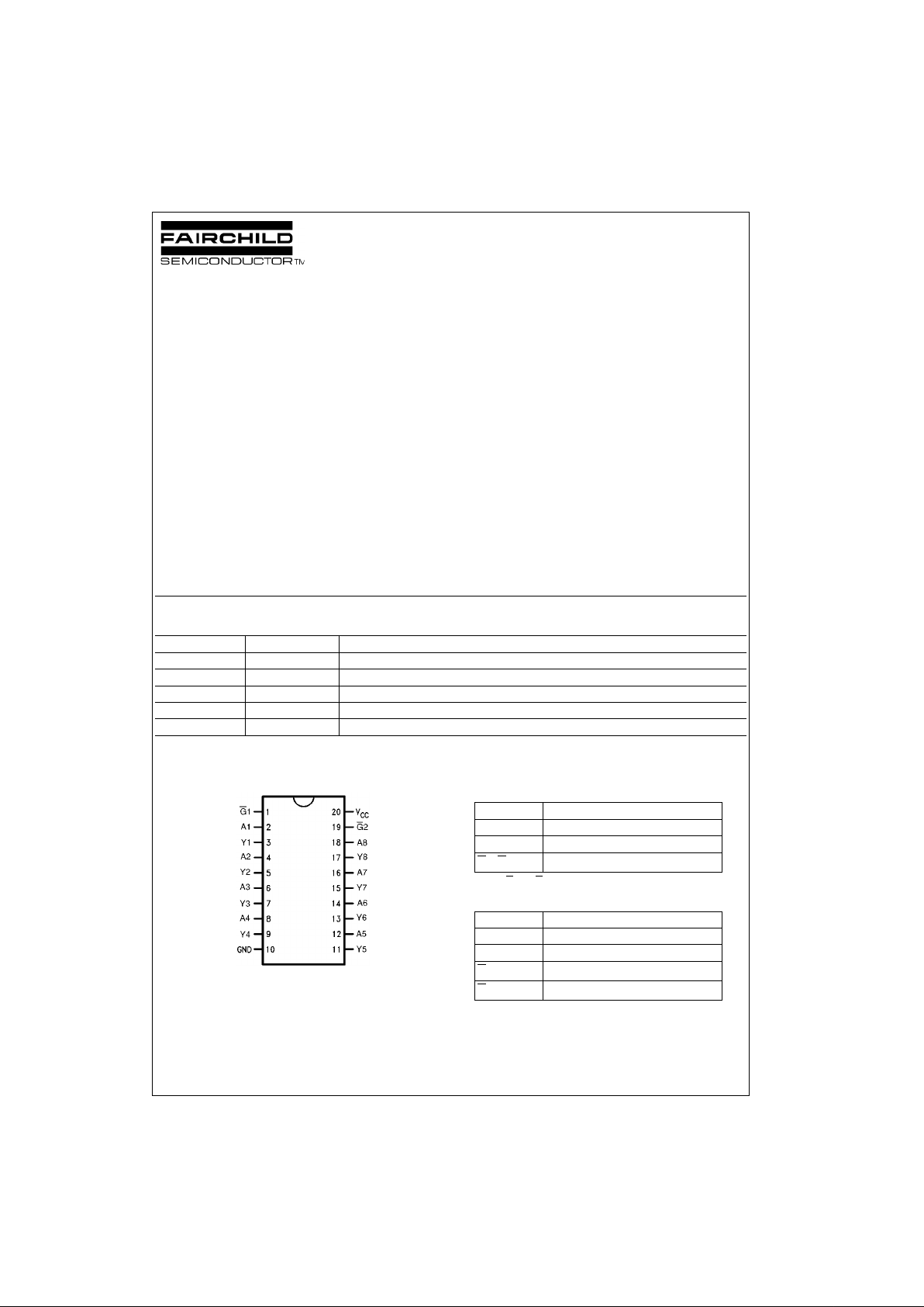
Connection Diagram Pin Descriptions
DM81LS95A and DM92LS 96 A
Note 1: Both G1 and G2 must be LOW for outpu ts t o be enabled.
DM81LS97A
Order Number Package Number Package Description
DM81LS95AWM M20B 20-Lead Small Outline Integrated Circuit (SOIC), JEDEC MS-013, 0.300 Wide
DM81LS95AN N20A 20-Lead Plastic Dual-In-Line Package (PDIP), JEDEC MS-001, 0.300 Wide
DM81LS96AWM M20B 20-Lead Small Outline Integrated Circuit (SOIC), JEDEC MS-013, 0.300 Wide
DM81LS96AN N20A 20-Lead Plastic Dual-In-Line Package (PDIP), JEDEC MS-001, 0.300 Wide
DM81LS97AN N20A 20-Lead Plastic Dual-In-Line Package (PDIP), JEDEC MS-001, 0.300 Wide
Pin Names Descriptions
A1–A8 Inputs
Y1–Y8 Outputs
G
1–G2
Active LOW Output Enables (Note 1)
Pin Names Descriptions
A1–A8 Inputs
Y1–Y8 Outputs
G
1
Active LOW Output Enable (Y1–Y4)
G
2
Active LOW Output Enable (Y5–Y8)
Page 2
www.fairchildsemi.com 2
DM81LS95A • DM81LS96A • DM81LS97A
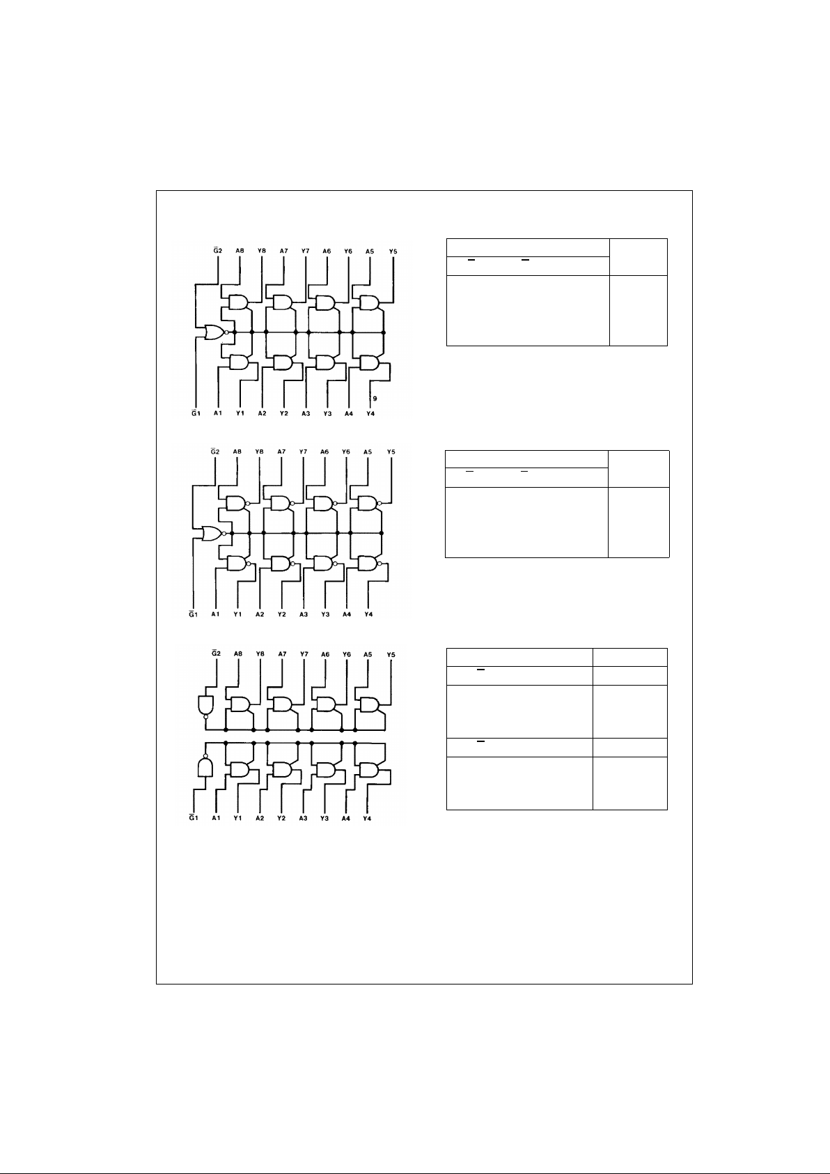
Logic Symbols
DM81LS95A
DM81LS96A
DM81LS97A
Tr uth Tables
DM81LS95A
DM81LS96A
DM81LS97A
Inputs Output
G
1G2A Y
H X X Hi-Z
X H X Hi-Z
LLHH
LLLL
Inputs Output
G
1G2A Y
H X X Hi-Z
X H X Hi-Z
LLH L
LLL H
Inputs Output
G
1 A1–A4 Y1–Y4
H X Hi-Z
LHH
LLL
G
2 A5–A6 Y5–Y8
H X Hi-Z
LHH
LLL
Page 3
3 www.fairchildsemi.com
DM81LS95A • DM81LS96A • DM81LS97A
Absolute Maximum Ratings(Note 2)
Note 2: The Absolute Maximum Ratings are those values beyond which
the safety of the device cannot be guaranteed. The device should not be
operated at these limits. The parametric values defined in the Electrical
Characteristics tables are not guaranteed at the absolute maximum ratings.
The Recommende d Operating Con ditions table will def ine the conditions
for actual device operation.
Recommended Operating Conditions
Supply Voltage 7V
Input Voltage 7V
Operating Free Air Temperature Range 0°C to +70°C
Storage Temperature Range −65°C to +150°C
Symbol Parameter Min Nom Max Units
V
CC
Supply Voltage 4.75 5 5.25 V
V
IH
HIGH Level Input Voltage 2 V
V
IL
LOW Level Input Voltage 0.8 V
I
OH
HIGH Level Output Current −5.2 mA
I
OL
LOW Level Output Current 24 mA
T
A
Free Air Operating Temperature 0 70 °C
Page 4

www.fairchildsemi.com 4
DM81LS95A • DM81LS96A • DM81LS97A
DC Electrical Characteristics DM81LS95A and DM81LS97A
over recommended operating free air temperature range (unless otherwise noted)
Note 3: All typicals are at VCC = 5V, TA = 25°C.
Note 4: Both G
inputs are at 2V.
Note 5: Both G
inputs are at 0.4V.
Note 6: Not more than one output should be shorted at a time, and the duration should not exceed one second.
AC Electrical Characteristics DM81LS95A and DM81LS97A
VCC = 5V, TA = 25°C
Note 7: CL = 5 pF.
Symbol Parameter Conditions Min
Typ
Max Units
(Note 3)
V
I
Input Clamp Voltage VCC = Min, II = −18 mA −1.5 V
V
OH
HIGH Level Output Voltage VCC = Min, IOH = Max
2.7 V
VIL = Max, VIH = Min
V
OL
LOW Level Output Voltage VCC = Min, IOL = Max
0.5
VIOL = Max, VIH = Min
IOL = 12 mA, VCC = Min 0.4
I
I
Input Current @ Max VCC = Max, VI = 7V
0.1 mA
Input Voltage
I
IH
HIGH Level Input Current VCC = Max, VI = 2.7V 20 µA
I
IL
LOW Level Input Current VCC = Max VI = 0.5V A (Note 4) −20
µA
VI = 0.4V A (Note 5) −50
G −50
I
OZH
Off-State Output Current VCC = Max, VO = 2.4V
20 µAwith HIGH Level Output VIH = Min, VIL = Max
Voltage Applied
I
OZL
Off-State Output Current VCC = Max, VO = 0.4V
−20 µAwith LOW Level Output VIH = Min, VIL = Max
Voltage Applied
I
OS
Short Circuit VCC = Max
−20 −100 mA
Output Current (Note 6)
I
CC
Supply Current VCC = Max (Note 4) 16 26 mA
Symbol Parameter
RL = 667 Ω
UnitsCL = 50 pF CL = 150 pF
Min Max Min Max
t
PLH
Propagation Delay Time
16 25 ns
LOW-to-HIGH Level Output
t
PHL
Propagation Delay Time
28 40 ns
HIGH-to-LOW Level Output
t
PZH
Output Enable Time
25 30 ns
to HIGH Level Output
t
PZL
Output Enable Time
30 42 ns
to LOW Level Output
t
PHZ
Output Disable Time
20 ns
from HIGH Level Output (Note 7)
t
PLZ
Output Disable Time
27 ns
from LOW Level Output (Note 7)
Page 5

5 www.fairchildsemi.com
DM81LS95A • DM81LS96A • DM81LS97A
DC Electrical Characteristics DM81LS96A
over recommended operating free air temperature range (unless otherwise noted)
Note 8: All typicals are at VCC = 5V, TA = 25°C.
Note 9: Both G
inputs are at 2V.
Note 10: Both G
inputs are at 0.4V.
Note 11: Not more than one output should be shorted at a t im e, and the duration should not exceed one secon d.
AC Electrical Characteristics DM81LS96A
VCC = 5V, TA = 25°C
Note 12: CL = 5 pF.
Symbol Parameter Conditions Min
Typ
Max Units
(Note 8)
V
I
Input Clamp Voltage VCC = Min, II = −18 mA −1.5 V
V
OH
HIGH Level Output Voltage VCC = Min, IOH = Max
2.7 V
VIL = Max, VIH = Min
V
OL
LOW Level Output Voltage VCC = Min, IOL = Max
0.5
VIOL = Max, VIH = Min
IOL = 12 mA, VCC = Min 0.4
I
I
Input Current @ Max VCC = Max, VI = 7V
0.1 mA
Input Voltage
I
IH
HIGH Level Input Current VCC = Max, VI = 2.7V 20 µA
I
IL
LOW Level Input Current VCC = Max VI = 0.5V A (Note 9) −20
µA
VI = 0.4V A (Note 10) −50
G
−50
I
OZH
Off-State Output Current VCC = Max, VO = 2.4V
20 µAwith HIGH Level Output VIH = Min, VIL = Max
Voltage Applied
I
OZL
Off-State Output Current VCC = Max, VO = 0.4V
−20 µAwith LOW Level Output VIH = Min, VIL = Max
Voltage Applied
I
OS
Short Circuit VCC = Max
−20 −100 mA
Output Current (Note 11)
I
CC
Supply Current VCC = Max (Note 10) 13 21 mA
Symbol Parameter
RL = 667 Ω
UnitsCL = 50 pF CL = 150 pF
Min Max Min Max
t
PLH
Propagation Delay Time
10 16 ns
LOW-to-HIGH Level Output
t
PHL
Propagation Delay Time
17 30 ns
HIGH-to-LOW Level Output
t
PZH
Output Enable Time
15 30 ns
to HIGH Level Output
t
PZL
Output Enable Time
35 45 ns
to LOW Level Output
t
PHZ
Output Disable Time
20 ns
from HIGH Level Output (Note 12)
t
PLZ
Output Disable Time
27 ns
from LOW Level Output (Note 12)
Page 6

www.fairchildsemi.com 6
DM81LS95A • DM81LS96A • DM81LS97A
Physical Dimensions inches (millimeters) unless otherwise noted
20-Lead Small Outline Integrated Circuit (SOIC), JEDEC MS-013, 0.300 Wide
Package Number M20B
Page 7

Physical Dimensions inches (millimeters) unless otherwise noted (Continued)
7 www.fairchildsemi.com
DM81LS95A • DM81LS96A • DM81LS97A 3-STATE Octal Buffer
Physical Dimensions inches (millimeters) unless otherwise noted (Continued)
20-Lead Plastic Dual-In-Line Package (PDIP), JEDEC MS-001, 0.300 Wide
Package Number N20A
Fairchild does not assume any responsibility for use of any circu itry described, no circuit patent license s are implied and
Fairchild reserves the right at any time without notice to change said circuitry and specifications.
LIFE SUPPORT POLICY
FAIRCHILD’S PRODUCTS ARE NOT AUTHORIZED FOR USE AS CRITICAL COMPONENTS IN LIFE SUPPORT
DEVICES OR SYSTEMS WITHOUT THE EXPRESS WRITTEN APPROVAL OF THE PRESIDENT OF FAIRCHILD
SEMICONDUCTOR CORPORATION. As used herein:
1. Life support de vices o r syst ems are dev ic es or syste ms
which, (a) are intended for surgical implant into the
body, or (b) support or sustain life, and (c) whose failure
to perform when properly used in accordance with
instructions for use provided i n the labe li ng, can be re asonably expected to result in a significant injury to the
user.
2. A critica l compo nent in any com ponen t of a life s uppor t
device or system whose failu re to perform can b e reasonably expected to c ause th e fa i lure of the li fe s upp or t
device or system, or to affect its safety or effectiveness.
www.fairchildsemi.com
 Loading...