

Page 1
DM74S280
9-Bit Parity Generator/Checker
DM74S280 9-Bit Parity Generator/Checker
August 1986
Revised May 2000
General Description
These universal, nine-bit parity generators/ch eckers utilize
Schottky-clamped TTL hi gh -pe rfo rm anc e ci rcu itry, and feature odd/even outputs to facilitate operation of either odd or
even parity applications. The word-length capability is ea sily expanded by cascading.
The DM74S280 can be used to upgr ade the perfor mance
of most systems utilizing the DM74180 parity generator/
checker. Although the DM74S280 is implemented without
expander inputs, the correspo nding funct ion is provi ded by
the availability of all input at pin 4, and no internal connection at pin 3. This perm its the DM 74S2 80 to be substitut ed
for the 180 in existing designs to produce an identical function, even if DM74S280’s are mixed with existing 180’s.
Input buffers are provided so that each input represents
only one normal 74S lo ad, and full fan-out to 10 normal
Series 74S loads is available fro m each of the outputs at
low logic levels. A fan-out to 20 normal Series 74S loads is
provided at high logic levels, to facilitate connection of
unused inputs to used inputs.
Features
■ Generates either odd or even parity for nine data lines
■ Cascadable for N-bits
■ Can be used to upgrade existing systems using MSI par-
ity circuits
■ Typical data-to-output delay—14 ns
Ordering Code:
Order Number Package Number Package Description
DM74S280M M14A 14-Lead Small Outline Integrated Circuit (SOIC), JEDEC MS-120, 0.150 Narrow
DM74S280N N14A 14-Lead Plastic Dual-In-Line Package (PDIP), JEDEC MS-001, 0.300 Wide
Devices also availab l e in Tape and Reel. Specify by appending th e s uffix let t er “X” to the ordering code.
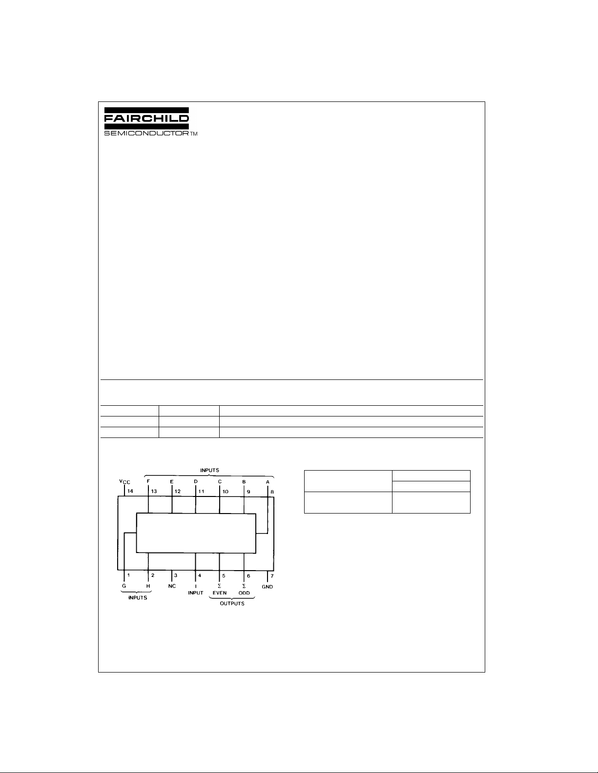
Connection Diagram Function Table
Number of Inputs Outputs
(A Thru I) that are HIGH ∑ Even ∑ Odd
0, 2, 4, 6, 8 H L
1, 3, 5, 7, 9 L H
© 2000 Fairchild Semiconductor Corporation DS006483 www.fairchildsemi.com
Page 2
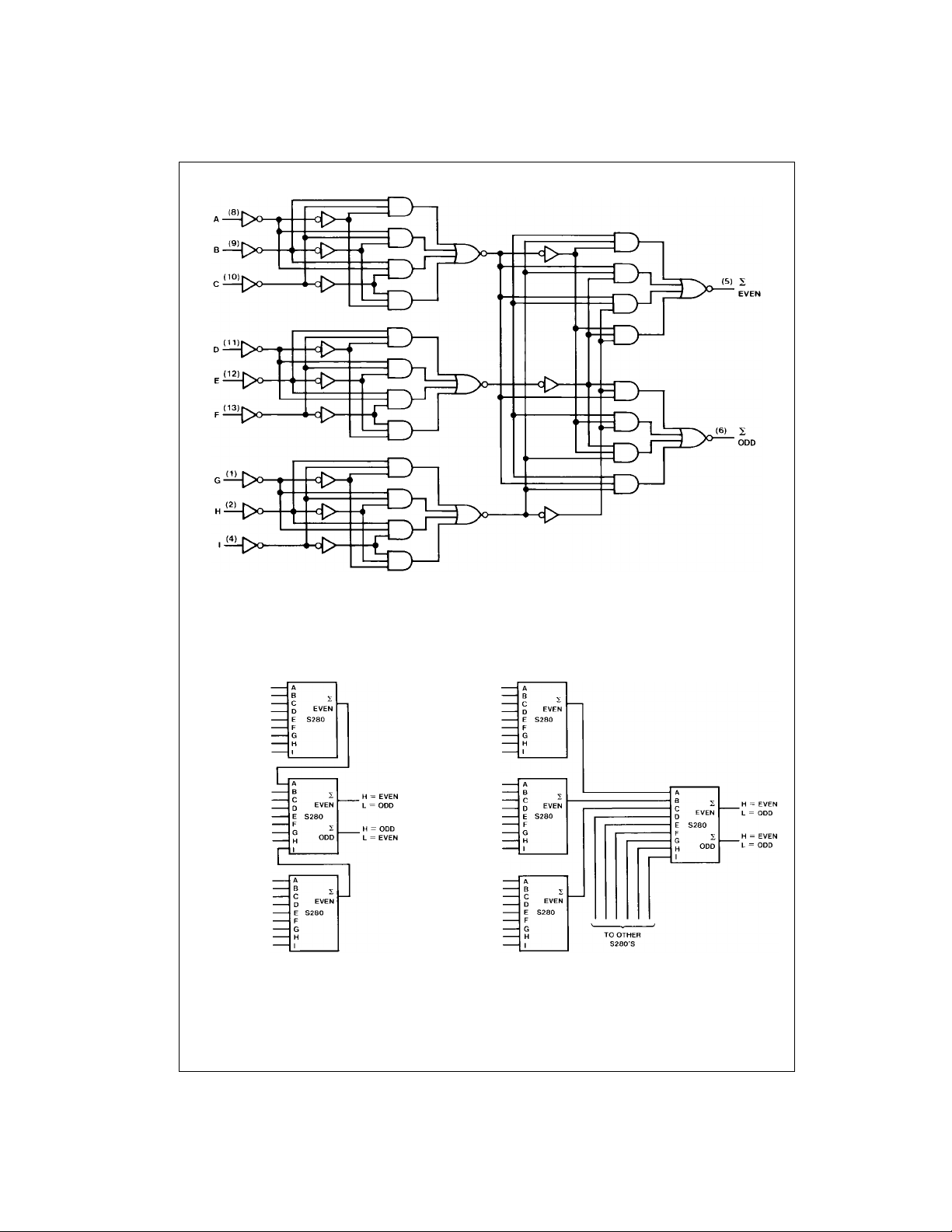
Logic Diagram
DM74S280
Typical Applications
Three DM74S280’s can be used to implement a 25-line
parity generator/checker. This arrangement will provide
parity in typically 25 ns. (See Figure 1.)
Longer word lengths can be implemented by cascading
DM74S280’s. As shown in Figure 2, parity can be gener-
ated for word lengths up to 81 bits in typically 25 ns.
FIGURE 1. 25-Line Parity/Generator Checker
www.fairchildsemi.com 2
FIGURE 2. 81-Line Parity/Generator Checker
Page 3

Absolute Maximum Ratings(Note 1)
Supply Voltage 7V
Input Voltage 5.5V
Operating Free Air Temperature Range 0°C to +70°C
Storage Temperature Range −65°C to +150°C
Note 1: The “Absolute Maximum Ratings” are those values bey ond whic h
the safety of the d evice cannot b e guaranteed . The device sh ould not be
operated at these limit s. The parametric values defi ned in the Electrical
Characteristics tab les are not guaranteed a t t he absolute maximum ratings.
The “Recomm ended O peratin g Cond itions ” table will defin e the condition s
for actual device operation.
Recommended Operating Conditions
Symbol Parameter Min Nom Max Units
V
CC
V
IH
V
IL
I
OH
I
OL
T
A
Supply Voltage 4.75 5 5 .25 V
HIGH Level Input Voltage 2 V
LOW Level In put Voltage 0.8 V
HIGH Level Output Current −1mA
LOW Level Output Current 20 mA
Free Air Operating Temperature 0 70 °C
Electrical Characteristics
over recommended operating free air temperature range (unless otherwise noted)
Symbol Parameter Conditions Min
V
I
V
OH
V
OL
I
I
I
IH
I
IL
I
OS
I
CC
Note 2: All typi c als are at VCC = 5V, TA = 25°C.
Note 3: Not more than one output sh ould be shorted at a time, and the duration should not exceed one s ec ond.
Note 4: I
Input Clamp Voltage VCC = Min, II=−18 mA −1.2 V
HIGH Level VCC = Min, IOH = Max
Output Voltage VIL = Max, VIH = Min
LOW Level VCC = Min, IOL =Max
Output Voltage VIH = Min, VIL = Max
Input Current @ Max Input Voltage VCC = Max, VI = 5.5V 1 mA
HIGH Level Input Current VCC = Max, VI = 2.7V 50 µA
LOW Level Input Current VCC = Max, VI = 0.5V −2mA
Short Circuit Output Current VCC = Max (Note 3) −40 −100 mA
Supply Current VCC Max (Note 4) 67 105 mA
is measured with all inputs grounded and all outputs OPEN.
CC
2.7 3.4 V
Typ
(Note 2)
Max Units
0.5 V
DM74S280
Switching Characteristics
at V
= 5V and T
CC
Symbol Parameter
t
PLH
t
PHL
t
PLH
t
PHL
= 25°C
A
Propagation Delay Time
LOW-to-HIGH Level Output
Propagation Delay Time
HIGH-to-LOW Level Output
Propagation Delay Time
LOW-to-HIGH Level Output
Propagation Delay Time
HIGH-to-LOW Level Output
RL = 280Ω RL = 280Ω
From (Input)
To (Output) Min Max Min Max
Data to ∑ Even 21 24 ns
Data to ∑ Even 18 21 ns
Data to ∑ Odd 21 24 ns
Data to ∑ Odd 18 21 ns
CL = 15 pF CL = 50 pF Units
3 www.fairchildsemi.com
Page 4

Physical Dimensions inches (millimeters) unless otherwise noted
DM74S280
14-Lead Small Outline Integrated Circuit (SOIC), JEDEC MS-120, 0.150 Narrow
Package Number M14A
www.fairchildsemi.com 4
Page 5

Physical Dimensions inches (millimeters) unless otherwise noted (Continued)
DM74S280 9-Bit Parity Generator/Checker
14-Lead Plastic Dual-In-Line Package (PDIP), JEDEC MS-001, 0.300 Wide
Fairchild does not assume any responsibility for use of any circuitry described , no circuit patent licenses are implied and
Fairchild reserves the right at any time without notice to change said circuitry and specifications.
LIFE SUPPORT POLICY
FAIRCHILD’S PRODUCTS ARE NOT AUTHORIZED FOR USE AS CRITICAL COMPONENTS IN LIFE SUPPORT
DEVICES OR SYSTEMS WITHOUT THE EXPRESS WRITTEN APPROVAL OF THE PRESIDENT OF FAIRCHILD
SEMICONDUCTOR CORPORATION. As used herein:
1. Life support devices or systems are dev ic es or syste ms
which, (a) are intended for surgical implant into the
body, or (b) support or sustain life, and (c) whose failure
to perform when properly used in accordance with
instructions for use provide d in the l abe ling, can be reasonably expected to result in a significant injury to the
user.
Package Number N14A
2. A critical compo nent in any com ponen t of a life s upp ort
device or system whose failure to perform can be reasonably expected to cause the failure of the life support
device or system, or to affect its safety or effectiveness.
www.fairchildsemi.com
5 www.fairchildsemi.com
 Loading...