

Page 1
1
www.clare.com
CPC7581
DS-CPC7581-R2
The CPC7581 is a monolithic solid state switch in a 16 pin
surface mount SOIC package. It provides the necessary
functions to replace a 2-Form-C electromechanical relay
on analog line cards found in Central Office, Access and
PBX equipment. The device contains solid state switches
for tip and ring line break and ring injection/ring return.
The CPC7581 requires only a +5V supply and offers
“break-before-make” or “make-before-break” switch operation using simple logic level input control. There are two
versions of the CPC7581, the CPC7581BA and the
CPC7581BB. The “BA” version has a protection SCR
which provides protection to the SLIC device and subsequent circuitry during fault conditions.
• Central office (CO)
• Digital Loop Carrier (DLC)
• PBX Systems
• Digitally Added Main Line (DAML)
• Hybrid Fiber Coax (HFC)
• Fiber in the Loop (FITL)
• Pair Gain System
• Channel Banks
• Small 16 pin surface mount SOIC package
• Monolithic IC reliability
• Low matched RDS
ON
• Eliminates the need for zero cross switching
• Flexible switch timing to transition from ringing mode
to idle/talk mode
• Clean, bounce free switching
• Tertiary Protection consisting of integrated current
limiting, thermal shutdown and SLIC protection
• 5V operation with power consumption <10mW
• Intelligent battery monitor
• Latched logic level inputs, no drive circuitry
• Pin to pin compatible to the Lucent 7581 family
Applications
Features
Description
Line Card Access Switch
Ordering Information
Part # Description
CPC7581BA 4 Pole with protection SCR
CPC7581BB 4 Pole without protection SCR
CPC7581BA-TR Tape & Reel Version
CPC7581BB-TR Tape & Reel Version
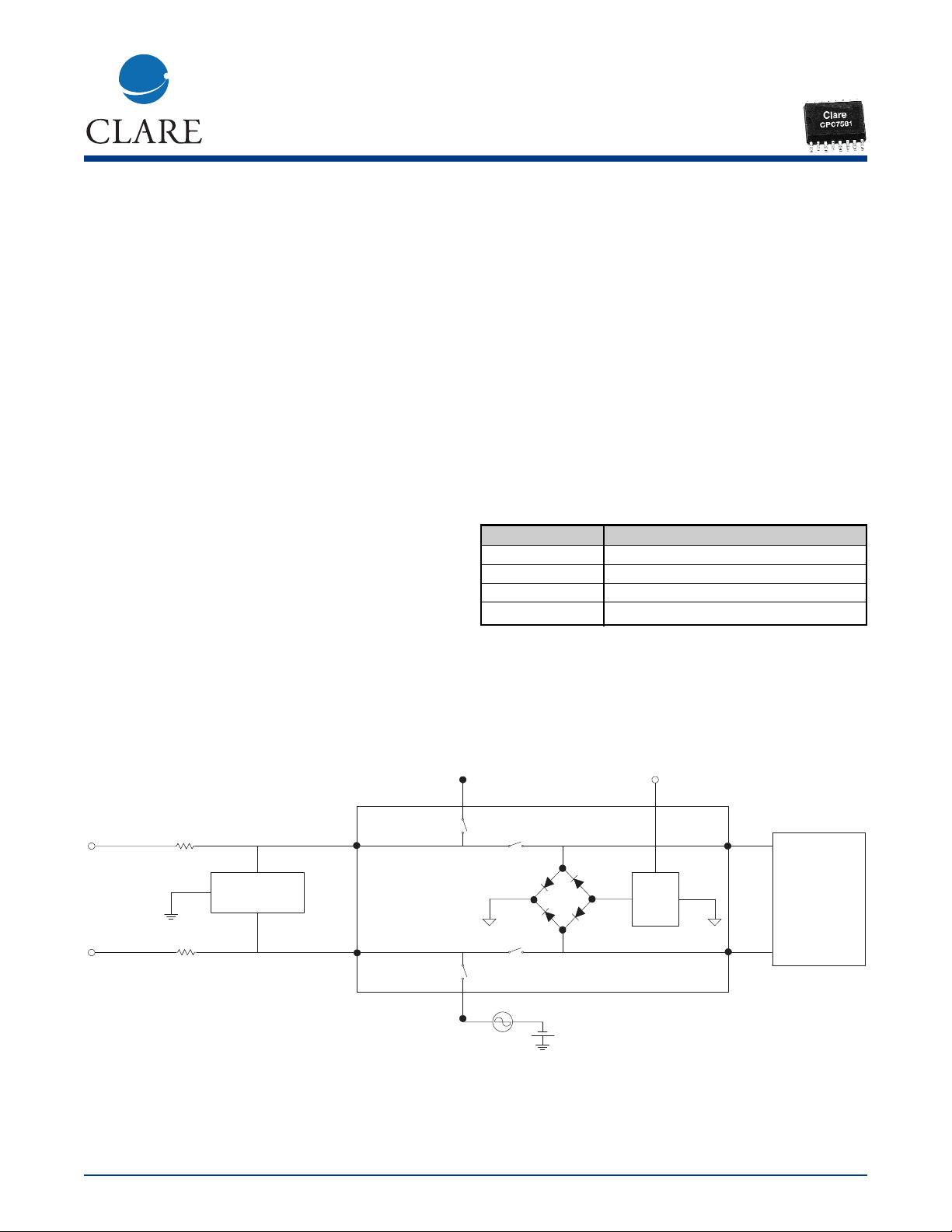
Block Diagram
TIP
Ring
R1
(6)
T
RING
SW3
Ringing
T
(3)
LINE
Secondary
Protection
R2
R
(14)
LINE
Return
SW4
Ringing
Access
R
RING
Break
Break
Ring Generator
(12)
SW1
SW2
-
+
CPC7581BA
Battery
SCR
and Trip
Circuit
V
BAT
Reference (16)
(2)
T
BAT
SLIC
R
(15)
BAT
Page 2
www.clare.com
CPC7581
Rev. 2
Absolute Maximum Ratings are stress ratings.
Functional operation of the device at these or any
other conditions beyond those indicated in the
operational sections of this data sheet is not
implied. Exposure of the device to the absolute
maximum ratings for extended period may degrade
the device and effect its reliability.
Absolute Maximum Ratings (@ 25˚ C)
2
Electrical Characteristics TA = -40oC to +85oC (unless otherwise specified)
Minimum and maximum values are production testing requirements. Typical values are characteristic of the device
and are the result of engineering evaluations. Typical values are provided for information purposes only.
1
V
BAT
is used only as a reference for internal protection circuitry.
If V
BAT
rises above -10V, the device will enter an all off state and will remain in the all off state until the battery voltage drops below -15V.
Power Supply Specifications
Supply Min Typ Max Unit
V
DD
+4.5 +5.0 +5.5 V
V
BAT
1
-19 - -72 V
ESD Rating (HBM)
1000V
Table 1. Break Switch, SW1 and SW2
PARAMETERS CONDITIONS SYMBOL MIN TYP MAX UNITS
Off-state Leakage Current:
+25˚C Vsw (differential)= -320V to Gnd Isw - 0.1 1 µA
Vsw (differential)= -60V to +260V
+85˚C Vsw (differential)= -330V to Gnd Isw - 0.3 1 µA
Vsw (differential)= -60V to +270V
-40˚C Vsw (differential)= -310V to Gnd Isw - 0.1 1 µA
Vsw (differential)= -60V to +250V
RDSON(SW1,SW2):
+25˚C T
LINE
= +/-10 mA, +/-40mA, T
BAT
= -2V ∆ V - 14.5 - Ω
+85˚C T
LINE
= +/-10 mA, +/-40mA, T
BAT
= -2V ∆ V - 20.5 28 Ω
-40˚C T
LINE
= +/-10 mA, +/-40mA, T
BAT
= -2V ∆ V - 10.5 - Ω
RDS
ON
Match Per ON-resistance Test Condition of Magnitude - 0.15 0.8 Ω
SW1, SW2 RONSW1-RONSW2
dc Current Limit: - - - - +25˚C Vsw (on) = +/- 10V Isw - 300 - mA
+85˚C Vsw (on) = +/- 10V Isw 80 160 - mA
-40˚C Vsw (on) = +/- 10V Isw - 400 425 mA
Dynamic Current Limit: Break switches in ON state, Ringing Isw - 2.5 - A
(t=<0.5µs) access switches OFF, Apply +/- 1000V
at 10/1000µs pulse, Appropriate
secondary protection in place.
Logic Input to Switch Output Isolation
+25˚C Vsw (T
LINE
, R
LINE
) = +/-320V Isw - 0.1 1 µA
Logic Inputs = Gnd
+85˚C Vsw (T
LINE
, R
LINE
) = +/-330V Isw - 0.3 1 µA
Logic Inputs = Gnd
-40˚C Vsw (T
LINE
, R
LINE
) = +/-310V Isw - 0.1 1 µA
Logic Inputs = Gnd
dv/dt Sensitivity
1
- - - 200 - V/µs
1
Applied voltage is 100 Vp-p square wave at 100Hz.
Parameter Min Max Units
Operating Temperature Range -40 +110 ˚C
Storage Temperature Range -40 +150 ˚C
Relative Humidity Range 5 95 %
Pin Soldering Temperature - +260 ˚C
(t=10 s max)
+5V Power Supply - 7 V
Battery Supply - -85 V
Logic Input Voltage - 7 V
Logic Input to Switch Output Isolation - 330 V
Switch Isolation (SW1, SW2, SW3) - 330 V
Switch Isolation (SW4) - 480 V
Page 3
CPC7581
www.clare.com
Rev. 2
3
Table 3. Ringing Access Switch, SW4
PARAMETERS CONDITIONS SYMBOL MIN TYP MAX UNITS
Off-state Leakage Current
+25˚C Vsw (differential)= -255V to +210V Isw - .05 1 µA
Vsw (differential)= +255V to -210V
+85˚C Vsw (differential)= -270V to +210V Isw - 0.1 1 µA
Vsw (differential)= +270V to -210V
-40˚C Vsw (differential)= -245V to +210V Isw - .05 1 µA
Vsw (differential)= +245V to -210V
ON Voltage Isw (on) = +/- 1mA - - 1.5 3 V
Ring Generator Current Vcc = 5V, INaccess = 0 I
R
- 0.1 0.25 mA
During Ring
Surge Current - - - - 2 A
Release Current - - - 300 - µA
RDS
ON
Isw (on) = +/-70mA, +/-80mA ∆ V - 8.5 12 Ω
Logic Input to Switch Output Isolation
+25˚C Vsw (R
RING
, R
LINE
) = +/-320V Isw - .05 1 µA
Logic Inputs = Gnd
+85˚C Vsw (R
RING
, R
LINE
) = +/-330V Isw - 0.1 1 µA
Logic Inputs = Gnd
-40˚C Vsw (R
RING
, R
LINE
) = +/-310V Isw - .05 1 µA
Logic Inputs = Gnd
Table 2. Ring Return Switch, SW3
PARAMETERS CONDITIONS SYMBOL MIN TYP MAX UNITS
Off-state Leakage Current
+25˚C Vsw (differential)= -320V to Gnd Isw - 0.1 1 µA
Vsw (differential)= -60V to +260V
+85˚C Vsw (differential)= -330V to Gnd Isw - 0.3 1 µA
Vsw (differential)= -60V to +270V
-40˚C Vsw (differential)= -310V to Gnd Isw - 0.1 1 µA
Vsw (differential)= -60V to +250V
dc Current Limit:
+25˚C Vsw (on) = +/- 10V Isw - 135 - mA
+85˚C Vsw (on) = +/- 10V Isw - 85 - mA
-40˚C Vsw (on) = +/- 10V Isw - 210 - mA
Dynamic Current Limit: Break switches in ON state, Ringing Isw - 2.5 - A
(t=<0.5µs) access switches OFF, Apply +/- 1000V
at 10/1000ms pulse, Appropriate
secondary protection in place.
RDS
ON
+25˚C Isw (on) = +/-0mA, +/-10mA ∆ V-60-Ω
+85˚C Isw (on) = +/-0mA, +/-10mA ∆ V - 85 100 Ω
-40˚C Isw (on) = +/-0mA, +/-10mA ∆ V-45-Ω
Logic Input to Switch Output Isolation
+25˚C Vsw (T
RING
, T
LINE
) = +/-320V Isw - 0.1 1 µA
Logic Inputs = Gnd
+85˚C Vsw (T
RING
, T
LINE
) = +/-330V Isw - 0.3 1 µA
Logic Inputs = Gnd
-40˚C Vsw (T
RING
, T
LINE
) = +/-310V Isw - 0.1 1 µA
Logic Inputs = Gnd
Page 4
www.clare.com
4
CPC7581
Rev. 2
Table 4. Additional Electrical Characteristics
PARAMETERS CONDITIONS SYMBOL MIN TYP MAX UNITS
Digital Input Characteristics
Input Low Voltage - - - 2.2 1.5 V
Input High Voltage - - 3.5 2.2 - V
Input Leakage Current (High) V
DD
= 5.5V, V
BAT
= -75V, I
log
- 0.1 1 µA
V
log
= 5V
Input Leakage Current (Low) V
DD
= 5.5V, V
BAT
= -75V, I
log
- 0.1 1 µA
V
log
= 0V
Power Requirements
Power Dissipation VDD= 5V, V
BAT
= -48V,
Idle/Talk State or All Off State IDD, I
BAT
- 5.5 7.5 mW
Ringing State or Access State I
DD
- 6.5 10 mW
VDDCurrent VDD= 5V,
Idle/Talk State or All Off State I
DD
- 1.1 1.5 mA
Ringing State or Access State I
DD
- 1.3 1.9 mA
V
BAT
Current V
BAT
= -48V,
Idle/Talk State or All Off State I
BAT
- 0.1 10 µA
Ringing State or Access State I
BAT
- 0.1 10 µA
Temperature Shutdown Requirements
1
Shutdown Activation Temperature - - 110 125 150 ˚C
Shutdown Circuit Hysteresis - - 10 - 25 ˚C
1
Temperature shutdown flag (TSD) will be high during normal operation and low during temperature shutdown state.
Page 5

CPC7581
www.clare.com 5
Rev. 2
Table 5. Make-Before-Break Operation (Ringing to Idle/Talk Transition)
Ring Ring
Break Return Access
Switches Switch Switch
Input TSD State Timing 1 & 2 3 4
5V 5V/Float Ringing - Open Closed Closed
0V 5V/Float Make-before-break SW4 waiting for next zero current Closed Open Closed
crossing to turn off. Maximum
time is half of ringing. In this
transition state, current that is
limited to the dc break switch
current limit value will be sourced
from the ring node of the SLIC
0V 5V/Float Idle / Talk Zero cross current has occurred Closed Open Open
Table 6. Break-Before-Make Operation (Ringing to Idle/Talk Transition)
Ring Ring
Break Return Access
Switches Switch Switch
Input TSD State Timing 1 & 2 3 4
5V 5V/Float Ringing - Open Closed Closed
5V 0V All Off Hold this state for <=25ms. Open Open Closed
SW4 waiting for zero current to
turn off.
0V 0V All/Off Zero current has occurred Open Open Open
SW4 has opened
0V 5V/Float Idle/Talk Release Break Switches Closed Open Open
Page 6

www.clare.com
6
CPC7581
Rev. 2
Table 8. Truth Table
Input TSD Tip Break Ring Ringing Ring State
Switch Break Return Switch
Switch Switch
0V 5V/Float
1
On On Off Off Idle/Talk
5V 5V/Float
1
Off Off On On Ringing
Don’t 0V
2
Off Off Off Off All Off
Care
1
Thermal shutdown mechanism is active with TSD floating or equal to 5V and cannot be disabled.
2
Forcing TSD to ground overrides the logic input pins and forces an all off state.
Table 7. Electrical Specifications, Protection Circuitry
PARAMETER CONDITIONS SYMBOL MIN TYP MAX UNITS
Parameters Related to Diodes
(in Diode Bridge)
Voltage Drop @ Continuous Apply +/-dc current limit of break Forward - 2.1 3 V
Current (50/60 Hz) switches Voltage
Voltage Drop @ Surge Apply +/-dynamic current limit of Forward - 5 - V
Current break switches Voltage
Parameters Related to
Protection SCR
1
Surge Current - - - - * A
Trigger Current (+25˚C) - I
TRIG
-60 - mA
Hold Current (+25˚C) - I
HOLD
- 100 - mA
Trigger Current (+85˚C) - I
TRIG
-35 - mA
Hold Current (+85˚C) I
HOLD
60 70 - mA
Gate Trigger Voltage Trigger Current - V
BAT
- 4 - V
BAT
- 2 V
Reverse Leakage Current V
BAT
- - - 1.0 µA
ON State Voltage
1
0.5A t = 0.5 ms V
on
--3 - V
2.0A t = 0.5 ms - - -5 - V
1
Only for the CPC7581BA.
* Passes GR1089 & ITU-T K.20 with appropriate secondary protection in place.
Page 7

CPC7581
www.clare.com
7
Rev. 2
Package Pinout
* Only the CPC7581BA contains the protection SCR.
CPC7581
1
2
3
4
16
15
14
13
5
6
7
8
T
BAT
12
11
10
9
SW3
SW1
SW4
SW2
Temperature
Shutdown
F
GND
T
LINE
T
RING
V
DD
TSD
D
GND
V
BAT
R
BAT
R
LINE
R
RING
LATCH
INPUT
NC
NC
NC
SCR
and
TRIP
CKT
Pin Name Function
1F
GND
Fault ground
2T
BAT
Connect to TIP on SLIC side
3T
LINE
Connect to TIP on line side
4 NC No Connect
5 NC No Connect
6T
RING
Connect to return ground for ringing
generator
7VDD+ 5V Supply
8
TSD
Temperature shutdown pin. Can be
used as a logic level input or output.
See Tables 5, 6 and 8 for more
details. As an output, will read
+5V when device is in its operational
mode and 0V in the thermal
shutdown mode.
9D
GND
Digital Ground
10 INPUT Logic level input switch control
11 LATCH Data latch control, active high,
transparent low
12 R
RING
Connect to ringing generator
13 NC No Connect
14 R
LINE
Connect to RING on line side
15 R
BAT
Connect to RING on SLIC side
16 V
BAT
Battery voltage. Reference for
protection circuit
Page 8

www.clare.com
8
CPC7581
Rev. 2
Functional Description
Introduction
The CPC7581 has three states:
• Idle/talk state (line break switches SW1, and SW2
closed, ringing switches SW3, SW4 open)
• Ringing state (line break switches SW1, and SW2
open, ringing switches SW3, SW4 closed)
• All Off state (line break switches SW1, and SW2
open, ringing switches SW3, SW4 open)
The CPC7581 offers break-before-make and makebefore-break switching with simple logic level input control. Solid state switch construction means no impulse
noise is generated when switching during ring cadence
or ring trip, thus eliminating the need for external “zero
cross” switching circuitry. State control is via logic level
input so no additional driver circuitry is required. The line
break switches SW1 and SW2 are linear switches that
have exceptionally low RDSON and excellent matching
characteristics. The ringing access switch SW4 has a
breakdown voltage rating of >480V which is sufficiently
high, with proper protection, to prevent breakdown in the
presence of a transient fault condition.
Integrated into the CPC7581 is a diode bridge/SCR
clamping circuit, current limiting and thermal shutdown
mechanism to provide protection to the SLIC device
during a fault condition. Positive and negative surges
are reduced by the current limiting circuitry and steered
to ground via diodes and the integrated SCR. Power
cross transients are also reduced by the current limiting
and thermal shutdown circuits. Please note that only
the CPC7581BA has the integrated protection SCR.
To protect the CPC7581 from an overvoltage fault condition, use of a secondary protector is required. The
secondary protector must limit the voltage seen at the
tip and ring terminals to a level below the max breakdown voltage of the switches. To minimize the stress on
the solid-state contacts, use of a foldback or crowbar
type secondary protector is recommended. With proper
selection of the secondary protector, a line card using
the CPC7581 will meet all relevant ITU, LSSGR, FCC
or UL protection requirements.
The CPC7581 operates from a +5V supply only. This
gives the device extremely low idle and active power dissipation and allows use with virtually any range of battery
voltage. A battery voltage is also used by the CPC7581
as a reference for the integrated protection circuit. In the
event of a loss of battery voltage, the CPC7581 will enter
an “all off” state.
Switch Timing
The CPC7581 provides, when switching from the ringing
state to the idle/talk state, the ability to control the timing
when the ringing access switches SW3 and SW4 are
released relative to the state of the line break switches
SW1 and SW2 using simple logic level input. This is
referred to a “make before break” or “break before make”
operation. When the line break switch contacts (SW1,
SW2) are closed (or made) before the ringing access
switch contact (SW3, SW4) is opened (or broken), this is
referred to a “make-before-break” operation. “Breakbefore-make” operation occurs when the ringing access
contact (SW3, SW4) is opened (broken) before the line
break switch contacts (SW1, SW2) are closed (made).
With the CPC7581 the “make before break” and “break
before make” operations can easily be selected by applying logic level inputs to pin 10 of the device.
The logic sequences for either mode of operation are
given in Tables 5 and 6. Logic states and explanations
are given in Table 8.
Ring Access Switch Zero Cross Current Turn Off
After the application of a logic input to turn SW4 off, the
ring access switch is designed to delay the change in
state until the next zero crossing. Once on, the switch
requires a zero current cross to turn off and therefore
should not be used to switch a pure DC signal. The
switch will remain in the on state no matter what logic
input until the next zero crossing. For proper operation,
pin 12 (R
Ring
) should be connected using proper impedance to a ring generator or other AC source. These
switching characteristics will reduce and possibly eliminate overall system impulse noise normally associated
with ringing access switches. The attributes of ringing
access switch SW4 may make it possible to eliminate
the need for a zero cross switching scheme. A minimum
impedance of 300Ω in series with the ring generator is
recommended.
Power Supplies
Both a +5V supply and battery voltage are connected
to the CPC7581. CPC7581 switch state control is powered exclusively by the +5V supply. As a result, the
CPC7581 exhibits extremely low power dissipation during both active and idle states.
The battery voltage is not used for switch control but
rather as a reference by the integrated secondary protection circuitry. The integrated SCR is designed to trigger when pin 2 (T
BAT
) or pin 15 (R
BAT
) drops 2 to 4V
below the battery. This trigger prevents a fault induced
overvoltage event at the T
BAT
or R
BAT
nodes.
Page 9

CPC7581
www.clare.com
9
Rev. 2
Battery Voltage Monitor
The CPC7581 also uses the voltage reference to monitor battery voltage. If battery voltage is lost, the CPC7581
will immediately enter the “all off” state and remain in this
state until the battery voltage is restored. The device will
also enter the “all off” state if the battery voltage rises
above –10V and will remain there until the battery voltage drops below –15V. This battery monitor feature
draws a small current from the battery (< 1µA typ.) and
will add slightly to the device’s overall power dissipation.
Protection
Diode Bridge/SCR
The CPC7581 uses a combination of current limited
break switches, a diode bridge/SCR clamping circuit
and a thermal shutdown mechanism to protect the SLIC
device or other associated circuitry from damage during
line transient events such as lightning. During a positive
transient condition, the fault current is conducted
through the diode bridge and to ground. Voltage is
clamped to the diode drop above ground. During a negative transient of two to four volts more negative than
the battery, the SCR conducts and faults are shunted to
ground via the SCR and diode bridge.
Also, in order for the SCR to crowbar or foldback, the on
voltage (see Table 7) of the SCR must be less negative
than the battery reference voltage. If the battery voltage
is less negative the SCR on voltage, the SCR will not
crowbar, however it will conduct fault currents to ground.
For power induction or power cross fault conditions, the
positive cycle of the transient is clamped to the diode
drop above ground and the fault current directed to
ground. The negative cycle of the transient will cause
the SCR to conduct when the voltage exceeds the battery reference voltage by two to four volts, steering the
current to ground.
Current Limiting function
If a lightning strike transient occurs when the device in
the talk/idle state, the current is passed along the line to
the integrated protection circuitry and limited by the
dynamic current limit response of break switches SW1
and SW2. When a 1000V 10x1000 pulse (LSSGR lightning) is applied to the line though a properly clamped
external protector, the current seen at pins 2 (T
BAT
) and
pin 15 (R
BAT
) will be a pulse with a typical magnitude
and duration of 2.5A and < 0.5ms.
If a power cross fault occurs with device in the talk/idle
state, the current is passed though the break switches
SW1 and SW2 on to the integrated protection circuit
and is limited by the dynamic DC current limit response
of the two break switches. The DC current limit, specified
over temperature, is between 80mA and 425mA and the
circuitry has a negative temperature coefficient. As a
result, if the device is subjected to extended heating due
to power cross fault, the measured current at pin 2 (T
BAT
)
and pin 15 (R
BAT
) will decrease as the device temperature increases. If the device temperature rises sufficiently, the temperature shutdown mechanism will activate
and the device will default to the “all off” state.
Temperature Shutdown
The thermal shutdown mechanism will activate when
the device temperature reaches a minimum of 110°C
placing the device in the “all off” state regardless of logic
input. During this thermal shutdown mode, pin 8 (TSD)
will read 0V. Normal output of TSD is +V
DD
If presented with a short duration transient such as a
lightning event, the thermal shutdown feature will not
typically activate. But in an extended power cross transient, the device temperature will rise and the thermal
shutdown will activate forcing the switches to an “all off”
state. At this point the current measured at pin 2 (T
BAT
)
and pin 15 (R
BAT
) will drop to zero. Once the device
enters thermal shutdown it will remain in the “all off”
state until the temperature of the device drops below
the activation level of the thermal shutdown circuit. This
will return the device to the state prior to thermal shutdown. If the transient has not passed, current will flow
at the value allowed by the dynamic DC current limiting
of the switches and heating will begin again, reactivating the thermal shutdown mechanism. This cycle of
entering and exiting the thermal shutdown mode will
continue as long as the fault condition persists. If the
magnitude of the fault condition is great enough, the
external secondary protector could activate and shunt
all current to ground.
External Protection Elements
The CPC7581 requires only one overvoltage secondary
protector on the loop side of the device. The integrated
protection feature described above negates the need
for protection on the line side. The purpose of the secondary protector is to limit voltage transients to levels
that do not exceed the breakdown voltage or input-output isolation barrier of the CPC7581. A foldback or
crowbar type protector is recommended to minimize
stresses on the device.
Consult Clare’s application note, AN-100, “Designing
Surge and Power Fault Protection Circuits for Solid
State Subscriber Line Interfaces” for equations related
to the specifications of external secondary protectors,
fused resistors and PTCs.
Page 10

www.clare.com
10
CPC7581
Rev. 2
Data Latch
The CPC7581 has an integrated data latch. The latch
operation is controlled by logic level input pin 11
(LATCH). The data input of the latch is pin 10 (INPUT)
and of the device while the output of the data latch is an
internal node used for state control. When LATCH control pin is at logic 0, the data latch is transparent and data
control signals flow directly through to state control. A
change in input will be reflected in a change is switch
state. When LATCH control pin is at logic 1, the data
latch is now active and a change in input control will not
affect switch state. The switches will remain in the position they were in when the LATCH changed from logic 0
to logic 1 and will not respond to changes in input as long
as the latch is at logic 1. In addition, TSD input is not tied
to the data latch. Therefore, TSD is not affected by the
LATCH input and TSD input will override state control via
pin 10 (IN
RING
) and the LATCH.
Page 11

CPC7581
www.clare.com
11
Rev. 2
Dimensions
mm
(Inches)
MECHANICAL DIMENSIONS
7.40 MIN / 7.60 MAX
(.291 MIN / .299 MAX)
0.23 MIN / 0.32 MAX
(.0091 MIN / .0125 MAX)
1.27
(.050)
2.44 MIN / 2.64 MAX
(.096 MIN / .104 MAX)
0.51 MIN / 1.01 MAX
(.020 MIN / .040 MAX)
10.11 MIN / 10.51 MAX
(.398 MIN / .414 MAX)
0.36 MIN / 0.46 MAX
(.014 MIN / .018 MAX)
10.11 MIN / 10.31 MAX
(.398 MIN / .406 MAX)
16 Pin SOIC (JEDEC Package)
PC Board Pattern
(Top View)
1.193
(.047)
9.728 ± .051
(.383 ± .002)
.787
(.031)
1.270
(.050)
Page 12

CLARE LOCATIONS
Clare Headquarters
78 Cherry Hill Drive
Beverly, MA 01915
Tel: 1-978-524-6700
Fax: 1-978-524-4900
Toll Free: 1-800-27-CLARE
Clare Micronix Division
145 Columbia
Aliso Viejo, CA 92656-1490
Tel: 1-949-831-4622
Fax: 1-949-831-4628
Clare Switch division
4315 N. Earth City Expressway
Earth City, MO 63045
Tel: 1-314-770-1832
Fax: 1-314-770-1812
SALES OFFICES
AMERICAS
Americas Headquarters
Clare
78 Cherry Hill Drive
Beverly, MA 01915
Tel: 1-978-524-6700
Fax: 1-978-524-4900
Toll Free: 1-800-27-CLARE
Eastern Region
Clare
603 Apache Court
Mahwah, NJ 07430
Tel: 1-201-236-0101
Fax: 1-201-236-8685
Toll Free: 1-800-27-CLARE
Central Region
Clare Canada Ltd.
3425 Harvester Road, Suite 202
Burlington, Ontario L7N 3N1
Tel: 1-905-333-9066
Fax: 1-905-333-1824
Western Region
Clare
1852 West 11th Street, #348
Tracy, CA 95376
Tel: 1-209-832-4367
Fax: 1-209-832-4732
Toll Free: 1-800-27-CLARE
Canada
Clare Canada Ltd.
3425 Harvester Road, Suite 202
Burlington, Ontario L7N 3N1
Tel: 1-905-333-9066
Fax: 1-905-333-1824
EUROPE
European Headquarters
Clare, Inc.
Bampslaan 17
B-3500 Hasselt (Belgium)
Tel: 32-11-300868
Fax: 32-11-300890
France
Clare France Sales
Lead Rep
99 route de Versailles
91160 Champlan
France
Tel: 33 1 69 79 93 50
Fax: 33 1 69 79 93 59
Germany
Clare Germany Sales
ActiveComp Electronic GmbH
Mitterstrasse 12
85077 Manching
Germany
Tel: 49 8459 3214 10
Fax: 49 8459 3214 29
Italy
C.L.A.R.E.s.a.s.
Via C. Colombo 10/A
I-20066 Melzo (Milano)
Tel: 39-02-95737160
Fax: 39-02-95738829
Sweden
Clare Sales
Comptronic AB
Box 167
S-16329 Spånga
Tel: 46-862-10370
Fax: 46-862-10371
United Kingdom
Clare UK Sales
Marco Polo House
Cook Way
Bindon Road
Taunton
UK-Somerset TA2 6BG
Tel: 44-1-823 352541
Fax: 44-1-823 352797
ASIA/PACIFIC
Asian Headquarters
Clare
Room N1016, Chia-Hsin,
Bldg II, 10F, No. 96, Sec. 2
Chung Shan North Road
Taipei, Taiwan R.O.C.
Tel: 886-2-2523-6368
Fax: 886-2-2523-6369
http://www.clare.com
Worldwide Sales Offices
Specification: DS-CPC7581-R2
©Copyright 2000, Clare, Inc.
All rights reserved. Printed in USA.
7/16/01
Clare cannot assume responsibility for use of any circuitry other
than circuitry entirely embodied in this Clare product. No circuit
patent licenses nor indemnity are expressed or implied. Clare
reserves the right to change the specification and circuitry, without notice at any time. The products described in this document
are not intended for use in medical implantation or other direct life
support applications where malfunction may result in direct physical harm, injury or death to a person.
 Loading...