

Page 1
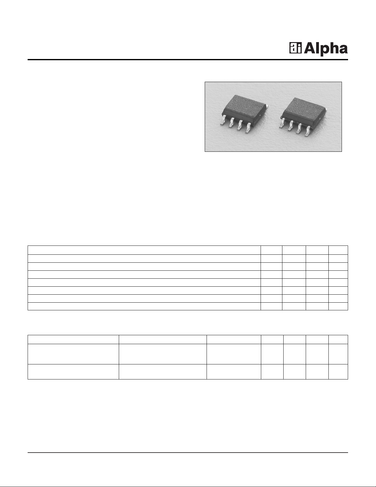
Alpha Industries, Inc. [781] 935-5150 • Fax [617] 824-4579 • Email sales@alphaind.com • www.alphaind.com 1
Specifications subject to change without notice. 6/01A
HIP3™ Variable Attenuator
0.80–1.00 GHz
Features
■ +40 dBm IP3 Typical
■ Low Loss 1 dB Typical
■ Attenuation 30 dB Typical
■ Good VSWR <1.5:1 Typical
■ Low Phase Shift
AV111-12
Description
The AV111-12 is a current controlled variable attenuator
from Alpha’s series of HIP3™ components. It is designed
to meet the wide dynamic range required in spread
spectrum wireless base station applications. A monolithic
quadrature hybrid is teamed with a silicon PIN diode pair
in a plastic surface mount package reducing size and
assuring consistency from part to part.
Parameter Min. Typ. Max. Unit
Frequency 0.80 1.0 GHz
Insertion Loss (0 mA Control Current) 1.0 1.5 dB
Attenuation @ 1.2 mA Control Current (900 MHz) 17.5 21.5 dB
VSWR All Ports 1.5 1.8
Input 3rd Order Intercept +37 +40 dBm
Relative Phase Shift Up to 20 dB Attenuation
1
7 10 Deg.
Group Delay 0.4 0.9 ns
Electrical Specifications at 25°C
Parameter
2
Condition Frequency Min. Typ. Max. Unit
Switching Characteristics
3
Rise, Fall (10/90% or 90/10% RF) 5 µs
On, Off (50% CTL to 90/10% RF) 8 µs
Video Feedthru (Peak) 5 mV
Maximum Input Power for <1 dB +15 dBm
Attenuation Variation
Operating Characteristics at 25°C (0, +5 V)
1. When built with external components as shown in the Pin Out diagram.
2. All measurements made in a 50 Ω system, unless otherwise specified.
3. 0–4 mA square wave total control current.
SOIC-8
SOIC-8
Page 2
2 Alpha Industries, Inc. [781] 935-5150 • Fax [617] 824-4579 • Email sales@alphaind.com • www.alphaind.com
Specifications subject to change without notice. 6/01A
HIP3™ Variable Attenuator 0.80–1.00 GHz AV111-12
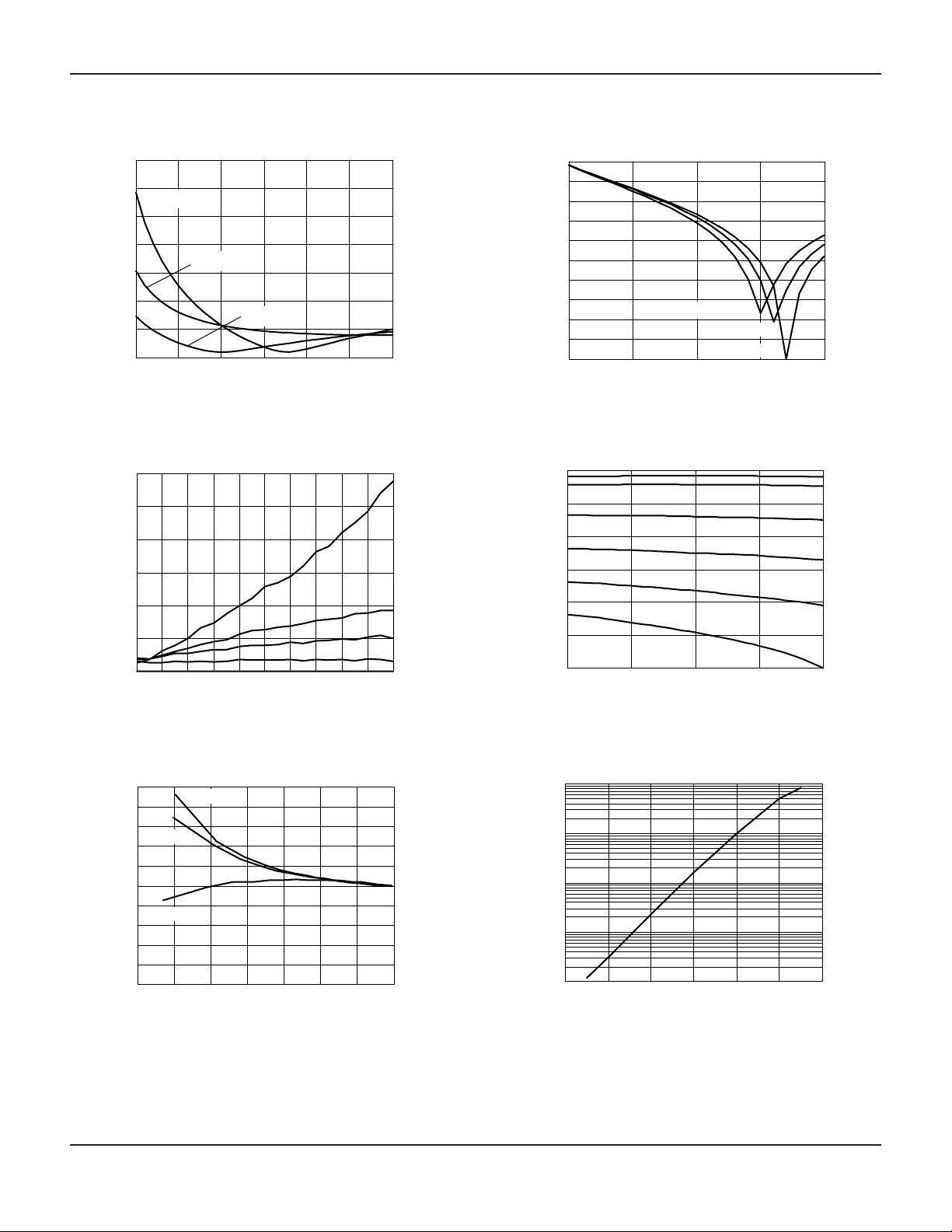
VSWR
Input/Output VSWR vs. Current
Current (mA)
1.00
1.10
1.20
1.30
1.40
1.50
1.60
1.70
0.50 1.0 1.5 2.0 2.5 3.0
800 MHz
900 MHz
1 GHz
Attenuation (dB)
0 0.5 1.0 1.5 2.0
Attenuation vs. Current
-50
-40
-30
-20
-10
-45
-35
-25
-15
-5
0
Current (mA)
1000 MHz
900 MHz
800 MHz
Relative Phase Shift (Degrees)
Relative Phase vs. Frequency
0
4
8
12
16
20
24
Frequency (GHz)
0.80 0.84 0.88 0.92 0.96 1.00
0.5 mA
0 mA
1.0 mA
1.2 mA
1.4 mA
Attenuation (dB)
0.80 0.85 0.90 0.95 1.00
Attenuation vs. Frequency
-30
-25
-20
-15
-10
-5
0
Frequency (GHz)
0 mA
0.1 mA
0.5 mA
0.9 mA
1.2 mA
1.4 mA
Relative Phase vs. Attenuation
-25
-20
-15
-10
-5
0
5
10
15
20
25
Attenuation (dB)
Relative Phase Shift (Degrees)
-35 -30 -25 -20 -15 -10 -5 0
800 MHz
900 MHz
1000 MHz
Current (mA)
400 600 700 900500 800 1000
Typical PIN Diode Current vs. Voltage
0.01
0.1
1
100
10
Voltage (V)
Typical Performance Data
Page 3

HIP3™ Variable Attenuator 0.80–1.00 GHz AV111-12
Alpha Industries, Inc. [781] 935-5150 • Fax [617] 824-4579 • Email sales@alphaind.com • www.alphaind.com 3
Specifications subject to change without notice. 6/01A
Characteristic Value
RF Input Power 0.5 W CW, 4 W @ 12.5%
Duty Cycle
Control Current 50 mA per Diode
Operating Temperature -65 to +125°C
Storage Temperature -65 to +125°C
Maximum Reverse Diode Voltage -100 V
Electrostatic Discharge +125 V
Absolute Maximum Ratings
Note: Operating this device above any of these parameters may cause
irreversible damage.
Recommended Board Layout
RF In/OutRF In/Out
20 mil Diameter
Ground Via
Pin 1
22 nH
Bias Input
120 pF
0.018
680 Ω
SK38531
AV10✳-12
SOIC-8
0.049
(1.24 mm)
0.016
(0.41 mm)
0.016 MAX.
(0.41 mm) x
45˚ CHAMFER
PIN 1
0.197 (5.00 mm)
0.189 (4.80 mm)
0.068
(1.73 mm) MAX.
0.010 (0.25 mm)
0.004 (0.10 mm)
0.010 (0.25 mm)
0.007 (0.17 mm)
0.158 (4.00 mm)
0.150 (3.80 mm)
8˚
MAX.
0.020 (0.51 mm) MAX.
0.244 (6.20 mm)
0.228 (5.80 mm)
0.050 (1.27 mm) BSC
PIN 8
PIN 1
INDICATOR
123 4
CONTROL
CURRENT
GND
220 pF
RF In
GND
680 Ω
876 5
GND
220 pF
100 nH 100 nH
RF Out
CONTROL
CURRENT
GND
Pin Out
CONTROL
CURRENT
CONTROL
CURRENT
RF OUT
RF IN
Connection Diagram
Material is 10 mil FR4.
 Loading...