

Page 1

INTEGRATED CIRCUITS
AU5790
Single wire CAN transceiver
Product data
Supersedes data of 2001 Jan 31
IC18 Data Handbook
2001 May 18
Page 2

Philips Semiconductors Product data
AU5790Single wire CAN transceiver
FEATURES
•Supports in-vehicle class B multiplexing via a single bus line with
ground return
•33 kbps CAN bus speed with loading as per J2411
•83 kbps high-speed transmission mode
•Low RFI due to output waveshaping
•Direct battery operation with protection against load dump, jump
start and transients
DESCRIPTION
The AU5790 is a line transceiver, primarily intended for in-vehicle
multiplex applications. The device provides an interface between a
CAN data link controller and a single wire physical bus line. The
achievable bus speed is primarily a function of the network time
constant and bit timing, e.g., up to 33.3 kbps with a network
including 32 bus nodes. The AU5790 provides advanced
sleep/wake-up functions to minimize power consumption when a
vehicle is parked, while offering the desired control functions of the
network at the same time. Fast transfer of larger blocks of data is
supported using the high-speed data transmission mode.
•Bus terminal protected against short-circuits and transients in the
automotive environment
•Built-in loss of ground protection
•Thermal overload protection
•Supports communication between control units even when
network in low-power state
•70 µA typical power consumption in sleep mode
•8- and 14-pin small outline packages
•±8 kV ESD protection on bus and battery pins
QUICK REFERENCE DATA
SYMBOL PARAMETER CONDITIONS MIN. TYP. MAX. UNIT
V
BAT
T
amb
V
BATld
V
CANHN
V
T
t
TrN
t
TfN
t
DN
I
BATS
Operating supply voltage 5.3 13 27 V
Operating ambient temperature range –40 +125 °C
Battery voltage load dump; 1s +40 V
Bus output voltage 3.65 4.55 V
Bus input threshold 1.8 2.2 V
Bus output delay, rising edge 3 6.3 µs
Bus output delay, falling edge 3 9 µs
Bus input delay 0.3 1 µs
Sleep mode supply current 70 100 µA
ORDERING INFORMATION
DESCRIPTION TEMPERATURE RANGE ORDER CODE DWG #
SO8: 8-pin plastic small outline package –40 °C to +125 °C AU5790D SOT96–1
SO14: 14-pin plastic small outline package –40 °C to +125 °C AU5790D14 SOT108–1
2001 May 18 853-2237 26343
2
Page 3
Philips Semiconductors Product data
AU5790Single wire CAN transceiver
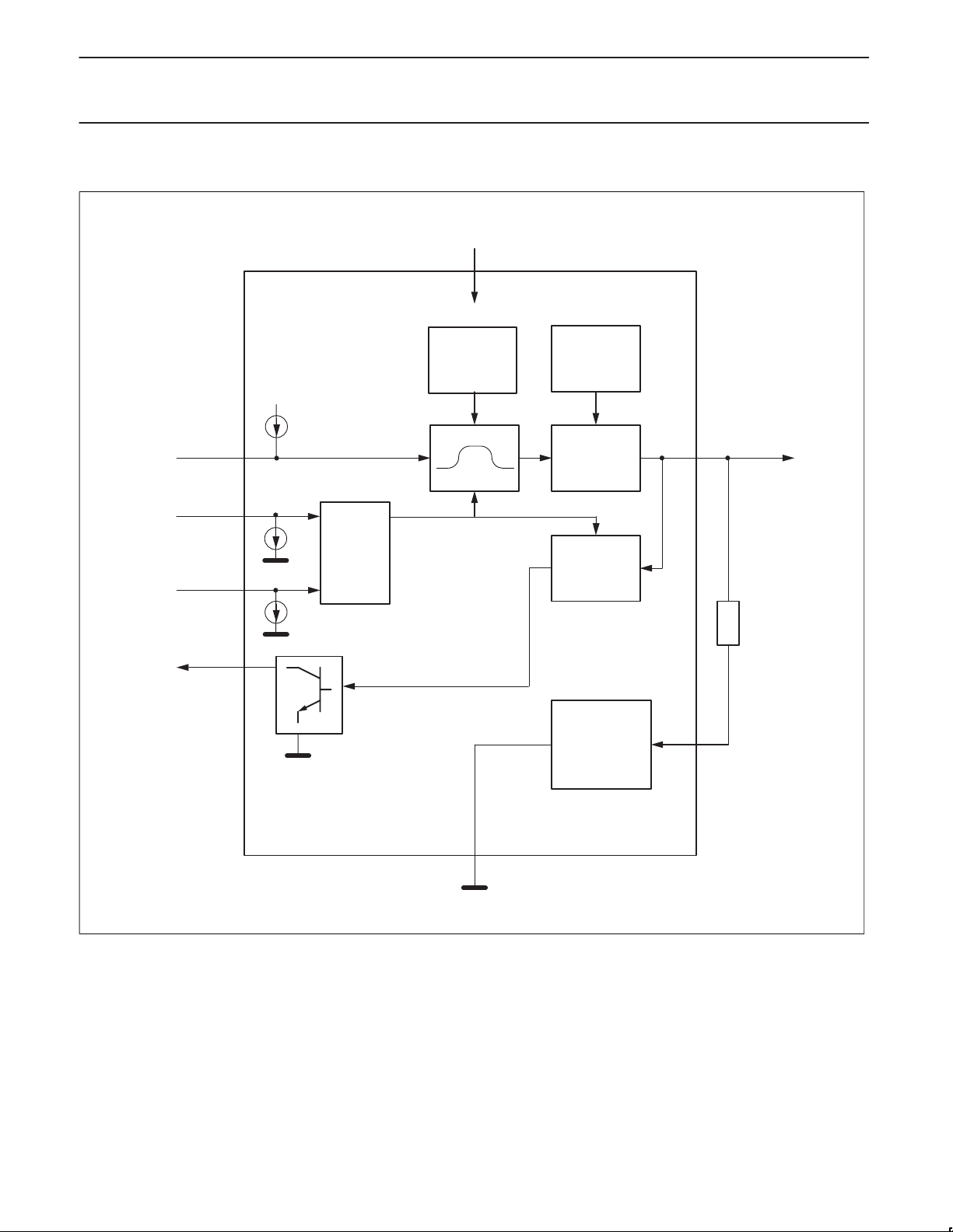
BLOCK DIAGRAM
BATTERY (+12V)
BAT
1
TxD
NSTB
(Mode 0)
(Mode 1)
RxD
EN
VOLTAGE
REFERENCE
3
MODE
6
4
CONTROL
TEMP.
PROTECTION
OUTPUT
BUFFER
BUS
RECEIVER
LOSS OF
GROUND
PROTECTION
CANH
(BUS)
7
R
T
5
RTH
(LOAD)
2001 May 18
AU5790
8
GND
SL01199
Figure 1. Block Diagram
3
Page 4
Philips Semiconductors Product data
AU5790Single wire CAN transceiver
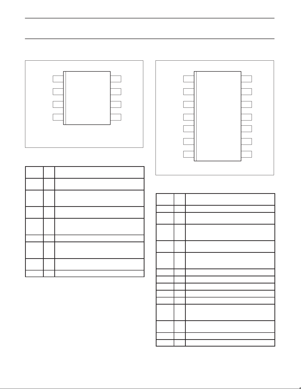
SO8 PIN CONFIGURA TION
TxD
NSTB (Mode 0)
1
2
8
7
GND
CANH (BUS)
AU5790
EN (Mode 1)
RxD
3
4
SO8
6
5
RTH (Load)
BAT
SL01198
SO8 PIN DESCRIPTION
SYM-
BOL
TxD 1 Transmit data input: high = transmitter passive;
NSTB
(Mode 0)
EN
(Mode 1)
RxD 4 Receive data output: low = active bus condition
BAT 5 Battery supply input (12 V nom.)
RTH
(LOAD)
CANH
(BUS)
GND 8 Ground
PIN DESCRIPTION
low = transmitter active
2 Stand-by control: high = normal and
high-speed mode; low = sleep and wake-up
mode
3 Enable control: high = normal and wake-up
mode; low = sleep and high-speed mode
detected; float/high = passive bus condition
detected
6 Switched ground pin: pulls the load to ground,
except in case the module ground is
disconnected
7 Bus line transmit input/output
SO14 PIN CONFIGURATION
GND
TxD
NSTB (Mode 0)
EN (Mode 1)
RxD
N.C.
GND
1
2
3
4
5
6
7
AU5790
SO14
14
13
12
11
10
9
8
GND
N.C.
CANH (BUS)
RTH (Load)
BAT
N.C.
GND
SL01251
SO14 PIN DESCRIPTION
SYM-
BOL
GND 1 Ground
TxD 2 Transmit data input: high = transmitter passive;
NSTB
(Mode 0)
EN
(Mode 1)
RxD 5 Receive data output: low = active bus condition
N.C. 6 No connection
GND 7 Ground
GND 8 Ground
N.C. 9 No connection
BAT 10 Battery supply input (12 V nom.)
RTH
(LOAD)
CANH
(BUS)
N.C. 13 No connection
GND 14 Ground
PIN DESCRIPTION
low = transmitter active
3 Stand-by control: high = normal and
high-speed mode; low = sleep and wake-up
mode
4 Enable control: high = normal and wake-up
mode; low = sleep and high-speed mode
detected; float/high = passive bus condition
detected
11 Switched ground pin: pulls the load to ground,
except in case the module ground is
disconnected
12 Bus line transmit input/output
2001 May 18
4
Page 5

Philips Semiconductors Product data
AU5790Single wire CAN transceiver
FUNCTIONAL DESCRIPTION
The AU5790 is an integrated line transceiver IC that interfaces a
CAN protocol controller to the vehicle’s multiplexed bus line. It is
primarily intended for automotive “Class B” multiplexing applications
in passenger cars using a single wire bus line with ground return.
The achievable bit rate is primarily a function of the network time
constant and the bit timing parameters. For example, the maximum
bus speed is 33 kpbs with bus loading as specified in J2411 for a full
32 node bus, while 41.6 kbps at is possible with modified bus
loading. The AU5790 also supports low-power sleep mode to help
meet ignition-off current draw requirements.
The protocol controller feeds the transmit data stream to the
transceiver’s TxD input. The AU5790 transceiver converts the TxD
data input to a bus signal with controlled slew rate and waveshaping
to minimize emissions. The bus output signal is transmitted via the
CANH in/output, connected to the physical bus line. If TxD is low,
then a typical voltage of 4 V is output at the CANH pin. If TxD is high
then the CANH output is pulled passive low via the local bus load
resistance R
module ground, the resistor R
AU5790. By providing this switched ground pin, no current can flow
from the floating module ground to the bus. The bus receiver detects
the data stream on the bus line. The data signal is output at the RxD
pin being connected to a CAN controller. The AU5790 provides
appropriate filtering to ensure low susceptibility against
electromagnetic interference. Further enhancement is possible with
applying an external capacitor between CANH and ground potential.
The device features low bus output leakage current at power supply
failure situations.
If the NSTB and EN control inputs are pulled low or floating, the
AU5790 enters a low-power or “sleep” mode. This mode is
dedicated to minimizing ignition-off current drain, to enhance system
efficiency. In sleep mode, the bus transmit function is disabled, e.g.
the CANH output is inactive even when TxD is pulled low. An
internal network active detector monitors the bus for any occurrence
. To provide protection against a disconnection of the
T
is connected to the RTH pin of the
T
of signal edges on the bus line. If such edges are detected, this will
be signalled to the CAN controller via the RxD output. Normal
transmission mode will be entered again upon a high level being
applied to the NSTB and EN control inputs. These signals are
typically being provided by a controller device.
Sleeping bus nodes will generally ignore normal communication on
the bus. They should be activated using the dedicated wake-up
mode. When NSTB is low and EN is high the AU5790 enters
wake-up mode i.e. it sends data with an increased signal level. This
will result in an activation of other bus nodes being attached to the
network.
The AU5790 also provides a high-speed transmission mode
supporting bit rates up to 100 kbps. If the NSTB input is pulled high
and the EN input is low, then the internal waveshaping function is
disabled, i.e. the bus driver is turned on and off as fast as possible
to support high-speed transmission of data. Consequently, the EMC
performance is degraded in this mode compared to the normal
transmission mode. In high-speed transmission mode the AU5790
supports the same bus signal level as specified for the CANH output
in normal mode.
The AU5790 features special robustness at its BAT and CANH pins.
Hence the device is well suited for applications in the automotive
environment. The BA T input is protected against 40 V load dump
and jump start condition. The CANH output is protected against
wiring fault conditions, e.g., short circuit to ground or battery voltage,
as well as typical automotive transients. In addition, an
over-temperature shutdown function with hysteresis is incorporated
protecting the device under system fault conditions. In case of the
chip temperature reaching the trip point, the AU5790 will latch-off
the transmit function. The transmit function is available again after a
small decrease of the chip temperature. The AU5790 contains a
power-on reset circuit. For V
< 2.5 V, the CANH output drive will
bat
be turned off, the output will be passive, and RxD will be high. For
2.5 V < V
< 5.3 V, the CANH output drive may operate normally or
bat
be turned off.
Table 1. Control Input Summary
NSTB EN TxD Description CANH RxD
0 0 Don’t Care Sleep mode 0 V float (high)
0 1 Tx-data Wake-up transmission mode 0 V, 12 V bus state
1 0 Tx-data High-speed transmission mode 0 V, 4 V bus state
1 1 Tx-data Normal transmission mode 0 V, 4 V bus state
NOTE:
1. RxD outputs the bus state. If the bus level is below the receiver threshold (i.e., all transmitters passive), then RxD will be floating (i.e., high,
considering external pull-up resistance). Otherwise, if the bus level is above the receiver threshold (i.e., at least one transmitter is active),
then RxD will be low.
2001 May 18
5
1
1
1
Page 6

Philips Semiconductors Product data
AU5790Single wire CAN transceiver
ABSOLUTE MAXIMUM RATINGS
According to the IEC 134 Absolute Maximum System: operation is not guaranteed under these conditions; all voltages are referenced to
pin 8 (GND); positive currents flow into the IC, unless otherwise specified.
SYMBOL
V
BAT
V
BATld
V
BATtr2
V
BATtr3
V
CANH_1
V
CANH_0
V
CANHtr1
V
CANHtr2
V
CANHtr3
V
RTH1
V
RTH0
V
I
ESD
BAHB
ESD
CHHB
ESD
RTHB
ESD
LGHB
R
Tmin
T
amb
T
stg
T
vj
Supply voltage Steady state –0.3 +27 V
Short-term supply voltage Load dump; ISO7637/1 test pulse 5
Transient supply voltage ISO 7637/1 test pulse 2 (SAE J1113,
Transient supply voltage ISO 7637/1 pulses 3a and 3b
CANH voltage V
CANH voltage V
Transient bus voltage ISO 7637/1 test pulse 1, Notes 1 and 2 –100 V
Transient bus voltage ISO 7637/1 test pulse 2, Notes 1 and 2 +100 V
Transient bus voltage ISO 7637/1 test pulses 3a, 3b,
Pin RTH voltage V
Pin RTH voltage V
DC voltage on pins TxD, EN, RxD, NSTB –0.3 +7 V
ESD capability of pin BAT Direct contact discharge,
ESD capability of pin CANH Direct contact discharge,
ESD capability of pin RTH Direct contact discharge,
ESD capability of pins TxD, NSTB, EN, RxD, and
RTH
Bus load resistance RT being connected to pin
RTH
Operating ambient temperature –40 +125
Storage temperature –40 +150 °C
Junction temperature –40 +150 °C
NOTES:
1. Test pulses are coupled to CANH through a series capacitance of 1 nF.
2. Rise time for test pulse 1: t
PARAMETER CONDITIONS MIN. MAX. UNIT
+40 V
(SAE J1113, test pulse 5), T < 1s
+100 V
test pulse 2), with series diode and
bypass cap of 100 nF between BAT and
GND pins, Note 2.
–150 +100 V
(SAE J1113 test pulse 3a and 3b),
Note 2.
> 2 V –10 +18 V
BAT
< 2 V –16 +18 V
BAT
–150 +100 V
Notes 1 and 2
> 2 V, voltage applied to pin RTH
BAT
via a 2 kΩ series resistor
< 2 V, voltage applied to pin RTH
BAT
via a 2 kΩ series resistor
–10 +18 V
–16 +18 V
–8 +8 kV
R=1.5 kΩ, C=100 pF
–8 +8 kV
R=1.5 kΩ, C=100 pF
–8 +8 kV
R=1.5 kΩ + 3 kΩ, C=100 pF
Direct contact discharge,
–2 +2 kV
R=1.5 kΩ , C=100 pF
2 kΩ
< 1 µs; pulse 2: tr < 100 ns; pulses 3a/3b: tr < 5 ns.
r
°C
2001 May 18
6
Page 7

Philips Semiconductors Product data
AU5790Single wire CAN transceiver
DC CHARACTERISTICS
–40 °C < T
–1 V < V
< 13.7 nF; 1µs < RL ∗ CL < 4µs; RxD pull-up resistor 2.2 kΩ < Rd < 3.0 kΩ; RxD: loaded with CLR < 30pF to GND;
C
L
all voltages are referenced to pin 8 (GND); positive currents flow into the IC;
typical values reflect the approximate average value at V
SYMBOL
Pin BAT
V
BAT
V
BATL
V
BATLO
I
BATPN
I
BATPW
I
BATPH
I
BATN
I
BATW
I
BATH
I
BATS
Pin CANH
V
CANHN
V
CANHW
V
CANHWL
V
CANHH
I
CANHRR
I
CANHRD
I
CANHDD
–I
CANH_N
–I
CANHW
< +125 °C; 5.5 V < V
amb
< +16 V; bus load resistor at pin RTH: 2 kΩ < RT < 9.2 kΩ; total bus load resistance 270 Ω < RL < 9.2 kΩ;
CANH
< 16 V; –0.3 V < V
BAT
< 5.5 V; –0.3 V < V
TxD
= 13 V and T
BAT
< 5.5 V; –0.3 V < VEN < 5.5 V; –0.3 V < V
NSTB
= 25 °C, unless otherwise specified.
amb
PARAMETER CONDITIONS MIN. TYP. MAX. UNIT
Operating supply voltage Note 1 5.3 13 27 V
Low battery state Part functional or in undervoltage
2.5 5.3 V
lockout state
Supply undervoltage lockout state TxD = 1 or 0; check CANH and
RxD are floating
Passive state supply current in
NSTB = 5 V, EN = 5 V, TxD = 5 V 2 mA
normal mode
Passive state supply current in
wake-up mode
Passive state supply current in
high speed mode
Active state supply current in
normal mode
Active state supply current in
wake-up mode
Active state supply current in
high speed mode
NSTB = 0 V, EN = 5 V, TxD = 5 V,
Note 2
NSTB = 5 V, EN = 0 V, TxD = 5 V,
Note 2
NSTB = 5 V, EN = 5 V, TxD = 0 V,
R
= 270 Ω, T
L
T
= 25 °C, –40 °C 40 mA
amb
= 125 °C
amb
NSTB = 0 V, EN = 5 V, TxD = 0 V,
R
= 270 Ω, Note 2,
L
= 125 °C
T
amb
T
= 25 °C, –40 °C, Note 2 90 mA
amb
NSTB = 5 V, EN = 0 V, TxD = 0 V,
RL = 100 Ω, Note 2,
T
= 125 °C
amb
T
= 25 °C, –40 °C, Note 2 85 mA
amb
Sleep mode supply current NSTB = 0 V, EN = 0 V, TxD = 5 V,
CANH
BAT
BAT
BAT
BAT
< 11.3 V
< 16 V
BAT
BAT
< +1 V,
< 27 V
< 16 V
< 27 V
< 16 V
3.65 4.1 4.55 V
9.80 min
V
–
BAT
1.45
3.65 4.55 V
–10 10 µA
–20 100 µA
–20 100 µA
30 150 mA
60 190 mA
Bus output voltage in normal
mode
Bus output voltage in wake-up
mode
Bus output voltage in wake-up
mode, low battery
Bus output voltage in high-speed
transmission mode
Recessive state output current,
bus recessive
Recessive state output current,
bus dominant
Dominant state output current,
bus dominant
Bus short circuit current,
normal mode
Bus short circuit current,
wake-up mode
RxD = 5 V, –1 V < V
5.5 V < V
–40 °C < Tj < 125 °C
BAT
< 14 V
NSTB = 5 V, EN = 5 V,
> 270Ω; 5.5 V < V
R
L
NSTB = 0 V, EN = 5 V,
R
> 270Ω; 11.3 V < V
L
NSTB = 0 V, EN = 5 V,
> 270Ω; 5.5 V < V
R
L
NSTB = 5 V, EN = 0 V,
> 100Ω; 8 V < V
R
L
Recessive state or sleep mode,
V
= –1 V; 0 V < V
CANH
Recessive state or sleep mode,
= 10 V; 0 V < V
V
CANH
TxD = 0 V, normal mode,
high-speed mode and sleep mode;
= 10 V;
V
CANH
0 V < V
V
CANH
TxD = 0 V; NSTB = 5 V; EN = 5 V
V
CANH
TxD = 0 V; NSTB = 0 V; EN = 5 V
< 16 V
BAT
= –1 V,
= –1 V,
< 5.5 V;
RxD
2.5 V
3 mA
4 mA
35 mA
70 mA
70 mA
70 100 µA
(V
, 13)
BAT
V
BAT
V
V
2001 May 18
7
Page 8

Philips Semiconductors Product data
AU5790Single wire CAN transceiver
SYMBOL UNITMAX.TYP.MIN.CONDITIONSPARAMETER
Pin CANH (continued)
–I
CANHH
I
CANLG
Bus short circuit current in
high-speed mode
Bus leakage current at loss of
ground
(I_CAN_LG = I_CANH + I_RTH)
T
sd
T
hys
V
T
V
TL
V
TS
V
TSL
Thermal shutdown Note 2 155 190 °C
Thermal shutdown hysteresis Note 2 5 15 °C
Bus input threshold 5.8 V < V
Bus input threshold, low battery 5.5 V < V
Bus input threshold in sleep mode NSTB = 0 V, EN = 0 V,
Bus input threshold in sleep mode,
low battery
Pin RTH
V
V
RTH1
RTH2
Voltage on switched ground pin I
Voltage on switched ground pin I
Pins NSTB, EN
V
ih
V
il
I
i
High level input voltage 5.5 V < V
Low level input voltage 5.5 V < V
Input current Vi = 1 V and Vi = 5 V 15 50 µA
Pin TxD
V
itxd
–I
iltxd
–I
ihtxd
TxD input threshold 5.5 V < V
TxD low level input current in
normal mode
TxD high level input current in
sleep mode
Pin RxD
V
olrxd
I
olrxd
I
ohrxd
RxD low level output voltage I
RxD low level output current V
RxD high level leakage V
NOTES:
1. Operation at battery voltages down to 5.3 volts is guaranteed by design. Operation higher than 18 volts (18 V < V
minutes is permitted if the thermal design of the board prevents reaching the thermal protection temperature limit, T
will self protect. Typically these requirements will be encountered during jump start operation at T
“Thermal Characteristics” section of this data sheet, or application note AN2005 for guidance.
2. This parameter is characterized but not subject to production test.
V
= –1 V,
CANH
TxD = 0 V; NSTB = 5 V; EN = 0 V;
8 V < V
0 V < V
see Figure 3 in the test circuits
BAT
BAT
< 16 V
< 16 V;
50 190 mA
–50 50 µA
section
< 27 V,
all modes except sleep mode
all modes except sleep mode
BAT
BAT
< 5.8 V,
1.8 2.2 V
1.5 2.2 V
6.15 8.1 V
> 11.3 V
V
BAT
NSTB = 0 V, EN = 0 V,
5.5 V < V
= 1 mA 0.1 V
RTH
= 6 mA 1 V
RTH
NSTB = 5 V, EN = 5 V, V
NSTB = 0 V, EN = 0 V, V
= 2.2 mA;
RxD
V
CANH
RxD
RxD
all modes
< 11.3 V
BAT
< 27 V 3 V
BAT
< 27 V 1 V
BAT
< 27 V 1 3 V
BAT
= 0 V 50 180 µA
TxD
= 5 V –5 10 µA
TxD
= 10 V, all modes
= 5 V; V
= 5 V; V
= 10 V 3 35 mA
CANH
= 0 V,
CANH
V
– 4.3 V
BAT
– 3.25 V
BAT
0.45 V
–10 +10 µA
< 27 V) for up to two
BAT
, otherwise the device
85 °C and V
amb
sd
< 27 V. Refer to the
BAT
2001 May 18
8
Page 9

Philips Semiconductors Product data
AU5790Single wire CAN transceiver
Dynamic (AC) CHARACTERISTICS for 33 kbps operation
–40 °C < T
–1 V < V
< 13.7 nF; 1µs < RL ∗ CL < 4µs; RxD pull-up resistor 2.2 kΩ < Rd < 3.0 kΩ; RxD: loaded with CLR < 30pF to GND;
C
L
all voltages are referenced to pin 8 (GND); positive currents flow into the IC;
typical values reflect the approximate average value at V
SYMBOL
Pin CANH
V
dBAMN
V
dBAMW
Pins NSTB, EN
t
NH
t
HN
t
WN
t
NS
t
SN
Pin TxD
t
TrN
t
TfN
t
TrW
t
TrW-S
t
TfW-3.6
t
TfW-4.0
< +125 °C; 5.5 V < V
amb
< +16 V; bus load resistor at pin RTH: 2 kΩ < RT < 9.2 kΩ; total bus load resistance 270 Ω < RL < 9.2 kΩ;
CANH
< 16 V; –0.3 V < V
BAT
< 5.5 V; –0.3 V < V
TxD
= 13 V and T
BAT
< 5.5 V; –0.3 V < VEN < 5.5 V; –0.3 V < V
NSTB
= 25 °C, unless otherwise specified.
amb
PARAMETER CONDITIONS MIN. TYP. MAX. UNIT
CANH harmonic content in
normal mode
CANH harmonic content in
wake-up mode
NSTB = 5 V, EN = 5 V;
= 270 Ω, CL = 15 nF;
R
L
f
= 20 kHz, 50% duty cycle;
TxD
8 V < V
0.53 MHz < f < 1.7 MHz, Note 2
BAT
< 16 V;
NSTB = 5 V, EN = 0 V;
R
= 270 Ω, CL = 15 nF;
L
= 20 kHz, 50% duty cycle;
f
TxD
8 V < V
0.53 MHz < f < 1.7 MHz, Note 2
BAT
< 16 V;
Normal mode to high-speed mode
delay
High-speed mode to normal mode
delay
Wake-up mode to normal mode
delay
8 V < V
< 16 V 30 µs
BAT
Normal mode to sleep mode delay 500 µs
Sleep mode to normal mode delay 50 µs
Transmit delay in normal mode,
bus rising edge
Transmit delay in normal mode,
bus falling edge
Transmit delay in wake-up mode,
bus rising edge to normal levels
Transmit delay in wake-up mode,
bus rising edge to wake-up level
Transmit delay in wake-up mode,
bus falling edge with 3.6 µs time
constant
Transmit delay in wake-up mode,
bus falling edge with 4.0 µs time
constant
NSTB = 5 V, EN = 5 V;
= 270 Ω, CL = 15 nF;
R
L
5.5 V < V
measured from the falling edge on
TxD to V
BAT
CANH
< 27 V;
= 3.0 V
NSTB = 5 V, EN = 5 V;
R
= 270 Ω, CL = 15 nF;
L
5.5 V < V
measured from the rising edge on
TxD to V
BAT
CANH
< 27 V;
= 1.0 V
NSTB = 0 V, EN = 5 V;
= 270 Ω, CL = 15 nF;
R
L
5.5 V < V
measured from the falling edge on
TxD to V
BAT
CANH
< 27 V;
= 3.0 V
NSTB = 0 V, EN = 5 V;
R
= 270 Ω, CL = 15 nF;
L
11.3 V < V
measured from the falling edge on
TxD to V
BAT
CANH
< 27 V;
= 8.9 V
NSTB = 0 V, EN = 5 V;
= 270 Ω, CL = 13.3 nF;
R
L
5.5 V < V
measured from the rising edge on
TxD to V
< 27 V;
BAT
= 1 V, Note 2
CANH
NSTB = 0 V, EN = 5 V;
R
= 270 Ω, CL = 15 nF;
L
5.5 V < V
measured from the rising edge on
TxD to V
BAT
CANH
< 27 V;
= 1 V
3 6.3 µs
3 9 µs
3 6.3 µs
3 18 µs
3 12.7 µs
3 13.7 µs
< 5.5 V;
RxD
70 dBµV
80 dBµV
30 µs
30 µs
2001 May 18
9
Page 10

Philips Semiconductors Product data
AU5790Single wire CAN transceiver
SYMBOL UNITMAX.TYP.MIN.CONDITIONSPARAMETER
Pin TxD (continued)
t
TrHS
t
TfHS
Pin RxD
t
DN
t
DW
t
DHS
t
DS
NOTES:
1. Operation at battery voltages down to 5.3 volts is guaranteed by design. Operation higher than 18 volts (18 V < V
minutes is permitted if the thermal design of the board prevents reaching the thermal protection temperature limit, T
will self protect. Typically these requirements will be encountered during jump start operation at T
“Thermal Characteristics” section of this data sheet, or application note AN2005 for guidance.
2. This parameter is characterized but not subject to production test.
Transmit delay in high-speed
mode, bus rising edge
Transmit delay in high-speed
mode, bus falling edge
Receive delay in normal mode,
bus rising and falling edge
Receive delay in wake-up mode,
bus rising and falling edge
Receive delay in high-speed
mode, bus rising and falling edge
Receive delay in sleep mode,
bus rising edge
NSTB = 5 V, EN = 0 V;
= 100 Ω, CL = 15 nF;
R
L
8 V < V
measured from the falling edge on
TxD to V
BAT
CANH
< 16 V;
= 3.0 V
NSTB = 5 V, EN = 0 V;
= 100 Ω, CL = 15 nF;
R
L
8 V < V
measured from the rising edge on
TxD to V
BAT
CANH
< 16 V;
= 1.0 V
NSTB = 5 V, EN = 5 V;
5.5 V < V
CANH to RxD time measured from
V
CANH
< 27 V;
BAT
= 2.0 V to V
RxD
= 2.5 V
NSTB = 0 V, EN = 5 V;
5.5 V < V
CANH to RxD time measured from
V
CANH
< 27 V;
BAT
= 2.0 V to V
RxD
= 2.5 V
NSTB = 5 V, EN = 0 V;
8 V < V
CANH to RxD time measured from
V
CANH
< 16 V;
BAT
= 2.0 V to V
RxD
= 2.5 V
NSTB = 0 V, EN = 0 V;
CANH to RxD time, measured from
= min {(V
V
CANH
7.13 V} to V
RxD
– 3.78 V),
BAT
= 2.5 V
0.1 1.5 µs
0.2 3 µs
0.3 1 µs
0.3 1 µs
0.3 1 µs
10 70 µs
< 27 V) for up to two
BAT
, otherwise the device
85 °C and V
amb
sd
< 27 V. Refer to the
BAT
2001 May 18
10
Page 11
Philips Semiconductors Product data
AU5790Single wire CAN transceiver
TxD
50%
t
Tr
CANH
3 V
2 V
1 V
t
RxD
50%
D
NOTE:
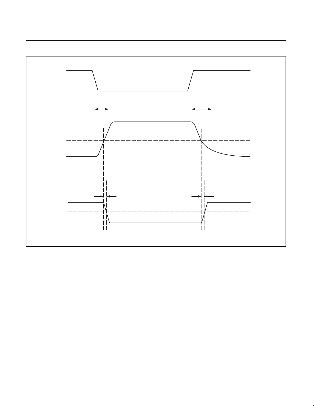
1. When AU5790 is in normal, high-speed, or wake-up mode, the transmit delay in rising edge t
respectively; the transmit delay in falling edge t
, or tDW, respectively.
t
DHS
may be expressed as t
Tf
TfN
, t
TfHS
, or t
, respectively; and the receive delay tD as tDN,
TfW
Figure 2. Timing Diagrams: Pin TxD, CANH, and RxD
t
Tf
t
D
may be expressed as t
Tr
SL01255
TrN
, t
, or t
TrHS
TrW
,
2001 May 18
11
Page 12
Philips Semiconductors Product data
AU5790Single wire CAN transceiver
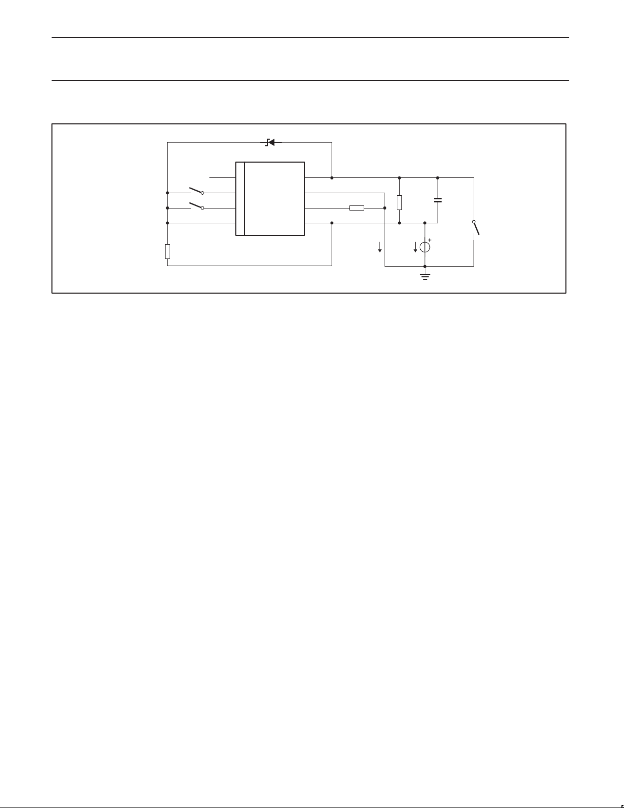
TEST CIRCUITS
5.1V
2.4 kΩ
TxD
S1
NSTB
EN
S2
RxD
AU5790
GND
CANH
RTH
BAT
9.1 kΩ
I_CAN_LG
Figure 3. Loss of ground test circuit
NOTES:
Opening S3 simulates loss of module ground.
Check I_CAN_LG with the following switch positions to simulate loss of ground in all modes:
1. S1 = open = S2
2. S1 = open, S2 = closed
3. S1 = closed, S2 = open
4. S1 = closed = S2
1.5 k
1 µF
S3
V
BAT
SL01234
2001 May 18
12
Page 13
Philips Semiconductors Product data
AU5790Single wire CAN transceiver
APPLICATION INFORMATION
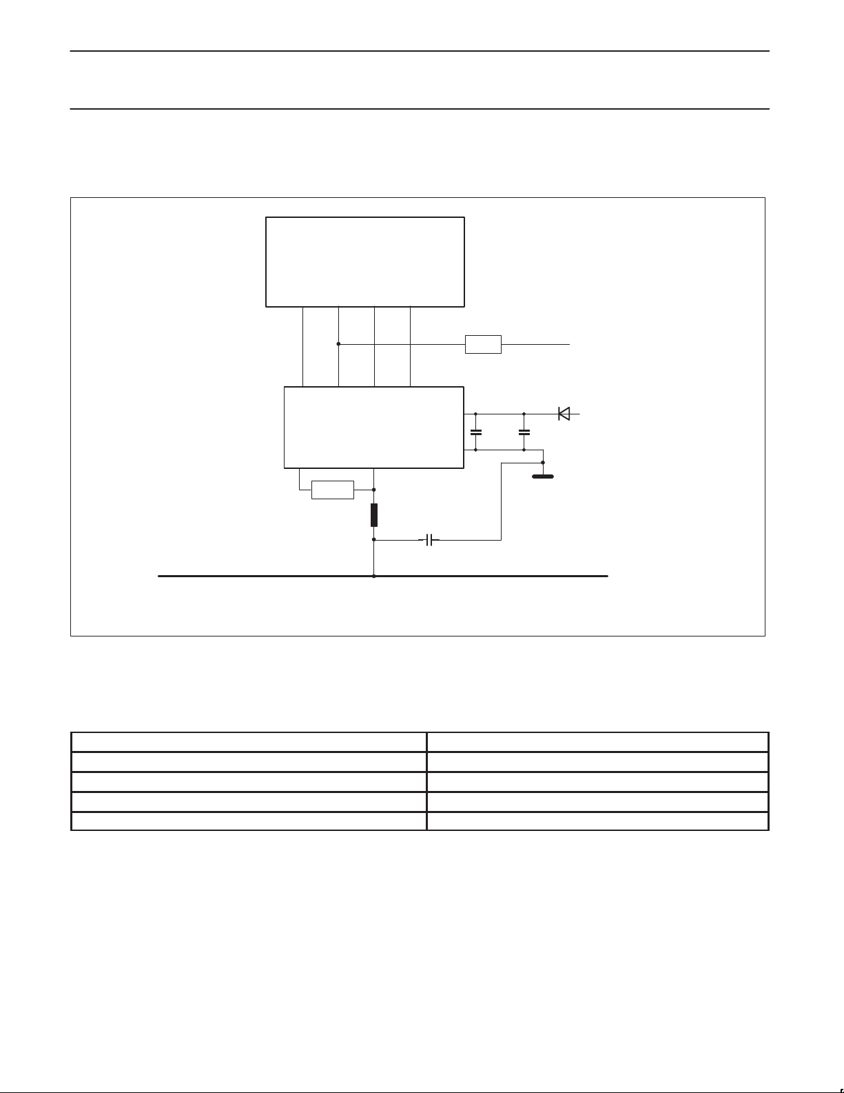
The information in this section is not part of the IC specification, but is presented for information purposes only. Additional information on single
wire CAN networks, application circuits, and thermal management are included in application note AN2005.
CAN CONTROLLER
(e.g. SJA1000)
PORT
AU5790
TRANSCEIVER
1%
R
T
CANH
L
PORT
47 µH
10%
ENNSTB
220 pF
R
D
2.4 to
2.7kΩ
BAT
GND
C
L
100 nF
1N5060
or equiv.
1 to 4.7 µF
+5V
+12V
TX0 RX0
TxD RxD
RTH
9.1kΩ,
CAN BUS LINE
Note 1 TX0 should be configured to push-pull operation, active low; e.g., Output Control Register = 1E hex.
Note 2 Recommended range for the load resistor is 3k < R
< 11k.
T
SL01200
Figure 4. Application circuit example for the AU5790
AU5790 transceivers may require additional PCB surface at ground pin(s) as heat conductor(s) in order to meet thermal requirements. See
thermal characteristics section for details.
Table 2. Maximum CAN Bit Rate
MODE MAXIMUM BIT RATE AT 0.35% CLOCK ACCURACY
Normal transmission 33.3 kbps
High-speed transmission 83.3 kbps
Sample point as % of bit time 85%
Bus Time constant, normal mode 1.0 to 4.0 µs
2001 May 18
13
Page 14
Philips Semiconductors Product data
AU5790Single wire CAN transceiver
T
=T
THERMAL CHARACTERISTICS
The AU5790 provides protection from thermal overload. When the
IC junction temperature reaches the threshold (≈155 °C), the
AU5790 will disable the transmitter drivers, reducing power
dissipation to protect the device. The transmit function will become
available again after the junction temperature drops. The thermal
shutdown hysteresis is about 5 °C.
In order to avoid this transmit function shutdown, care must be taken
to not overheat the IC during application. The relationships between
junction temperature, ambient temperature, dissipated power, and
thermal resistance can be expressed as:
200
+ Pd * θ
j
a
ja
where: Tj is junction temperature (°C);
T
is ambient temperature (°C);
a
P
is dissipated power (W);
d
is thermal resistance (°C/W).
θ
ja
Thermal Resistance
Thermal resistance is the ability of a packaged IC to dissipate heat
to its environment. In semiconductor applications, it is highly
dependant on the IC package, PCBs, and airflow. Thermal
resistance also varies slightly with input power, the difference
between ambient and junction temperatures, and soldering material.
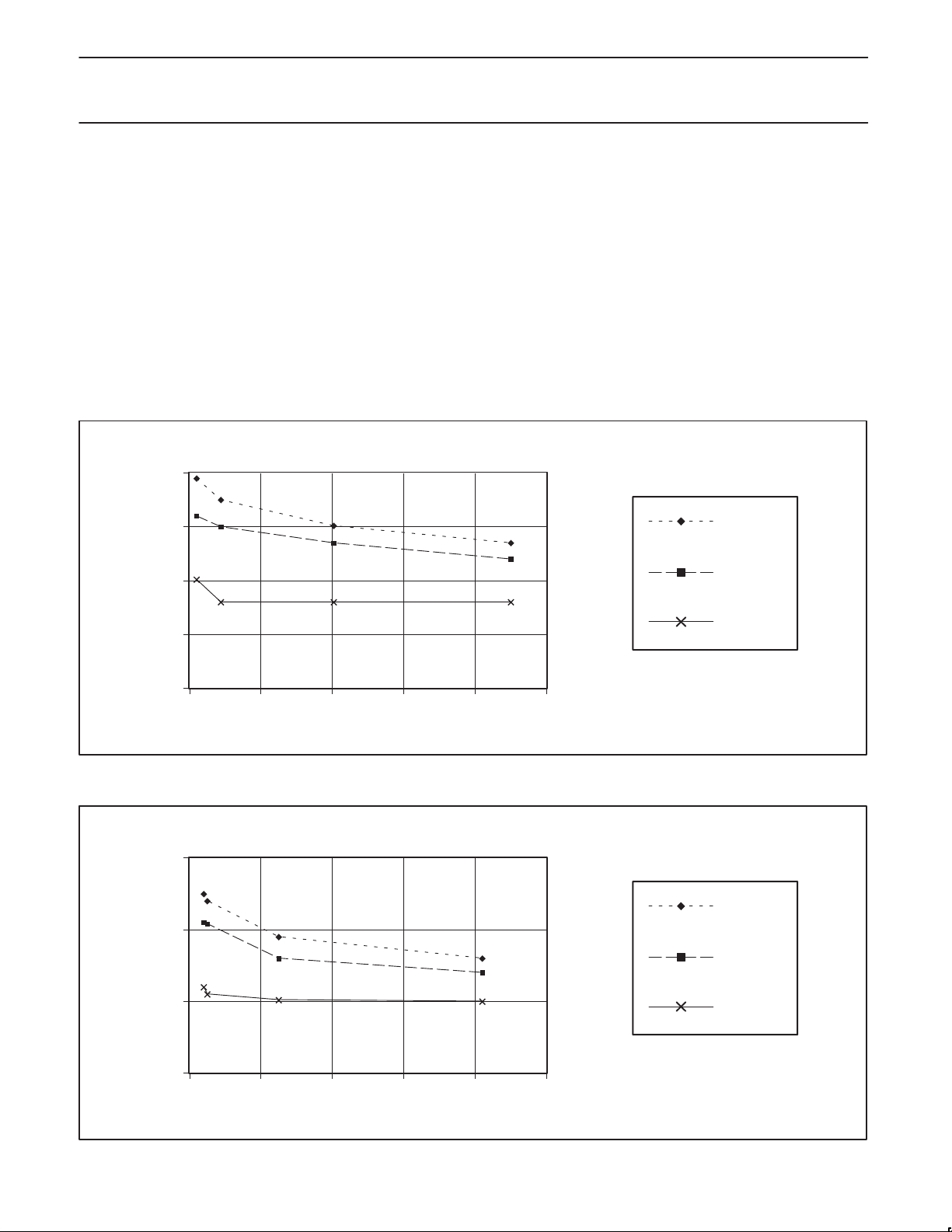
Figures 5 and 6 show the thermal resistance as the function of the
IC package and the PCB configuration, assuming no airflow.
150
100
Thermal resistance (C/W)
50
0
0 50 100 150 200 250
Cu area on fused pins (mm2)
Figure 5. SO-8 Thermal Resistance vs. PCB Configuration, Note 1, 2, 3
150
100
very low
conductance
board
low
conductance
board
high
conductance
board
SL01249
very low
conductance
board
low
conductance
board
2001 May 18
50
Thermal resistance (C/W)
0
0 100 200 300 400 500
Cu area on fused pins (mm2)
Figure 6. SO-14 Thermal Resistance vs. PCB Configuration, Note 1, 2, 3
14
high
conductance
board
SL01250
Page 15

Philips Semiconductors Product data
Additional Foil Area for
Conduct
d
Conduct
d
Conduct
d
Conduct
d
Conduct
d
Conduct
d
AU5790Single wire CAN transceiver
Table 3 shows the maximum power dissipation of an AU5790 without tripping the thermal overload protection, for specified combinations of
package, board configuration, and ambient temperature.
Table 3. Maximum power dissipation
Board Type
SO-8 on High
ance Boar
SO-8 on Low
ance Boar
SO-8 on Very Low
ance Boar
SO-14 on High
ance Boar
SO-14 on Low
ance Boar
SO-14 on Very Low
ance Boar
Θ
JA
Power Dissipation Max.
Additional Foil Area for
Heat Dissipation
Normal traces 103 631 243
225 Sq. mm of copper
foil attached to pin 8.
Normal traces 163 399 153
225 Sq. mm of copper
attached to pin 8.
Normal traces 194 335 129
225 Sq. mm of copper
attached to pin 8.
Normal traces 63 1032 397
105 Sq. mm of copper
attached to each of pins
1, 7, 8, & 14.
Normal traces 103 631 243
105 Sq. mm of copper
attached to each of pins
1, 7, 8, & 14.
Normal traces 126 516 198
105 Sq. mm of copper
attached to each of pins
1, 7, 8, & 14.
Thermal Resistance
K/W mW mW
82 793 305
119 546 210
135 481 185
50 1300 500
70 929 357
82 793 305
Ta= 85 °C Ta= 125 °C
P
tot
NOTES:
1. The High Conductance board is based on modeling done to EIA/JEDEC Standard JESD51-7. The board emulated contains two one ounce
thick copper ground planes, and top surface copper conductor traces of two ounce (0.071 mm thickness of copper).
2. The Low Conductance board is based on modeling done to EIA/JEDEC Standard EIA/JESD51-3. The board does not contain any ground
planes, and the top surface copper conductor traces of two ounce (0.071 mm thickness of copper).
3. The Very Low Conductance board is based on the EIA/JESD51-3, however the thickness of the surface conductors has been reduced to
0.035 mm (also referred to as 1.0 Ounce copper).
4. The above mentioned JEDEC specifications are available from: http://www.jedec.org/
2001 May 18
15
Page 16

Philips Semiconductors Product data
AU5790Single wire CAN transceiver
I
Power Dissipation
Power dissipation of an IC is the major factor determining junction
temperature. AU5790 power dissipation in active and passive states
are different. The average power dissipation is:
P
= P
where: P
INT
*Dy + P
tot
is total dissipation power;
tot
P
is dissipation power in an active state;
INT
P
is dissipation power in a passive state;
PNINT
PNINT
* (1-Dy)
Dy is duty cycle, which is the percentage of time that TxD
is in an active state during any given time duration.
At passive state there is no current going into the load. So
all of the supply current is dissipated inside the IC.
P
= V
BAT
* I
BATPN
where: V
PNINT
is the battery voltage;
BAT
I
is the passive state supply current in normal mode.
BATPN
In an active state, part of the supply current goes to the
load, and only part of the supply current dissipates inside
the IC, causing an incremental increase in junction
temperature.
P
where: P
= P
INT
is active state battery supply power in normal
BATAN
BATAN
– P
LOADN
mode;
= V
BAT
CANHN
* I
BATAN
* I
LOADN
where: I
P
BATAN
P
is load power consumption in normal mode.
LOADN
P
= V
LOADN
is active state supply current in normal mode;
BATAN
V
is bus output voltage in normal mode;
CANHN
I
is current going through load in normal mode.
LOADN
where: I
is an active state current dissipated within the IC in
INT
normal mode.
I
will decrease slightly when the node number
INT
decreases. To simplify this analysis, we will assume I
fixed.
I
= I
INT
BATN
(32 nodes) may be found in the DC Characteristics
I
BATN
table.
A power dissipation example follows. The assumed values
are chosen from specification and typical applications.
Assumptions:
Computations:
R
P
PNINT
I
LOAD
P
LOADN
I
P
BATAN
= 469 mW - 72.8 mW = 396.2 mW
P
P
tot
INT
= 396.2 mW × 50% + 26.8 mW × (1-50%) = 211.5 mW
Additional examples with various node counts are shown in Table 4.
= V
LOAD
CANHN/RLOAD
I
= I
BATN
LOAD
(32 nodes) – I
V
= 13.4 V
BAT
= 9.1 kΩ
R
T
+ I
LOAD
INT
32 nodes
I
= 2 mA
BATPN
I
(32 nodes) = 35 mA
BATN
V
CANHN
= 4.55 V
Duty cycle = 50%
= 9.1 kΩ / 32 = 284.4 Ω
LOAD
= 13.4 V × 2 mA = 26.8 mW
= 4.55 V / 284.4 Ω = 16mA
= 4.55 V × 16 mA = 72.8 mW
= 35 mA - 16 mA = 19 mA
INT
= 13.4 V × 35 mA = 469 mW
(32 nodes)
INT
is
Table 4. Representative Power Dissipation Analyses
R
LOAD
Nodes
(Ω)
V
BAT
2 4550 13.4 2 26.8 4.55 1 20 19 263.5 0.5 145.1
10 910 13.4 2 26.8 4.55 5 24 19 298.9 0.5 162.8
20 455 13.4 2 26.8 4.55 10 29 19 343.1 0.5 184.9
32 284.4 13.4 2 26.8 4.55 16 35 19 396.2 0.5 211.5
2 4550 26.5 2 53 4.55 1 20 19 525.5 0.5 289.2
10 910 26.5 2 53 4.55 5 24 19 613.3 0.5 333.1
20 455 26.5 2 53 4.55 10 29 19 723 0.5 388
32 284.4 26.5 2 53 4.55 16 35 19 854.7 0.5 453.8
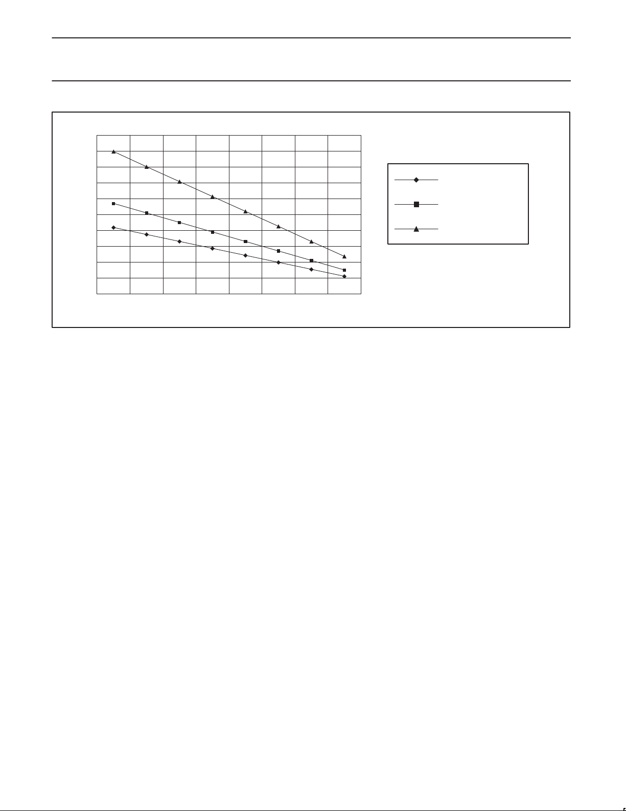
By knowing the maximum power dissipation, and the operation ambient temperature, the required thermal resistance without tripping the
thermal protection can be calculated, as shown in Figure 7. Then from Figure 5 or 6, a suitable PCB can be selected.
2001 May 18
(V)
I
BATPN
(mA)
P
PNINT
(mW)
V
CANHN
(V)
16
I
LOAD
(mA)
I
BATN
(mA)
I
INT
(mA)
P
INT
(mW)
Dcycle
P
tot
(mW)
Page 17
Philips Semiconductors Product data
AU5790Single wire CAN transceiver
500
450
400
350
300
250
200
150
THERMAL RESISTANCE (C/W)
100
50
0
50 60 70 80 90 100 110 120 130
AMBIENT TEMPERATURE (°C)
Ptot = 453.8 mW
(Vbat = 26.5 V, 32 nodes)
Ptot = 333.1 mW
(Vbat = 26.5 V, 10 nodes)
Ptot = 211.5 mW
(Vbat = 13.4 V, 32 nodes)
SL01256
Figure 7. Required Thermal Resistance vs. Ambient Temperature and Power Dissipation
2001 May 18
17
Page 18
Philips Semiconductors Product data
AU5790Single wire CAN transceiver
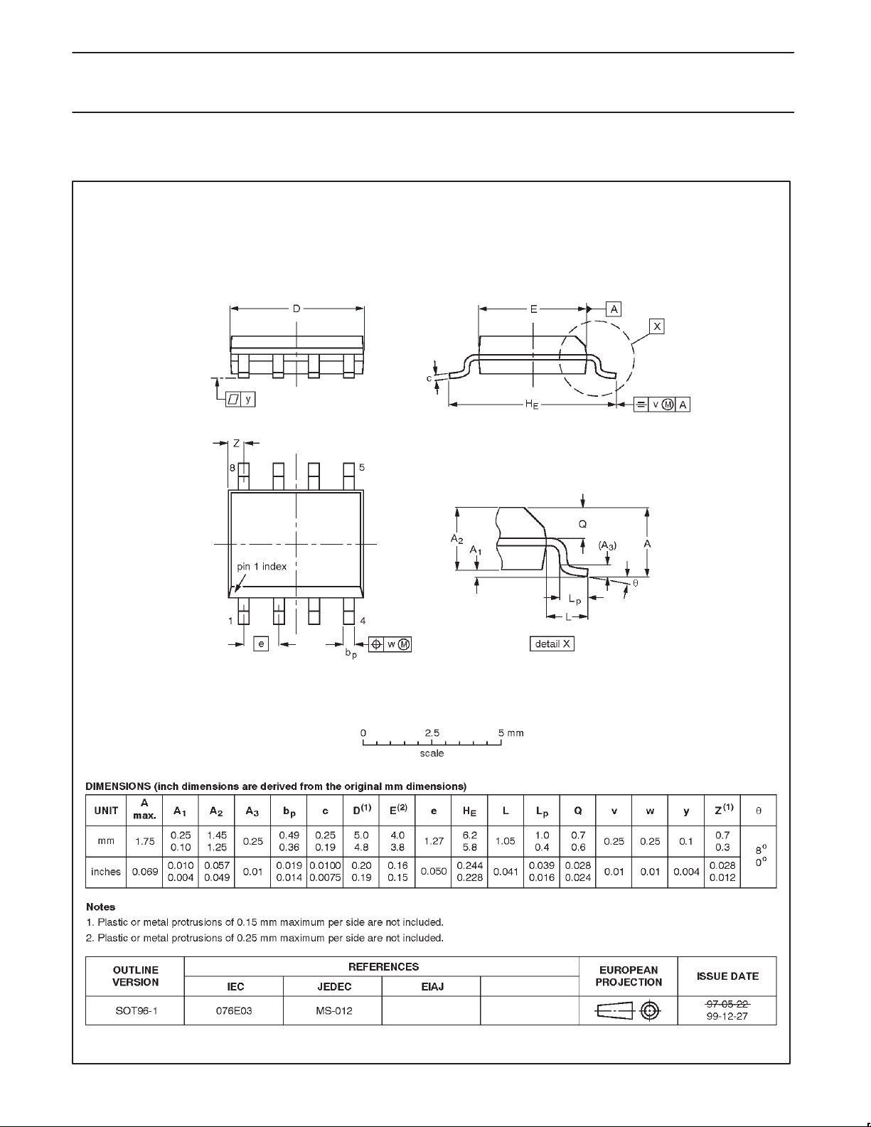
SO8: plastic small outline package; 8 leads; body width 3.9 mm SOT96-1
2001 May 18
18
Page 19
Philips Semiconductors Product data
AU5790Single wire CAN transceiver
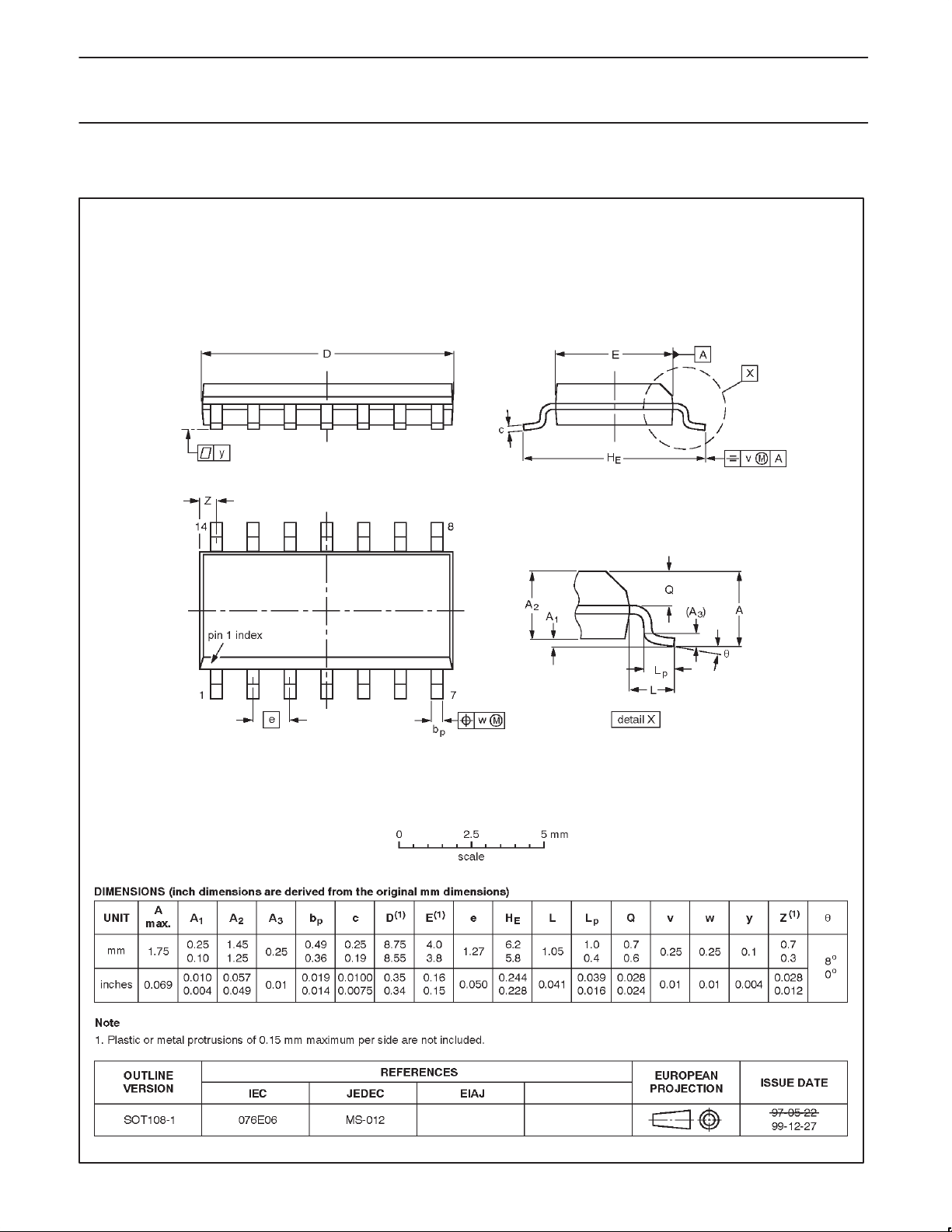
SO14: plastic small outline package; 14 leads; body width 3.9 mm SOT108-1
2001 May 18
19
Page 20

Philips Semiconductors Product data
AU5790Single wire CAN transceiver
Data sheet status
Product
Data sheet status
Objective data
Preliminary data
Product data
[1] Please consult the most recently issued datasheet before initiating or completing a design.
[2] The product status of the device(s) described in this data sheet may have changed since this data sheet was published. The latest information is available on
the Internet at URL http://www.semiconductors.philips.com.
[1]
status
Development
Qualification
Production
[2]
Definitions
Short-form specification — The data in a short-form specification is extracted from a full data sheet with the same type number and title. For
detailed information see the relevant data sheet or data handbook.
Limiting values definition — Limiting values given are in accordance with the Absolute Maximum Rating System (IEC 134). Stress above one
or more of the limiting values may cause permanent damage to the device. These are stress ratings only and operation of the device at these or
at any other conditions above those given in the Characteristics sections of the specification is not implied. Exposure to limiting values for extended
periods may affect device reliability.
Application information — Applications that are described herein for any of these products are for illustrative purposes only. Philips
Semiconductors make no representation or warranty that such applications will be suitable for the specified use without further testing or
modification.
Disclaimers
Life support — These products are not designed for use in life support appliances, devices or systems where malfunction of these products can
reasonably be expected to result in personal injury . Philips Semiconductors customers using or selling these products for use in such applications
do so at their own risk and agree to fully indemnify Philips Semiconductors for any damages resulting from such application.
Right to make changes — Philips Semiconductors reserves the right to make changes, without notice, in the products, including circuits, standard
cells, and/or software, described or contained herein in order to improve design and/or performance. Philips Semiconductors assumes no
responsibility or liability for the use of any of these products, conveys no license or title under any patent, copyright, or mask work right to these
products, and makes no representations or warranties that these products are free from patent, copyright, or mask work right infringement, unless
otherwise specified.
Philips Semiconductors
811 East Arques Avenue
P.O. Box 3409
Sunnyvale, California 94088–3409
Telephone 800-234-7381
Definitions
This data sheet contains data from the objective specification for product development.
Philips Semiconductors reserves the right to change the specification in any manner without notice.
This data sheet contains data from the preliminary specification. Supplementary data will be
published at a later date. Philips Semiconductors reserves the right to change the specification
without notice, in order to improve the design and supply the best possible product.
This data sheet contains data from the product specification. Philips Semiconductors reserves the
right to make changes at any time in order to improve the design, manufacturing and supply.
Changes will be communicated according to the Customer Product/Process Change Notification
(CPCN) procedure SNW-SQ-650A.
Copyright Philips Electronics North America Corporation 2001
All rights reserved. Printed in U.S.A.
Date of release: 05-01
Document order number: 9397 750 08401
2001 May 18
20
 Loading...