

Page 1

INTEGRATED CIRCUITS
AU5780A
SAE/J1850/VPW transceiver
Preliminary specification
Supersedes data of 1998 Feb 11
1999 Jan 28
Page 2
Philips Semiconductors Preliminary specification
AU5780ASAE/J1850/VPW transceiver
FEATURES
•Supports SAE/J1850 VPW standard for in-vehicle class B
multiplexing
•Bus speed 10.4 kbps nominal
DESCRIPTION
The AU5780A is a line transceiver being primarily intended for
in-vehicle multiplex applications. It provides interfacing between a
link controller and the physical bus wire. The device supports the
SAE/J1850 VPWM standard with a nominal bus speed of 10.4 kbps.
•Drive capability 32 bus nodes
•Low RFI due to output waveshaping with adjustable slew rate
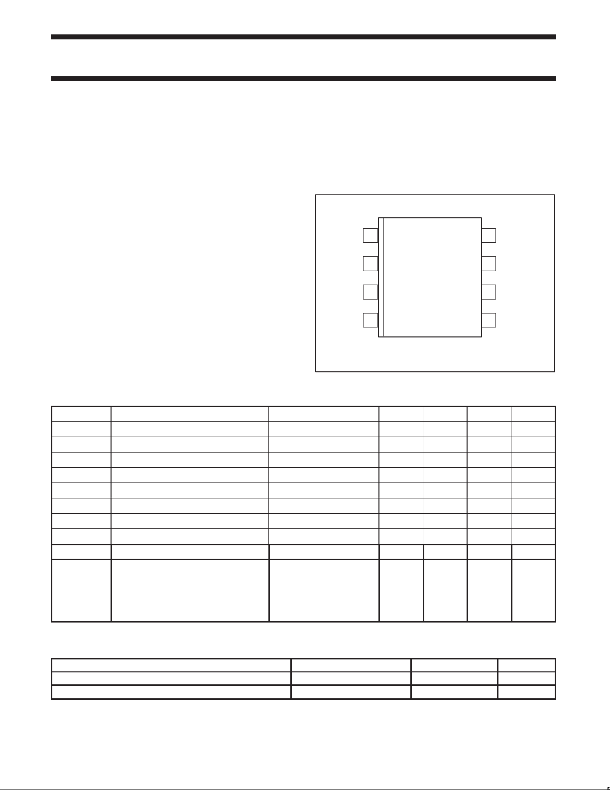
PIN CONFIGURATION
•Direct battery operation with protection against +50V load dump,
jump start and reverse battery
•Bus terminals proof against automotive transients up to
–200V/+200V
BATT
1
8
GND
•Thermal overload protection
•Very low bus idle power consumption
•Diagnostic loop-back mode
R/F
2
TX
AU5780A
3
7
6
BUS_OUT
/LB
•4X mode (41.6 kbps) reception capability
•ESD protected to 9 KV on bus and battery pins
•8-pin SOIC
QUICK REFERENCE DA TA
SYMBOL PARAMETER CONDITIONS MIN. TYP. MAX. UNIT
V
BATT.op
T
A
V
BATT.ld
I
BATT.lp
V
B
V
BOH
–I
BO.LIM
V
BI
t
bo
tr, t
f
Operating supply voltage 6 12 24 V
Operating ambient temperature –40 +125 °C
Battery voltage load dump; 1s +50 V
Bus idle supply current V
Bus voltage 0 < V
Bus output voltage 300Ω < RL < 1.6kΩ 7.3 8.0 V
Bus output source current 0V < VBO < +8.5V 27 50 mA
Bus input threshold 3.65 4.1 V
Delay TX to BUS_OUT, normal battery Measured at 3.875V 13 21 µs
BUS_OUT transition times, rise and fall,
normal battery
=12V 220 µA
BATT
< 24V –20 +20 V
BATT
Measured between
1.5 V and (V
9 < V
t
tested at an additional bus
r
load of R
C
LOAD
BATT
< 16 V,
BATT
LOAD
= 22000 pF
RX
– 2.75 V),
= 400 W and
4
11 18 µs
SO8
5
BUS_IN
SL01207
ORDERING INFORMATION
DESCRIPTION TEMPERATURE RANGE ORDER CODE DWG #
SO8: 8-pin plastic small outline package; Packed in tubes –40 to +125°C AU5780AD SOT96-1
SO8: 8-pin plastic small outline package; Packed on tape & reel –40 to +125°C AU5780AD–T SOT96-1
1999 Jan 28
2
Page 3
Philips Semiconductors Preliminary specification
AU5780ASAE/J1850/VPW transceiver
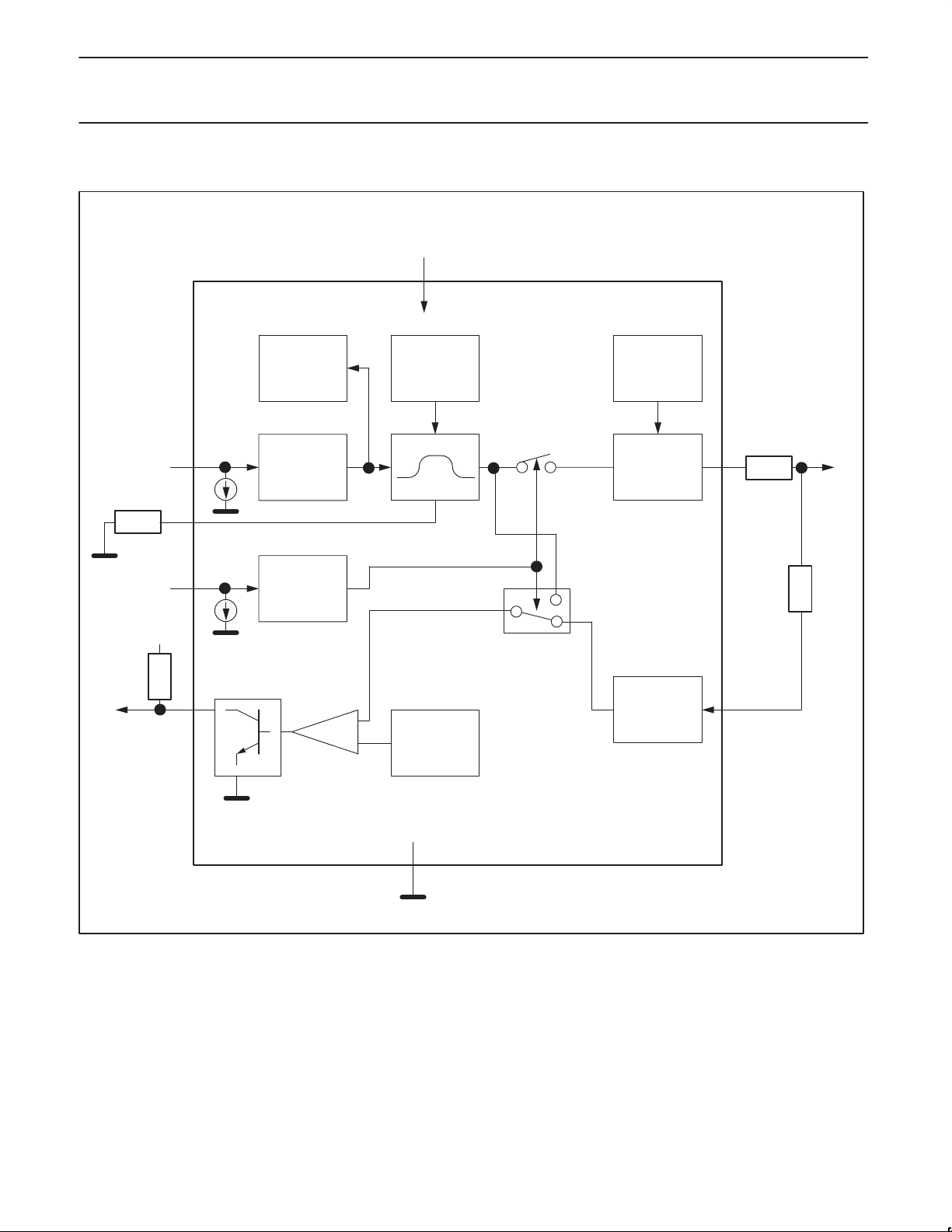
BLOCK DIAGRAM
BATTERY (+12V)
BATT
1
LOW–POWER
TIMER
TX
2
Rs
Vcc
Rd
R/F
/LB
RX
3
6
4
TX–
BUFFER
INPUT
BUFFER
VOLTAGE
REFERENCE
VOLTAGE
REFERENCE
TEMP.
PROTECTION
OUTPUT
BUFFER
INPUT
FILTER
7
5
BUS_OUT
Rb
Rf
BUS_IN
1999 Jan 28
AU5780
8
GND
SL01208
3
Page 4

Philips Semiconductors Preliminary specification
AU5780ASAE/J1850/VPW transceiver
PIN DESCRIPTION
SYMBOL PIN DESCRIPTION
BATT 1 Battery supply input (12V nom.)
TX 2 Transmit data input; low: transmitter passive; high: transmitter active
R/F 3 Rise/fall slew rate set input
RX 4 Receive data output; low: active bus condition detected; float/high: passive bus condition detected
BUS_IN 5 Bus line receive input
/LB 6 Loop-back test mode control input; low: loop-back mode; high: normal communication mode
BUS_OUT 7 Bus line transmit output
GND 8 Ground
FUNCTIONAL DESCRIPTION
The AU5780A is an integrated line transceiver IC that interfaces an
SAE/J1850 protocol controller IC to the vehicle’s multiplexed bus
line. It is primarily intended for automotive “Class B” multiplexing
applications in passenger cars using VPW (Variable Pulse Width)
modulated signals with a nominal bit rate of 10.4 kbps. The
AU5780A also receives messages in the so-called 4X mode where
data is transmitted with a typical bit rate of 41.6 kbps. The device
provides transmit and receive capability as well as protection to a
J1850 electronic module.
A J1850 link controller feeds the transmit data stream to the
transceiver’s TX input. The AU5780A transceiver waveshapes the
TX data input signal with controlled rise & fall slew rates and
rounded shape. The bus output signal is transmitted with both
voltage and current control. The BUS_IN input is connected to the
physical bus line via an external resistor. The external resistor and
an internal capacitance provides filtering against RF bus noise. The
incoming signal is output at the RX pin being connected to the
J1850 link controller.
If the TX input is idle for a certain time, then the AU5780A enters a
low-power mode. This mode is dedicated to help meet ignition-off
current draw requirements. The BUS_IN input comparator is kept
alive in the low-power mode. Normal power mode will be entered
again upon detection of activity, i.e., rising edge at the TX input. The
device is able to receive and transmit a valid J1850 message when
initially in low-power mode.
The AU5780A features special robustness at its BATT and
BUS_OUT pins hence the device is well suited for applications in
the automotive environment. Specifically, the BATT input is
protected against 50V load dump, jump start and reverse battery
condition. The BUS_OUT output is protected against wiring fault
conditions, e.g., short circuit to battery voltage as well as typical
automotive transients (i.e., –200V / +200V). In addition, an
overtemperature shutdown function with hysteresis is incorporated
which protects the device under system fault conditions. The chip
temperature is sensed at the bus drive transistor in the output buffer.
In case of the chip temperature reaching the trip point, the AU5780A
will latch-off the transceiver function. The device is reset on the first
rising edge on the TX input after a small decrease of the chip
temperature.
The AU5780A also provides a loop-back mode for diagnostic
purpose. If the /LB pin is open circuit or pulled low, then TX signal is
internally looped back to the RX output independent of the signals
on the bus. In this mode the electronic module is disconnected from
the bus, i.e., the TX signal is not output to the physical bus line. In
this mode, it can be used, e.g., for self-test purpose.
The AU5780A is an enhanced successor of the AU5780. The
AU5780A provides improved wave shaping when exiting the low
power standby mode for reduced EMI. Several parameters that
were formerly only characterized to the maximum normal operating
supply of 16 volts, have now been characterized to 24 volt supplies.
These parameters which are tested and guaranteed to 24 volts are
identified with appropriate test conditions in the “conditions” columns
of the Characteristics tables, otherwise the conditions at the top of
the characteristic table applies to all parameters.
1999 Jan 28
4
Page 5

Philips Semiconductors Preliminary specification
AU5780ASAE/J1850/VPW transceiver
CONTROL INPUT SUMMARY
TX /LB MODE BIT VALUE BUS_OUT
0 0 Loop-back TX passive (default state) float float (high)
1 0 Loop-back TX active float low
0 1 Communication Transmitter passive float bus state
1 1 Communication Transmitter active high low
NOTE:
1. RX outputs the bus state. If the bus level is below the receiver threshold (i.e., all transmitters passive), then RX will be floating (i.e., high,
considering external pull-up resistance). Otherwise, if the bus level is above the receiver threshold (i.e., at least one transmitter is active),
then RX will be low.
ABSOLUTE MAXIMUM RATINGS
According to the IEC 134 Absolute Maximum System; operation is not guaranteed under these conditions; all voltages are referenced to pin 8
(GND); positive currents flow into the IC; unless otherwise specified.
SYMBOL
V
BATT
V
BATT.ld
V
BATT.tr1
V
BATT.tr2
V
BATT.tr3
V
B
V
B.tr1
V
B.tr2
V
B.tr3
V
I
ESD
BATT
ESD
bus
ESD
logic
P
tot
Θ
JA
T
amb
T
stg
T
vj
T
LEAD
I
CL(BUS)
I
CL(BATT)
supply voltage –20 +24 V
short-term supply voltage load dump; t < 1s +50 V
transient supply voltage SAE J1113 pulse 1 –100 V
transient supply voltage SAE J1113 pulses 2 +150 V
transient supply voltage SAE J1113 pulses 3A, 3B –200 +200 V
Bus voltage Rf > 10 kΩ ; Rb >10Ω
transient bus voltage SAE J1113 pulse 1 –50 V
transient bus voltage SAE J1113 pulses 2 +100 V
transient bus voltage SAE J1113 pulses 3A, 3B –200 +200 V
DC voltage on pins TX, R/F, RX, /LB –0.3 7 V
ESD capability of BATT pin Air gap discharge,
ESD capability of BUS_OUT and BUS_IN pins Air gap discharge,
ESD capability of TX, RX, R/F, and /LB pins Human Body,
maximum power dissipation at T
thermal impedance 152 °C/W
operating ambient temperature –40 +125 °C
storage temperature –40 +150 °C
junction temperature –40 +150 °C
Lead temperature Soldering, 10 seconds maximum 265 °C
Bus output clamp current No latch-up, |V
Battery clamp current No latch-up or snap back,
NOTE:
1. For bus voltages –20V < V
PARAMETER CONDITIONS MIN. MAX. UNIT
1
–20 +20 V
–9 +9 kV
R=2kΩ, C=150pF
–9 +9 kV
R=2kΩ, C=150pF, R
> 10 kW
f
–2 +2 kV
R=1.5kΩ, C=100pF
= +125 °C 164 mW
amb
| = 25 V 100 mA
BUS
100 mA
| = 25 V
|V
BATT
< –17V and +17V < V
bus
< +20V the current is limited by the external resistors Rb and Rf.
bus
RX
(out)
1
1999 Jan 28
5
Page 6

Philips Semiconductors Preliminary specification
AU5780ASAE/J1850/VPW transceiver
CHARACTERISTICS
–40°C < T
= 56.2 kW Rd= 10 kW; Rf = 15 kW; Rb= 10W; 300 W< RL< 1.6 kW;
R
S
all voltages are referenced to pin 8 (GND); positive currents flow into the IC; unless otherwise specified.
SYMBOL
I
BATT.id
I
BATT.p
I
BATT.oc
I
BATT(SB)
I
BATT.sc
T
sd
T
hys
T
DTYCY24
T
DTYCY20
Pins TX and /LB
V
ih
V
ILTX
V
ilB
V
h
C
TX
I
ih2
I
ih6
Pin RX
V
ol
I
ih
I
rx
Pin BUS_OUT
V
olb
V
ol
V
oh
V
ohLOWB
– I
– I
amb
BO.LIM
BO.LIMn
< +125°C; 6V < V
BATT
< 16V; V
> 3V; 0 < V
/LB
BUS
< +8.5V;
PARAMETER CONDITIONS MIN. TYP. MAX. UNIT
supply current; bus idle TX low; Note 1 220 µA
supply current; passive state TX low 1.5 mA
supply current; no load TX high 8 mA
supply current; bus output short to battery BUS to V
current, V
BATT
TX
; no I
= high
BO
10 mA
supply current; bus short to GND TX high, VBO = 0V 60 mA
Thermal shutdown 155 170 °C
Thermal shutdown hysteresis 5 15 °C
Thermal shutdown, transmit duty cycle, at 24 V
Thermal shutdown, transmit duty cycle, at 20 V
Bus load, R
C
LOAD
V
BATT
Bus load, R
C
LOAD
V
BATT
High level input voltage 6 V < V
Low level input voltage, TX pin 6 V < V
Low level input voltage, LB pin 6V t V
= 300 W,
LOAD
= 16.55 nF,
= 24 V, T = 128 ms
= 300 W,
LOAD
= 16.55 nF,
= 20 V, T = 128 ms
< 24 V 3 V
BATT
< 24 V 0.9 V
BATT
t 24 V 0.8 V
BATT
33 %
45 %
Input hysteresis 0.4 V
TX input capacitance Intrinsic to part 5 pf
TX high level input current Vi = 5V 12 50 µA
/LB high level input current Vi = 5V 4 10 µA
Low level output voltage Io = 1.6 mA 0.4 V
High level output leakage Vo = 5V, BUS_IN = low –10 +10 µA
RX output current Vo = 5V 4 20 mA
BUS_OUT in loop-back mode; TX high or low /LB low or floating;
0<V
< 24V; RL=1.6kΩ
BATT
BUS_OUT voltage; passive TX low or floating;
0<V
< 24V; RL=1.6kΩ
BATT
BUS_OUT voltage; active TX high; Note 2
BATT
< 24V;
<1.6kΩ;
L
9V<V
300Ω < R
BUS_OUT voltage; low battery TX high;
BATT
bus
<9V;
< 1.6kΩ;
L
<+6.0V
< 0V
bus
BATT
BATT
6V<V
300Ω < R
Note 2
BUS_OUT source current; bus positive TX high; 9V<V
0V< V
BUS_OUT source current; bus negative TX high; 9V<V
–17V< V
<24V
<24V
7.3 8 V
V
– 1.7 8 V
BATT
27 50 mA
28 55 mA
0.1 V
0.075 V
1999 Jan 28
6
Page 7

Philips Semiconductors Preliminary specification
AU5780ASAE/J1850/VPW transceiver
SYMBOL UNITMAX.TYP.MIN.CONDITIONSPARAMETER
– I
BO.LK.HO
– I
BO.LK.HH
– I
BO.LK
– I
BO.N
– I
BO.LOG
C
BUSOUT
Pin BUS_IN
V
ih
V
il
V
h
I
BIN
I
BIN(MAX)
C
BUSIN
T
DRXON
t
DRXOFF
BUS_OUT leakage current; TX high; bus low or
operational
BUS_OUT leakage current; TX high; bus positive 8.5 V < V
BUS_OUT leakage current; TX low; bus positive TX low; 0V<V
BUS_OUT leakage current; TX low; bus negative TX low; 0.1V<V
BUS_OUT leakage current with loss of ground –17 V < V
–17 < V
BUS
TX = high;
0 V < V
BATT
TX = high;
0 V < V
BATT
0.1V< V
bus
–17V< V
0 V <V
bus
BATT
< 8.5 V;
< 24 V
BUS
< 24 V
<+17V
< 0V
BUS
< 1 V
< 17 V;
<24V;
BATT
BATT
< 17 V;
–10 I
–10 10 µA
–10 +10 µA
<24V;
–10 +100 µA
–10 100 µA
BO.LIM
µA
Bus output capacitance 20 pF
Input high voltage 4.1 V
Input low voltage 3.65 V
Input hysteresis 100 mV
Input bias current –17V < V
BUS_IN input current maximum with and without
loss of ground
–17 < V
0 V < V
VTX high or low
< +17V –5 +5 µA
bus
BUS
BATT
< 17 V;
< 24 V;
–100 100 µA
, Bus input capacitance 10 20 pF
,
Bus line to RX propagation delay, normal and 4X
modes
Measured at V
or V
BUSIN_LOW
6 < V
R
< 24 V; of
BATT
= 10 KW to 5 V
LOAD
BUSIN_HIGH
to RX;
0.4 1.7
ms
1999 Jan 28
7
Page 8

Philips Semiconductors Preliminary specification
AU5780ASAE/J1850/VPW transceiver
DYNAMIC CHARACTERISTICS
–40°C < T
= 56.2 kW; Rd= 10 kW; Rf= 15 kW; Rb= 10W; BUS_OUT: 300W < RL< 1.6 kW;
R
S
1.7 ms < (RL * CL) < 5.2 ms; 2.2 nF < CL < 16.55 nF; RX: CL < 40pF; unless otherwise specified.
SYMBOL
Pins TX, RX, /LB
t
pI
t
dIb
Pin BUS_OUT
t
bo
t
bo_hibatt
t
bo_lobatt
tr, t
t
r_hibatt
t
f_hibatt
t
r_lobatt
t
f_lobatt
I
sr
V
dB_limit
V
dB_limit–1
N
R
N
I
amb
f
,
,
< +125°C; 9V < V
BATT
< 16V; V
> 3V; 0V <V
/LB
< +8.5V;
BUS
PARAMETER CONDITIONS MIN. TYP. MAX. UNIT
Delay TX to RX rising and falling edge in
loop-back mode
/LB low
6 V < V
BATT
< 24 V
15 24 µs
Delay /LB to BUS_OUT TX high, toggle /LB 1 10 µs
Delay TX to BUS_OUT, normal battery Measured at 3.875V, Note 3 13 21 µs
Delay TX to BUS_OUT, high battery Measured at 3.875V ,
16V < V
< 24V , Note 3
BATT
Delay TX to BUS_OUT, low battery Measured at 3.875V,
< 9V, Note 3
BATT
BATT
< 16 V,
BATT
= 400 W and
LOAD
= 22000 pF
< 24 V,
BATT
= 400 W and
LOAD
= 22000 pF
< 9 V,
BATT
= 400 W and
LOAD
= 22000 pF
< 16V; RS = 56.2 kW
BATT
– 2.75 V),
BUS_OUT transition times, rise and fall, normal
battery
BUS_OUT transition times, rise and fall, high
battery
BUS_OUT transition times, rise and fall, low
battery
Bus output current slew rate
6V < V
Measured between
1.5 V and (V
9 < V
t
tested at an additional bus load
r
of R
C
LOAD
Measured between
1.5 V and 6.25 V ,
16 < V
t
tested at an additional bus load
r
of R
C
LOAD
Measured between
1.5 V and 6.25 V ,
6 < V
t
tested at an additional bus load
r
of R
C
LOAD
6V < V
R
= 100W; measured at 30% and
L
70% of waveform, DC offset
13 21 µs
13 22 µs
11 18 µs
11 18 µs
(V
BATT
– 4.25)
/ 0.43
(V
BATT
– 4.25)
/ 0.264
0.90 2.4 mA/µs
0 to –2V
Bus emissions voltage output 0 V < DC_offset < 1 V,
Bus emissions voltage output, negative bus
offset
9 V < V
R
= 500 W, CL = 6 nF
L
–1 V < DC_offset < 0 V,
9 V < V
= 500 W, CL = 6 nF
R
L
BATT
BATT
< 24 V,
< 24 V,
–50 dBV
–50 dBV
Bus noise rejection from battery 30 Hz < f < 250kHz 20 dB
Bus noise isolation from battery 250 kHz < f < 200 MHz 17 dB
µs
1999 Jan 28
8
Page 9

Philips Semiconductors Preliminary specification
AU5780ASAE/J1850/VPW transceiver
SYMBOL UNITMAX.TYP.MIN.CONDITIONSPARAMETER
Pin BUS_IN
C
BIN
T
DRXON
t
DRXOFF
T
DRX_
Pin BATT
t
low_power
NOTES;
1. TX < 0.9V for more than 4 ms
2. For 6V < V
For 16V < V
ratings; the duration of this condition is recommended to be less than 90 seconds.
3. Tested with a bus load of R
Bus Input capacitance 10 20 pF
;
Bus line to RX propagation delay, normal and
4x modes
Bus line to RX propagation delay mismatch,
∆
normal and 4x modes
Measured at V
V
BUSIN_LOW
6 < V
R
t
DRXOFF
BATT
= 10 kW to 5V
LOAD
–t
< 24 V; of
DRXON
BUSIN_HIGH
to RX;
or
0.4 1.7 µs
–1.3 +1.3 µs
time-out to low power state TX low 1 4 ms
< 9V the bus output voltage is limited by the supply voltage.
BATT
< 24V (jump start) the load is limited by the package power dissipation
BATT
= 400 W and C
LOAD
= 22,000 pF.
LOAD
1999 Jan 28
9
Page 10

Philips Semiconductors Preliminary specification
AU5780ASAE/J1850/VPW transceiver
APPLICATION INFORMATION
SAEJ1850 LINK CONTROLLER
VPWO
SAE/J1850 VPW BUS LINE
TX
BUS_IN
15k
R
VPWI
RX
AU5780A
TRANSCEIVER
f
R
d
10k
/LB
BUS_OUT
NOTES:
1. Value depends, e.g., on type of bus node. Example: primary node R
2. For connection of /LB there are different options, e.g., connect to V
3. The value of C
is suggested to be in the range 330 pF < CL < 470 pF.
L
+5V
2)
Rs, 56.2 kW, 1%
R/F
BATT
GND
10W
=1.5kW , secondary node RL=10.7kW.
L
or to low-active reset or to a port pin.
CC
R
L
NOTE 1
C
L
10NF
C
s
+12V
SL01209
1999 Jan 28
10
Page 11

Philips Semiconductors Preliminary specification
AU5780ASAE/J1850/VPW transceiver
SO8: plastic small outline package; 8 leads; body width 3.9mm SOT96-1
1999 Jan 28
11
Page 12

Philips Semiconductors Preliminary specification
AU5780ASAE/J1850/VPW transceiver
Data sheet status
Data sheet
status
Objective
specification
Preliminary
specification
Product
specification
Product
status
Development
Qualification
Production
Definition
This data sheet contains the design target or goal specifications for product development.
Specification may change in any manner without notice.
This data sheet contains preliminary data, and supplementary data will be published at a later date.
Philips Semiconductors reserves the right to make changes at any time without notice in order to
improve design and supply the best possible product.
This data sheet contains final specifications. Philips Semiconductors reserves the right to make
changes at any time without notice in order to improve design and supply the best possible product.
[1]
[1] Please consult the most recently issued datasheet before initiating or completing a design.
Definitions
Short-form specification — The data in a short-form specification is extracted from a full data sheet with the same type number and title. For
detailed information see the relevant data sheet or data handbook.
Limiting values definition — Limiting values given are in accordance with the Absolute Maximum Rating System (IEC 134). Stress above one
or more of the limiting values may cause permanent damage to the device. These are stress ratings only and operation of the device at these or
at any other conditions above those given in the Characteristics sections of the specification is not implied. Exposure to limiting values for extended
periods may affect device reliability.
Application information — Applications that are described herein for any of these products are for illustrative purposes only. Philips
Semiconductors make no representation or warranty that such applications will be suitable for the specified use without further testing or
modification.
Disclaimers
Life support — These products are not designed for use in life support appliances, devices or systems where malfunction of these products can
reasonably be expected to result in personal injury . Philips Semiconductors customers using or selling these products for use in such applications
do so at their own risk and agree to fully indemnify Philips Semiconductors for any damages resulting from such application.
Right to make changes — Philips Semiconductors reserves the right to make changes, without notice, in the products, including circuits, standard
cells, and/or software, described or contained herein in order to improve design and/or performance. Philips Semiconductors assumes no
responsibility or liability for the use of any of these products, conveys no license or title under any patent, copyright, or mask work right to these
products, and makes no representations or warranties that these products are free from patent, copyright, or mask work right infringement, unless
otherwise specified.
Philips Semiconductors
811 East Arques Avenue
P.O. Box 3409
Sunnyvale, California 94088–3409
Telephone 800-234-7381
Copyright Philips Electronics North America Corporation 1999
All rights reserved. Printed in U.S.A.
Date of release: 11-99
Document order number: 9397–750–06598
1999 Jan 28
12
 Loading...