

Page 1

6F-3 NO.7, LANE 75, TA-AN ROAD, SEC.1, TAIPEI, TAIWAN, R.O.C.
HTTP://WWW.APLUSINC.COM.TW
台北市大安路一段75巷7號6F-3 TEL:886-2-27818277 FAX:886-2-27815779
AU1564/2064
DATA SHEET
Page 2

AU Series
㆒般規格:
AU1564, AU1564A, AU2064, AU2064A 乃㆒具有4-bit微處理器之單晶片語音合成
器,它以LOGPCM之編碼方式,可合成長15, 20秒之語音。此4-bit微處理器具有4-bit ALU (算
術邏輯單元)、1K*15 bits ROM、64*4bits RAM, I/O PORT、計時器、時脈產生器、LCD
驅動器等特性,且有78個指令供使用者程式用;其㆗ Halt function (暫停功能) 可減少功率消
耗。
特性:
1. 單㆒工作電壓範圍為2.4 - 6 伏特。
2. 語音總長度可達15, 20秒, 且可分割成64語音段(section)。
(AU1564, AU1564A -->15秒 ; AU2064, AU2064A -->20秒)
3. 可由微處理器指令觸發語音訊號.。
4. 可配電晶體驅動8歐姆之喇叭,或直接驅動蜂鳴器或64歐姆之喇叭.。
5. 提供3× 24=72節(段)LCD驅動器,內裝HALVER電路.。
6. 內含時脈產生器。
7. 內含ROM容量:1024*15bits。內含RAM容量:64*4bits。
8. 2個4 bits輸入埠。(其㆗ AU1564, AU1564A 無 S4 pad )
9. 2個4 bits輸入/出埠。
10. ㆒個4bits輸出埠。
11. ㆒個控制輸出接腳。
12. 78個指令。
13. 4個階層副式槽。
14. 2個外部㆗斷因素 (INT, S&M port)。
15. 2個內部㆗斷因素 (Timer, Divider)。
16. 3個電流輸出位準 1.5mA, 3mA, 4.5mA 由光罩選定。
(其㆗AU1564, AU1564A無 COUT 輸出功能)
1
Rev 2.0
Page 3
AU Series
General Description:
The AU1564, AU1564A, AU2064, AU2064A is a single chip voice synthesizer
with 4-bit microprocessor. That can synthesize voice up to 15, 20 seconds by ALPHA
qualified coding algorithm (LOGPCM).
The 4-bit microprocessor has various feature including 4-bit ALU, 1K×15 bits ROM, 64×4 bits
RAM, I/O port, timer, clock generator, LCD driver, etc. The instruction set with 78 instructions.
With the half function can minimize power dissipation.
Features:
1. Single power supply can operate from 2.4V through 6V
2. The total voice duration is about 15, 20 seconds could be partitioned up to 64 sections
(AU1564, AU1564A -->15 seconds, AU2064, AU2064A -->20 seconds)
3. The voice can be triggered by microprocessor instructions
4. Current output could drive 8 ohm speaker with a transistor, VOUT could drive buzzer or
64 ohm directly.
5. LCD driver provided, up to 3× 24=72 segments. Build-in HALVER circuitry.
6. Build-in clock generator
7. Internal ROM: 1024×15 bits
Internal RAM: 64×4 bits
8. Two 4-bit input ports (AU1564, AU1564A has no S4 pad)
9. Two 4-bit I/O ports
10. One 4-bit output port
11. One control output pins
12. 78 instructions
13. 4-level subroutine nesting (also used for interrupt)
14. Two external factors (INT, S & M port) for interrupt
15. Two internal factors (Timer , Divider) for interrupt
16. Three current output level 1.5mA, 3mA, 4.5mA is mask option (full scale).
(AU1564, AU1564A has no COUT output function)
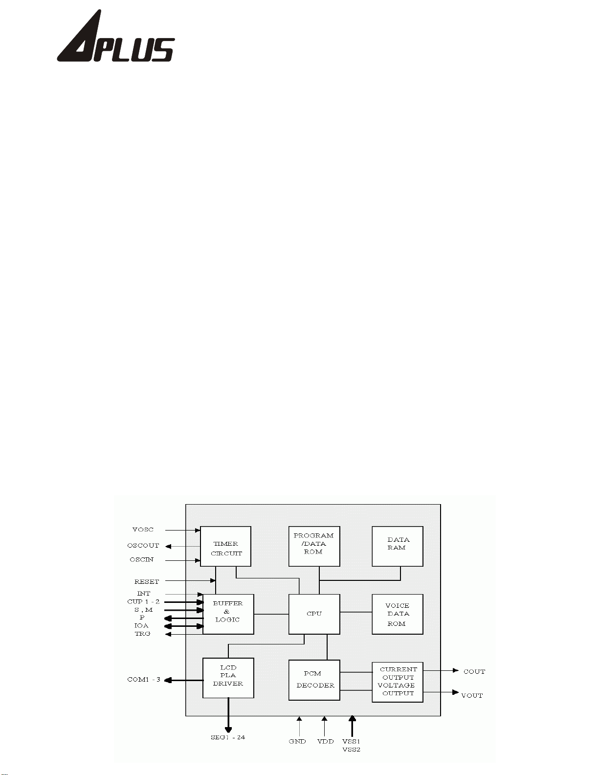
Block Diagram :
2
Rev 2.0
Page 4
AU Series
LCD Common Plate Usage:
Static 1/2 duty 1/3 duty
COM1
COM2
COM3
Alternating
frequency
Yes Yes Yes
No Yes Yes
No No Yes
32Hz 32Hz 43Hz
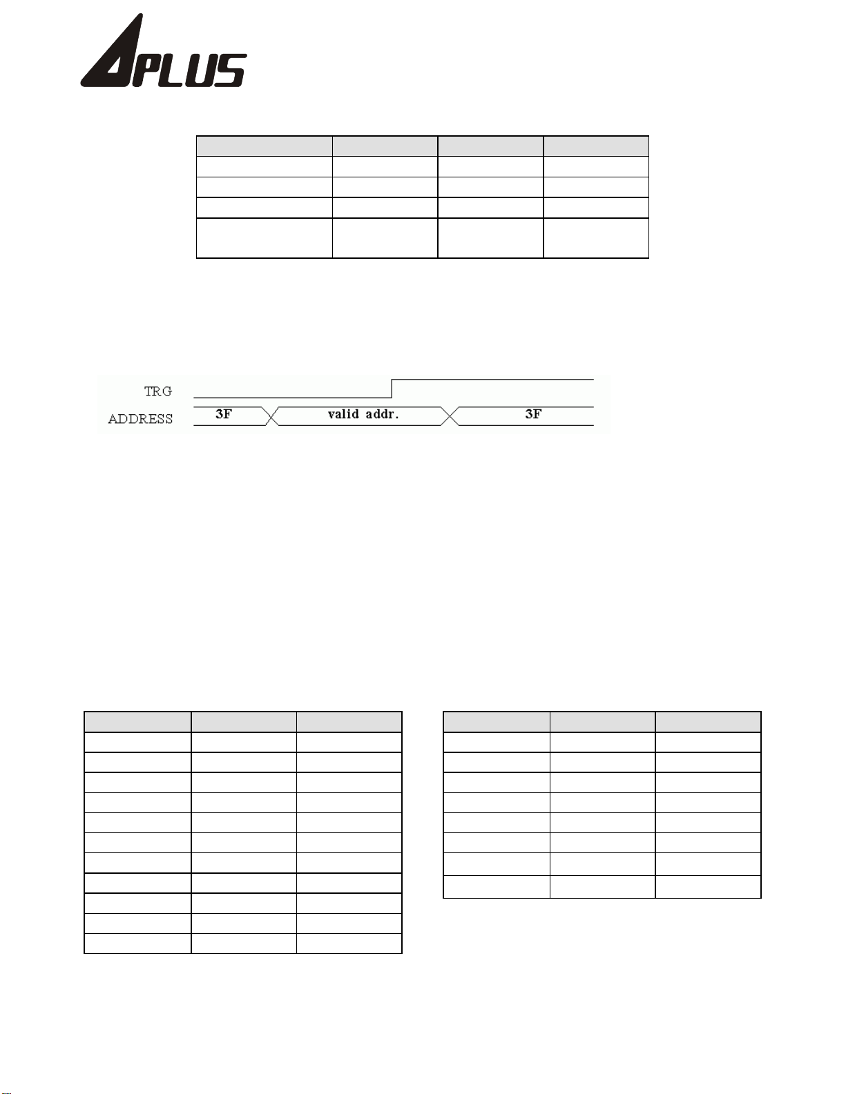
Voice Trigger:
The voice circuitry will be Triggered in the rising edge of TRG signal. The Voice section address must be placed on I/OA
and I/OB port.
(MSB) (LSB)
a) In power on state, TRG signal is reset to "LOW" level. TRG will stay at low level until the program set it to "HIGH" level.
b) Before triggering the voice circuitry, used the OIOA and OIOB instruction to place the voice section address on I/OA and
I/OB port. The voice section address couldn't be changed until the rising edge of TRG signal.
c) After triggering voice, I/OA and I/OB ports must output 3F data or set to input mode. If not, there will be a standby
current problem.
d) Example of playing voice subroutine:
Triggering the 26th(1Ah) section
LDS 3,1
LDS 4,A
OIOB 3 ; place voice section address to i/o port
OIOA 4
RF 4 ; trigger voice
SF 4
LDS 3,3
LDS 4,F
OIOA 4 ; output 3F data to I/O port
OIOB 3
I/OB2 I/OB1 I/OA4 I/OA3 I/OA2 I/OA1
Absolute Maximum Rating: (VDD=3V, VSS2=0V)
Symbol Rating Unit
VSS1 1.2-1.8 V
GND 0-0.6 V
CUP1 VSS2-VSS1 V
CUP2 VSS1-VDD V
OSCIN GND-VDD V
OSCOUT GND-VDD V
S1-S4 VSS2-VDD V
M1-M4 VSS2-VDD V
IOA1-IOA4 VSS2-VDD V
IOB1-IOB4 VSS2-VDD V
INT/BUSY VSS2-VDD V
Symbol Rating Unit
RESET VSS2-VDD V
TRG VSS2-VDD V
P1-P4 VSS2-VDD V
SEG1-24 VSS2-VDD V
COM1-3 VSS2-VDD V
VOUT1-2 VSS2-VDD V
T(operating) -10-+60
T(storage) -55-+125
℃
℃
3
Rev 2.0
Page 5

AU Series
DC Characteristics :( VDD=3V, VSS=0V )
Symbol Parameter Min. Tpy. Max. Unit Condition
VDD Operating Voltage 2.4 3 6 V
ISB Standby Current 1 uA VDD=3V, no load
IOP Operation Current uA
VOH1 Output High Voltage
(IOA, IOB, P)
VOL1 Output Low Voltage
(IOA, IOB, P)
VOH2 Output High Voltage
(TRG)
VOL2 Output Low Voltage
(TRG)
RI1 Input Resistance (S,
M)
R12 Input Resistance
(S, M)
R13 Input Resistance
3 V
0 V
3 V
0 V
1.3 Mohm
"L"-
level hold Tr.=OFF
Pull-down Tr.=ON
230 Kohm "L"-level hold Tr.=ON
Pull-down Tr.=OFF
Kohm
(INT/BUSY)
R14 Input Resistance
16.8 Kohm
(RESET)
IO1 O/P Current
VOUT1, VOUT2
ICO
O/P Current
(COUT)
-1.5 mA full scale
-3
-4.5
△F/F
Crystal Oscillator
%
Frequency Stability
△F/F
Voice Oscillator
%
Frequency Variation
4
Rev 2.0
Page 6

AU Series
Pad Description:
Pad No. Pad Name I/O Function Description
1 VDD P Positive Power supply
2-3 CUP1-2 I Voltage Halver Capacitor
4 OSCIN I Crystal Oscillator Input, 32768Hz
5 OSCOUT I Crystal Oscillator Output, 32768Hz
6 COM1 O Common plate for LCD panel
7-30 SEG1-24 O 24 segment outputs for LCD panel
31 VDD P Positive Power supply
32-33 COM2-3 O Common plate for LCD panel
34 GND G Backup negative power supply
35-36 VSS1-2 G Negative power supply
37-38 S4-3 I Input port
39 TRG I Audio output enable signal. Latch voice Section address
40-43 IOA1-4/S0-3 I/O Voice section address. Internal pull-up
44 RESET I System reset
45 VOSC I Voice oscillator input
46 COUT O Audio signal current output
47 VOUT1 O Audio signal voltage output
48 VSS2 G Negative power supply
49 VOUT2 O Audio signal voltage output
50-51 IOB1-2/S4-5 I/O Voice section address. Internal pull-up.
52-53 IOB3-4 I/O I/O port, 2 bits
54 INT/BUSY I/O Voice busy status, CPU interrupt request
55-58 P1-4 O Output port
59-62 M1-4 I Input port
63 N.C. N.C.
64-65 S2-1 I Input port
5
Rev 2.0
Page 7

AU Series
Typical Application:
※ AU1564, AU1564A has no COUT output function
6
Rev 2.0
Page 8

AU Series
Bonding Diagram:
PRODUCT X Y PAD Size ( um^2 ) Substrate UNIT
AU2064
AU2064A
AU1564
AU1564A
FOR AU2064, AU2064A:
3530 2750 85 * 85 VDD um
3050 2540 80 * 80 VDD um
7
Rev 2.0
Page 9

AU Series
FOR AU1564, AU1564A:
8
Rev 2.0
Page 10

AU Series
AU2064, AU2064A pad location
Pad No. Pad Name X Y Pad No. Pad Name X Y
1
2
3
4
5
6
7
8
9
10
11
12
13
14
15
16
17
18
19
20
21
22
23
24
25
26
27
28
29
30
31
32
33
VDD -1614.2 174.6
CUP1 -1614.2 21.6
CUP2 -1612.5 -131.4
OSCIN -1631.7 -284.4
OSCOUT -1632.6 -530.2
CON1 -1631.7 -750.9
SEG1 -1632.6 -903.9
SEG2 -1632.6 -1056.9
SEG3 -1632.6 -1209.9
SEG4 -1479.6 -1209.9
SEG5 -1335.1 -1209.9
SEG6 -1190.6 -1209.9
SEG7 -1046.1 -1209.9
SEG8 -901.6 -1209.9
SEG9 -757.1 -1209.9
SEG10 -612.6 -1209.9
SEG11 -468.1 -1209.9
SEG12 -323.6 -1209.9
SEG13 -179.1 -1209.9
SEG14 -34.6 -1209.9
SEG15 109.9 -1209.9
SEG16 254.4 -1209.9
SEG17 398.9 -1209.9
SEG18 543.4 -1209.9
SEG19 687.9 -1209.9
SEG20 832.4 -1209.9
SEG21 976.9 -1209.9
SEG22 1121.4 -1209.9
SEG23 1265.9 -1209.9
SEG24 1410.4 -1209.9
VDD 1554.9 -1209.9
COM3 1631.7 -1056.9
COM2 1631.7 -608.1
34
35
36
37
38
39
40
41
42
43
44
45
46
47
48
49
50
51
52
53
54
55
56
57
58
59
60
61
62
63
64
65
GND 1595.4 -455.1
VSS1 1601.8 -302.1
VSS2 1618.1 -149.1
S4 1631.7 3.9
S3 1631.7 190.1
TRG 1631.7 343.1
IOA1 1631.7 496.1
IOA2 1631.7 649.1
IOA3 1631.7 802.1
IOA4 1631.7 1070.2
RESET 1364.4 1216.2
VOSC 1146.8 1216.2
COUT 757.5 1216.2
VOUT1 510.7 1188.6
VSS2 339.1 1192.0
VOUT2 167.5 1188.6
IOB1 -38.5 1216.2
IOB2 -191.5 1216.2
IOB3 -344.5 1216.2
IOB4 -497.5 1216.2
INT -667.5 1216.2
P1 -820.5 1216.2
P2 -973.5 1216.2
P3 -1126.5 1216.2
P4 -1279.5 1216.2
M1 -1432.5 1216.2
M2 -1603.4 1216.2
M3 -1631.7 972.7
M4 -1631.7 819.7
TESTA -1631.7 666.7
S2 -1631.7 513.7
S1 -1631.7 327.6
9
Rev 2.0
Page 11

AU Series
AU1564, AU1564A pad location
Pad No. Pad Name X Y Pad No. Pad Name X Y
1
2
3
4
5
6
7
8
9
10
11
12
13
14
15
16
17
18
19
20
21
22
23
24
25
26
27
28
29
30
31
32
VDD -1380.6 164.3
CUP1 -1380.6 20.3
CUP2 -1379 -123.7
OSCIN -1397.16 -267.7
OSCOUT -1397.96 -496.72
COM1 -1397.16 -695.92
SEG1 -1397.96 -830.32
SEG2 -1397.96 -968.72
SEG3 -1397.96 -1127.92
SEG4 - 1273.96 -1138.72
SEG5 -1149.96 -1138.72
SEG6 -1025.96 -1138.72
SEG7 -901.96 -1138.72
SEG8 -777.96 -1138.72
SEG9 -653.96 -1138.72
SEG10 -529.96 -1138.72
SEG11 -405.96 -1138.72
SEG12 -281.96 -1138.72
SEG13 -157.96 -1138.72
SEG14 -33.96 -1138.72
SEG15 90.04 -1138.72
SEG16 214.04 -1138.72
SEG17 338.04 -1138.72
SEG18 462.04 -1138.72
SEG19 586.04 -1138.72
SEG20 710.04 -1138.72
SEG21 834.04 -1138.72
SEG22 958.04 -1138.72
SEG23 1082.04 -1138.72
SEG24 1206.04 -1138.72
VDD 1330.04 -1138.72
COM3 1397.16 -645.44
33
34
35
36
37
38
39
40
41
42
43
44
45
46
47
48
49
50
51
52
53
54
55
56
57
58
59
60
61
62
63
COM2 1397.16 -232.64
GND 1362.92 -83.84
VSS1 1369 52.16
VSS2 1384.36 188.16
S3 1397.16 357.76
TRG 1397.16 484.96
IOA1 1397.16 614.56
IOA2 1397.16 743.2
IOA3 1397.16 872.8
IOA4 1397.16 1012.8
RESET 1154.2 1144.6
VOSC 946.6 1144.6
VOUT1 692.28 1118.7
VSS2 530.76 1121.8
VOUT2 369.24 1118.7
IOB1 70.92 1144.6
IOB2 -66.68 1144.6
IOB3 -199.48 1144.6
IOB4 -337.08 1144.6
INT -491.48 1144.6
P1 -635.48 1144.6
P2 -779.48 1144.6
P3 -923.48 1144.6
P4 -1067.48 1144.6
M1 -1211.48 1144.6
M2 - 1372.36 1144.6
M3 -1397.16 915.5
M4 - 1397.16 771.5
TESTA -1397.16 627.5
S2 -1397.16 483.5
S1 -1397.16 308.3
10
Rev 2.0
Page 12

AU Series
PCB layout notice:
1. Use two lines to connect PAD1 and PAD31. The VDD line connected to PAD31 should be wider
than another one. Because PAD31 must supply the higher current.
2. Use two VSS2 lines to connect PAD36 and PAD48 (for AU1564 and AU1564A, connect PAD
36 and PAD 46). The VSS2 line connected to PAD48 (for AU1564 and AU1564A, connect
PAD 46) should be wider than another one. Because PAD48(for AU1564 and AU1564A, PAD
46) must sink the higher current.
3. Use the VDD line connected to PAD1 as the down-bond substrate.
*NOTE : all data and specification are subject to change without notice.
11
Rev 2.0
 Loading...