

Page 1
查询5962-9161301HZX供应商
PD - 94557
A TW28XXD SERIES
ADVANCED ANALOG
HYBRID-HIGH RELIABILITY
DC/DC CONVERTERS
Description
The ATW28XXD Series of DC/DC converters feature
high power density and an extended temperature range
for use in military and industrial applications. Designed
to MIL-STD-704 input requirements, these devices operate with a nominal 28 VDC inputs with ±12V and ±15V
dual outputs to satisfy a wide range of requirements.
The circuit design incorporates a pulse width modulated push-pull topology operating in the feed-forward
mode at a nominal switching frequency of 270KHz. Input
to output isolation is achieved through the use of transformers in the forward and feedback circuits.
The advanced feedback design provides fast loop response for superior line and load transient characteristics and offers greater reliability and radiation tolerance than devices incorporating optical elements in
the feedback circuits.
Three standard temperature grades are offered. Refer
to Part Number section for more severe environments.
Manufactured in a facility fully qualified to MIL-PRF38534, these converters are available in four screening grades to satisfy a wide range of requirements. The
CH grade is fully compliant to the requirements of MILPRF-38534 for class H. The HB grade is processed
and screened to the class H requirement, but may not
necessarily meet all of the other MIL-PRF-38534 requirements, e.g., element evaluation and Periodic Inspection (PI) not required. Both grades are tested to
meet the complete group “A” test specification over the
full military temperature range without output power
deration. Two grades with a more limited screening
are also available for use in less demanding applications. Variations in electr ical, mechanical and screening can be accommodated. Contact Advanced Analog
for special requirements.
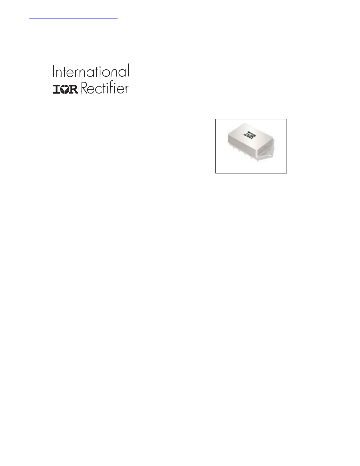
28V Input, Dual Output
ATW
Features
n 18 to 40 VDC Input Range (28 VDC Nominal)
n
±12V and ±15V Outputs Available
n Indefinite Short Circuit and Overload
Protection
n 22.8 W/in
n 30 W
n Fast Loop Response for Superior Transient
Characteristics
n Operating Temperature Range from -55°C to
+125°C Available
n Popular Industry Standard Pin-Out
n Resistance Seam Welded Case for Superior
Long Term Hermeticity
n Efficiencies up to 85%
n Shutdown from External Signal
n Full Military Screening
n 200,000 hour MTBF at 85°C
n MIL-PRF-38534 Compliant Versions
Available
3
Power Density
Output Power
www.irf.com 1
10/24/02
Page 2
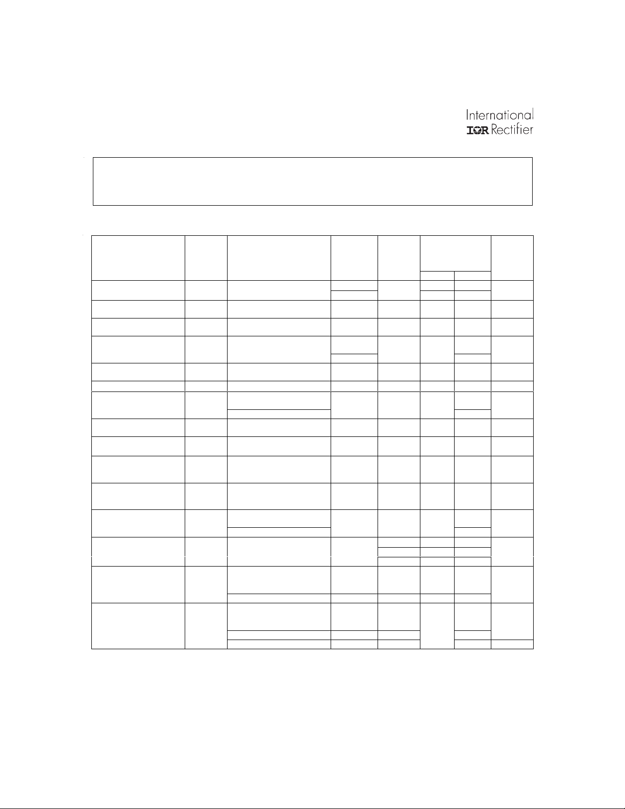
ATW28XXD Series
Specifications
ABSOLUTE MAXIMUM RATINGS
Input Voltage -0.5V to 50V
A TW2812D
Soldering Temperature 300°C for 10 seconds
Case Temperature Operating -55°C to +125°C
Storage -65°C to +135°C
T able I. Electrical P erformance Characteristics
Test Symbol Conditions
-55°C ≤Tc ≤+125°C
Vin = 28 Vdc ±5%, C
Unless otherwise specified
= 0
L
Group A
Subgroups
Min Max
Output voltage V
2,3
Output current
1, 2
Output ripple vol t ag e 3
Line regulation 4
I
OUT
VIN = 18, 28, and 40 V dc,
I
OUT
VIN = 18, 28, and 40 V dc,
V
RIP
VR
LINE
= 0 1 All
OUT
each output
B.W. = 20Hz to 2MHz
VIN = 18, 28, and 40 V dc,
Iout = 0,1250, and 2500mA
1,2,3 All 250 2250 mA
1,2,3 All 85 mVp-p
1 All 30 mV
2,3 60
VR
Load regulation 4
Cross regulation 5
Input current IIN I
I
Input ripple current
3, 4
Efficiency 4
Isolation ISO Input to output or any pin
VIN = 18, 28, and 40 V dc,
LOAD
VR
CROSS
I
I
RIP
I
E
FF
= 0, 1250, and 2500mA
I
OUT
10% to 90% load change 1,2,3 All 3.5 %
= 0, inhibit (pin 8)
OUT
tied to input return (pin 10)
= 0,inhibit (pin 8)= open 50
OUT
= 2500mA
OUT
B.W. = 20Hz to 2MHz
= 2500mA 1 All 80 %
OUT
T
= +25°C
C
1,2,3 All 120 mV
1,2,3 All 18 mA
1,2,3 All 50 mAp-p
1 All 100
to case (except pin 7) at
Capacitive load
6, 7
500 V dc Tc = +25°C
CL No effect on dc
performance, Tc = +25°C,
4 All 200 µF
total for both out put s
Power diss ip ation
load fault
Switching frequency 4
PD
I
F
S
Overload, T
Short circui t, T
= 2500mA 4,5,6 01 250 300 KHz
OUT
= +25°C 8
C
= +25°C
C
1 All 12 W
9
02 250 270
03 275 300
Output response to s tep
transient load
changes
4, 9
1250mA to/from 2500mA 4,5,6 All -400 +400 mV pk
VO
TLOAD
0mA to/from 2500mA 4,5,6 All -800 +800
Recovery time step
transient load
changes
4, 9, 10
1250mA to/from 2500mA 4,5,6 All 70 µs
TT
LOAD
0mA to/from 1250mA 4,5,6 All 500
1250mA to/from 0mA 4,5,6 All 5 ms
Device
Types
Limits Unit
11.88 ±12.12
±
11.76 ±12.24
±
V
MΩ
For Notes to Specifications, refer to page 3
2 www.irf.com
Page 3
ATW28XXD Series
T able I. Electrical P erformance Characteristics - continued
Test Symbol Conditions
-55°C ≤Tc ≤+125°C
Vin = 28 Vdc ±5%, C
unless otherwise specified
= 0
L
Group A
Subgroups
Device
Limits Unit
Types
A TW2812D
Min Max
Output response
transient step line
changes
4, 7, 11
Recovery time
transient step line
4, 7, 10, 11
change
Turn on overshoot 4
Turn on delay
4, 12
Load fault recovery 7
Input step from/to 18 to 40
VO
TLINE
Vdc, I
= 2500mA
OUT
Input step from/to 18 to 40
TT
LINE
Vdc, I
= 2500mA
OUT
VTon
I
OS
Ton
I
D
Tr
4,5,6 All 14 ms
LF
0 and 2500mA 4,5,6 All 750 mV pk
OUT =
= 0 and 2500mA
OUT
4,5,6 All -800 +800 mV pk
4,5,6 All 4000
4,5,6 All 14 ms
s
µ
Weight Flange 75 grams
Notes to Specifications
1 Parameter guaranteed by line, load and cross regulation tests.
2 Up to 90% of full power is available from either output provided the total output does not exceed 30W.
3 Bandwidth guaranteed by design. Tested for 20KHz to 2MHz.
4 Load current split equally between +V
5 Three-watt load on output under test, 3 watt to 27 watt load change on other output.
6 Capacitive load may be any value from 0 to the maximum limit without compromising dc performance.
A capacitive load in excess of the maximum limit will not disturb loop stability but may interfere with the
operation of the load fault detection circuitry, appearing as a short circuit during turn-on.
7 Parameter shall be tested as part of design characterization and after design or process changes.
Thereafter, parameters shall be guaranteed to the limits specified in Table I.
8 An overload is that condition with a load in excess of the rated load but less than that necessary to
trigger the short circuit protection and is the condition of maximum power dissipation.
9 Load step transition time between 2 and 10 microseconds.
10 Recovery time is measured from the initiation of the transient to where V
percent of V
11 Input step transition time between 2 and 10 microseconds.
at 50 percent load.
OUT
12 Tur n-on delay time measurement is for either a step application of power at the input or the removal of
ground signal from the inhibit pin (pin 8) while power is applied to the input.
OUT
and –V
OUT
.
has returned to within ±1
OUT
www.irf.com 3
Page 4

ATW28XXD Series
Specifications
ABSOLUTE MAXIMUM RATINGS
Input Voltage -0.5V to 50V
A TW2815D
Soldering Temperature 300°C for 10 seconds
Case Temperature Operating -55°C to +125°C
Storage -65°C to +135°C
T able II. Electrical P erformance Characteristics
Test Symbol Conditions
-55°C ≤Tc ≤+125°C
Vin = 28 Vdc ±5%, C
Unless otherwise specified
= 0
L
Group A
Subgroups
Device
Types
Limits Unit
Min Max
Output voltage V
I
Output current
11, 13
Output ripple voltage 8
Output Power
Line regulati o n
2,3 All 75 mV
Load regulation
4, 11
9, 10
9, 10
Input current IIN I
I
Input rippl e c urrent I
Efficiency EFF
Isolation ISO Inpu t t o output or any pin
VIN = 18, 28, and 40 Vdc 1 All
OUT
VIN = 18, 28, and 40 V dc 1,2,3 All 0.200 2000 mADC
I
OUT
V
VIN = 18, 28, and 40 V dc ,
RIP
P
OUT
VR
LINE
VR
LOAD
I
RIP
= 0 2,3 All
OUT
1,2,3 All 85 mVp-p
B.W. = DC to MHz
VIN = 18, 28, 40 Vdc 1,2,3 All 30 W
VIN = 18, 28, and 40 V dc ,
1 All 35 mV
Iout = 0, 1000, and 2000mA
VIN = 18, 28, and 40 V dc ,
= 0, 1000, and 2000mA
I
OUT
= 0, inhibit (pin 8) 1,2,3 All 12 mADC
OUT
= 0, inhibit (pin 8) = op en 1,2,3 All 30 mADC
OUT
= 2000mA 1,2,3 All 60 mAp-p
OUT
I
= 2500mA TC = 25°C
OUT
1,2,3 All 150 mV
1 All 80 %
1 All 100
14.85 ±15.15
±
14.70 ±15.30
±
V
DC
VDC
MΩ
to case (except pin 8) at
Capacitiv e l oad
6, 12
Power dissipation
load fault
Switching frequency FS I
1,2,3 02 230 245 KHz
500V dc Tc = 25°C
No effect on d c performance,
C
L
Tc = 25°C
PD
Overload, T
Short circuit, T
= 2000mA 1,2,3 01 237 263 KHz
OUT
= +25°C 3
C
= +25°C
C
4 All 500 µF
1 All 9 W
1 All 9 W
1,2,3 03 250 265 KHz
Output response to step
transient
load changes
7, 9, 10
VO
50% load t o/from 100% load 4,5,6 All - 30 0 +300 mV pk
TLOAD
No load to 100% load 4,5,6 All - 80 0 -800 mV pk
100% load to no load 4,5,6 All +800 +800 m V pk
Recovery time step
transient load changes
TT
50% load to/f r om 10 0% load 4,5,6 All 25 µs
1, 7
LOAD
No load to 50% load 4,5, 6 All 500 µs
50% load to no load 4,5,6 Al l 7 ms
For Notes to Specifications, refer to page 5
4 www.irf.com
Page 5

ATW28XXD Series
T able II. Electrical Performance Characteristics - continued
Test Symbol Conditions
-55°C ≤Tc ≤+125°C
Vin = 28 Vdc ±5%, C
unless otherwise specified
= 0
L
Group A
Subgroups
Device
Limits Unit
Types
A TW2815D
Min Max
Output response
transient step line
changes
5, 12
VO
Input step from/to 18 to
TLINE
40VDC
4,5,6 All +180 mV pk
Input step from 40 to18 VDC 4,5,6 All -600 mV pk
Recovery time
transient step line
changes
1. 5, 12
Input step from 40 to 18 VDC 4,5,6 A ll 400
Turn on overshoot VTonOS I
Turn on delay 2
Load fault recovery 12
Input step from/to 18 to 40
TT
LINE
VDC
0 and 2000mA 4,5,6 All 750 mV pk
OUT =
I
Ton
D
VIN = 18 to 40 VDC 4,5,6 All 12 ms
Tr
LF
= 0 and 2000mA
OUT
4,5,6 All 400
4,5,6 All 12 ms
s
µ
s
µ
Weight Flange 75 grams
Notes to Specifications
1 Recovery time is measured from the initiation of the transient to where V
2 Tur n-on delay time measurement is for either a step application of power at the input or the removal of a ground signal from the
inhibit pin (pin 8) while power is applied to the input.
3 An overload is that condition with a load in excess of the rated load but less than that necessary to trigger the short circuit
protection and is the condition of maximum power dissipation.
4 Above +125°C case, derate output power linearly to 0 at +135°C case.
5 Input step transition time between 2 and 10 microseconds.
6 Capacitive load may be any value from 0 to the maximum limit without compromising DC performance. A capacitive load in
excess of the maximum limit will not disturb loop stability but will interfere with the operation of the load fault detection circuitry,
appearing as a short circuit during turn on.
7 Load step transition time between 2 and 10 microseconds.
8 Bandwidth guaranteed by design. Tested for 20KHz to 2MHz.
9 Load current split equally between +V
10 When operating with unbalanced loads, at least 25% of the load must be on the positive output to maintain regulation.
11 Parameter guaranteed by line and load regulation tests.
12 Parameter shall be tested as part of design characterization and after design or process changes. Thereafter parameters shall be
guaranteed to the limits specified in Table II.
13 Up to 90% of full power is available from either output provided the total output does not exceed 30 watts.
OUT
and –V
OUT
.
has returned to within ±1% of V
OUT
at 50% load.
OUT
www.irf.com 5
Page 6

ATW28XXD Series
A TW28XXD Block Diagram
3
+Vout
1
+Input
8
Enable
2
EMI
Filter
Pulse Width
M o d u lator
Drive 1
Drive 2
FB
Sync
Input
Return
10
Application Information
Inhibit Function
Connecting the inhibit input (Pin 8) to input common (Pin 10)
will cause the converter to shut down. It is recommended
that the inhibit pin be driven by an open collector device
capable of sinking at least 400µA of current. The open circuit voltage of the inhibit input is 11.5 ±1 VDC.
EMI Filter
An optional external EMI filter (AFC461) is available that will
reduce the input ripple current to levels below the limits
imposed by MIL-STD-461B CEO3.
Device Synchronization
Whenever multiple DC/DC converters are utilized in a single
system, significant low frequency noise may be generated
due to the slight differences in the switching frequencies of
the converters (beat frequency noise). Because of the low
frequency nature of this noise (typically less than 10KHz), it
is difficult to filter out and may interfere with proper operation
of sensitive systems (communications, radar or telemetry).
Advanced Analog offers an option, which allows synchronization of multiple AHE/ATW type converters , thus eliminating this type of noise.
To take advantage of this capability, the system designer
must assign one of the converters as the master. Then, by
definition, the remaining converters become slaves and will
operate at the masters’ switching frequency.
Return
4
-Vout
5
Err o r A mp
& R e fe r e n ce
The user should be aware that the synchronization system is fail-safe; that is, the slaves will continue operating
should the master frequency be interrupted for any reason. The layout must be such that the synchronization
output (pin 2) of the master device is connected to the
synchronization input (pin 2) of each slave device. It is
advisable to keep this run short to minimize the possibility of radiating the 250KHz switching frequency.
The appropriate parts must be ordered to utilize this feature. After selecting the converters required for the system, a ‘MSTR’ suffix is added for the master converter
part number and a ‘SLV’ suffix is added for slave part
number. See Par t Number section.
T ypical Synchronization Connection
System
Bus
+ In
Return
AFC 461
or
AFV461
Output
Return
+ In
Case
Return
+ In
Case
Return
+ In
Case
Return
ATW 28xxS
ATW 28xxD
Com patable
ATW 28xxD
MSTR
or Other
SLV
SLV
Output
Return
Output
Return
Output
Output
Return
Output
6 www.irf.com
Page 7

A TW28XXD Case Outlines
0
ATW28XXD Series
1.000
0.040 D X
0.26 L Pins
123 54
4 X 0.400
=1.600
610987
0.500
Pin Designation
Pin No. Designation
1 Positive Input
2 N/C Standard or
Sync. ( Optional )
3 Positive Output
4 Output Return
5 Negative Output
6 N/C
7 Case Ground
8 Inhibit
9 N/C
10 Input Return
Enable
0.05
Max
1.95
2.360
1.350
Max
Part Numbering
ATW 28 15 D / CH - MSTR
Model
Inp ut Vo lta ge
28 = 28V Nom inal
O u tpu t Vo ltag e
Single - 05, 12, 15VDC
Dual - 12 = ±12V, 15 = ±15V
2.70
Max
Screening
–
, ES, HB, CH
Outputs
S = Single
D = Dual
Sync Option
MSTR = Master
SLV = Slave
Om it for Standard
www.irf.com 7
Page 8

ATW28XXD Series
Availab le Screening Levels and Process V ariations for A TW28XXD Series
Requirement MIL-STD-883
Temperature
Range
Element
Evaluation
Internal Visual 2017
Temperature
Cycle
Constant
Acceleration
Burn-in 1015
Final Electrical
(Group A)
Seal, Fine &
Gross
External
Visual
* Per Commercial Standards
Method
MIL-PRF-38534
1010, Cond C Cond A Yes Yes
2001, Cond A 500g 5,000g 5, 000g
MIL-PRF-38534
& Specification
1014 Yes Yes Yes
2009
No
Suffix
-20 to +85°C -55°C to +125°C -55°C to +125°C -55°C to +125°C
-55°C
∗
48hrs @ 85°C 48hrs @ 105°C 160hrs @ 125°C 160hrs @ 125°C
25°C 25°C -55, +25, +125°C -55, +25, +125°C
∗
ES
Suffix
Yes Yes Yes
Yes Yes Yes
Availab le Standard Military Drawing (SMD) Cross Reference
Standardized Vendor Vendor
Military Drawing CAGE Similar
Pin Number Pin
5962-9210901HZX 52467 ATW2812D/CH
5962-9210902HZX 52467 ATW2812D/CH-SLV
5962-9210903HZX 52467 ATW2812D/CH-MSTR
5962-9161301HZX 52467 ATW2815D/CH
5962-9161302HZX 52467 ATW2815D/CH-SLV
5962-9161303HZX 52467 ATW2815D/CH-MSTR
Code
HB
Suffix
CH
Suffix
WORLD HEADQUARTERS: 233 Kansas St., El Segundo, California 90245, Tel: (310) 322 3331
ADVANCED ANALOG: 2270 Martin Av., Santa Clara, California 95050, Tel: (408) 727-0500
Data and specifications subject to change without notice. 10/02
Visit us at www.irf.com for sales contact information.
8 www.irf.com
 Loading...