

Page 1
2 – 10 GHz Medium Power
Gallium Arsenide FET
Technical Data
ATF-46101
Features
• High Output Power:
27.0␣ dBm Typical P
• High Gain at 1 dB
Compression:
12.0␣ dB Typical G
• High Power Efficiency:
1 dB
at 4␣ GHz
1 dB
at 4␣ GHz
gate length GaAs FET is an
interdigitated four-cell structure
using airbridge interconnects
between drain fingers. Total gate
periphery is 1.25␣ millimeters.
Proven gold based metallization
systems and nitride passivation
assure a rugged, reliable device.
38% Typical at 4␣ GHz
This device is suitable for applica-
Description
The ATF-46101 is a gallium
arsenide Schottky-barrier-gate
field effect transistor designed for
medium power, linear amplification in the 2 to 10 GHz frequency
range. This nominally 0.5␣ micron
Electrical Specifications, T
Symbol Parameters and Test Conditions
P
1 dB
Power Output @ 1 dB Gain Compression: f = 4.0 GHz dBm 25.0 27.0
tions in space, airborne, military
ground and shipboard, and
commercial environments. It is
supplied in a hermetic high
reliability package with low
parasitic reactance and minimum
thermal resistance.
= 25° C
A
[1]
VDS = 9 V, IDS = 125 mA f = 8.0 GHz 26.5
G
1 dB
1 dB Compressed Gain: VDS = 9 V, IDS = 125 mA f = 4.0 GHz dB 9.0 10.0
f = 8.0 GHz 5.0
η
add
g
m
I
DSS
V
P
Note:
1. RF Performance is determined by packaging and testing 10 samples per wafer.
Efficiency @ P
1dB
: V
= 9 V, I
DS
= 125 mA f = 4.0 GHz % 38
DS
Transconductance: VDS = 2.5 V, IDS = 125 mA mmho 100
Saturated Drain Current: VDS = 2.5 V, VGS = 0 V m A 200 330 450
Pinch-off Voltage: VDS = 2.5 V, IDS = 5 mA V -5.4 -3.5 -2.0
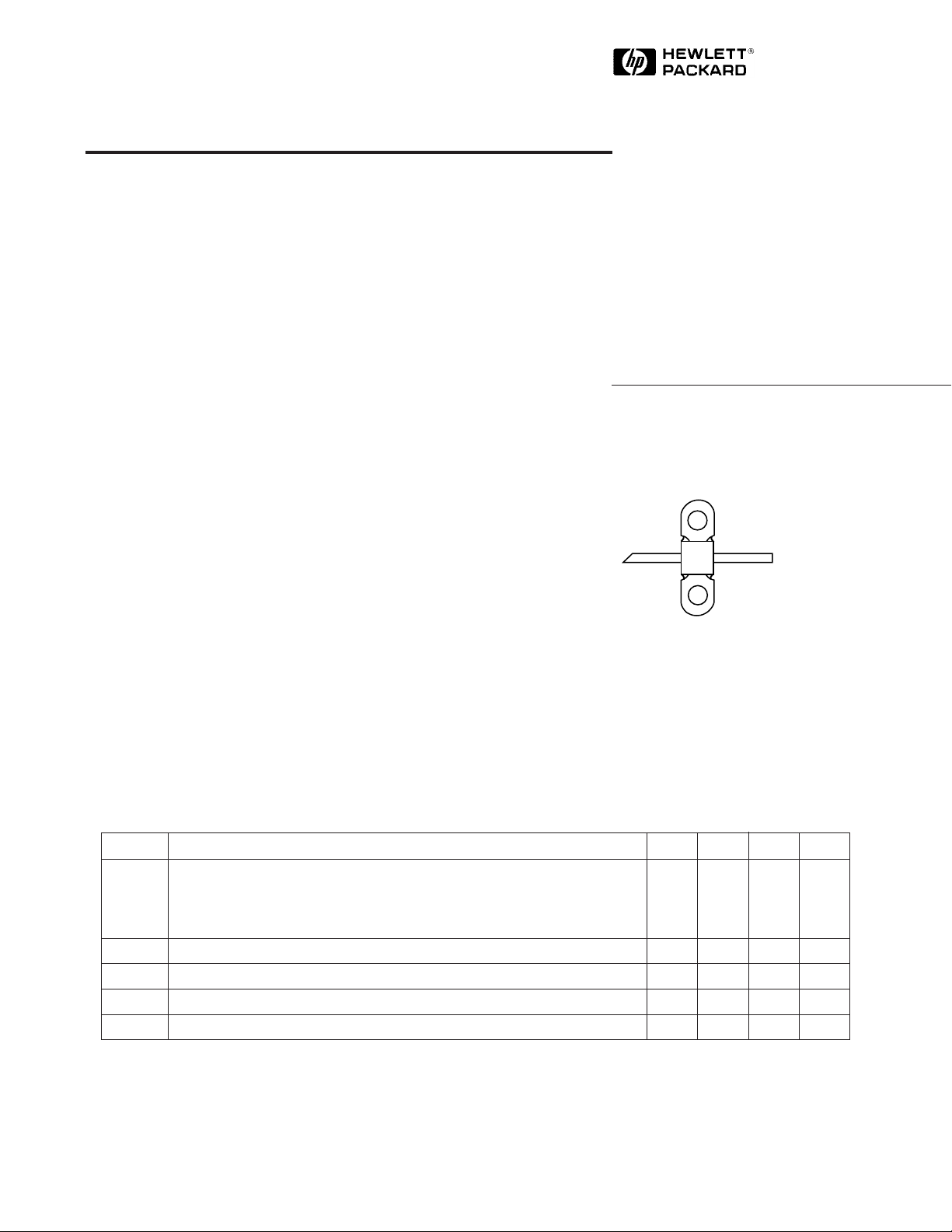
100 mil Flange Package
Units Min. Typ. Max.
5965-8731E
5-98
Page 2
ATF-46101 Absolute Maximum Ratings
Absolute
Symbol Parameter Units Maximum
V
DS
V
GS
V
GD
I
DS
P
T
T
CH
T
STG
Thermal Resistance: θjc = 75°C/W; T
Liquid Crystal Measurement: 1␣ µm Spot Size
Drain-Source Voltage V +14
Gate-Source Voltage V -7
Gate-Drain Voltage V -16
Drain Current mA I
Power Dissipation
[2,3]
W 2.0
Channel Temperature °C 175
Storage Temperature °C -65 to +175
= 150°C
CH
[4]
DSS
[1]
Notes:
1. Permanent damage may occur if
any of these limits are exceeded.
2. T
MOUNTING SURFACE
= 25° C.
3. Derate at 13 mW/° C for
> 25°C.
T
CASE
4. The small spot size of this technique results in a higher, though
more accurate determination of θ
than do alternate methods. See
MEASUREMENTS section for
more information.
jc
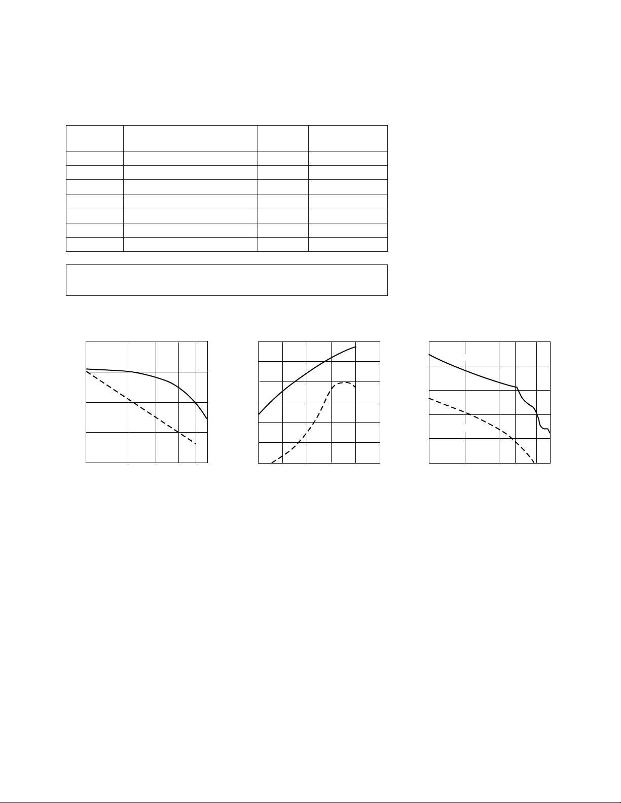
ATF-46101 Typical Performance, T
28
P
27
(dBm)
26
1 dB
P
25
24
2.0 6.04.0 8.0 10.0 12.0
1 dB
G
1 dB
FREQUENCY (GHz)
Figure 1. Power Output @ 1 dB Gain
Compression and 1 dB Compressed
Gain vs. Frequency.
VDS = 9V, IDS = 125 mA.
20
15
10
5
0
30
25
20
15
(dBm)
(dBm)
OUT
1 dB
P
G
10
5
0
0 5 10 15
Figure 2. Output Power and Power
Added Efficiency vs. Input Power.
VDS = 9 V, IDS = 125 mA, f = 4.0 GHz.
= 25° C
A
PIN (dBm)
20 25
25
20
40
30
20
10
0
15
10
GAIN (dB)
(%)
add
5
η
0
1.0 2.0 4.0 6.0
MSG
2
|S21|
FREQUENCY (GHz)
Figure 3. Insertion Power Gain,
Maximum Available Gain and
Maximum Stable Gain vs. Frequency.
VDS = 9 V, IDS = 125 mA.
MAG
MAG
14.010.0
5-99
Page 3

Typical Scattering Parameters, Common Emitter, Z
Freq. S
11
S
21
= 50 Ω, TA=25°C, V
O
S
12
=9 V, I
DS
=␣ 125 mA
DS␣
S
GHz Mag. Ang. dB Mag. Ang. dB Mag. Ang. Mag. Ang.
1.0 .94 -56 12.8 4.37 135 -31.4 .027 52 .64 -28
2.0 .86 -101 10.7 3.41 98 -27.3 .043 30 .59 -56
3.0 .82 -131 8.4 2.64 71 -26.9 .045 18 .58 -79
4.0 .82 -152 6.7 2.16 48 -26.4 .048 9 .62 -98
5.0 .80 -173 5.4 1.86 26 -26.0 .050 -1 .63 -112
6.0 .79 165 4.3 1.64 5 -25.8 .051 -12 .65 -126
7.0 .78 143 3.1 1.43 -18 -25.4 .054 -24 .65 -145
8.0 .78 131 1.6 1.20 -36 -24.7 .058 -37 .70 -166
9.0 .77 123 0.3 1.03 -55 -23.9 .064 -40 .73 173
10.0 .76 118 -1.2 .87 -72 -23.1 .070 -52 .76 158
11.0 .67 104 -2.0 .79 -91 -22.6 .074 -57 .79 146
12.0 .60 86 -2.7 .73 -110 -21.2 .087 -66 .83 136
13.0 .54 71 -3.5 .67 -133 -19.7 .104 -79 .87 124
14.0 .50 64 -4.0 .63 -154 -15.9 .160 -99 .92 115
A model for this device is available in the DEVICE MODELS section.
100 mil Flange Package Dimensions
.05
R, TYP
1.3
SOURCE
DRAIN
.062 DIA.
1.57 (2) PLCS
SOURCE
.12
3.0
3
.03
0.8
.42
10.7
.265
6.73
4
GATE
1
2
0.025 ± 0.003 mils
0.64 ± 0.08 mm
22
.044
1.12
.06
1.6
Package marking code is 461
.100
2.54
.300 min
Notes:
(unless otherwise specified)
1. Dimensions are
2. Tolerances
in .xxx = ± 0.005
mm .xx = ± 0.13
in
mm
.004 ± .002
.10 ± .05
5-100
 Loading...