

Datasheet ATF1500ABV-12JC, ATF1500ABV-12AC, ATF1500ABVL-25JC, ATF1500ABVL-25AC, ATF1500ABV-15JI Datasheet (ATMEL)
...Page 1
Features
Operates Between 2.7V to 5.5V
•
High Density, High-Performance Electrically Erasable Complex
•
Programmable Logic Device
– 44-Pin, 32 I/O CPLD
– 12 ns Maximum Pin-to-Pin Delay
– Registered Operation Up To 90.9 MHz
– Fully Connected Input and Feedback Logic Array
Flexible Logic Macrocell
•
– D/T/Latch Configurable Flip Flops
– Global and Individual Register Control Signals
– Global and Individual Output Enable
– Programmable Output Slew Rate
Advanced Power Management Features
•
– Automatic 3 mA Stand-By (ATF1500ABVL)
– Pin-Controlled 5
– Programmable Pin-Keeper Inputs and I/Os
Available in Commercial and Industrial Temperature Ranges
•
Available in 44-Pin PLCC and TQFP Pack ages
•
Advanced Flash Technology
•
– 100% Tested
– Completely Reprogrammable
– 100 Program/Erase Cyc le s
– 20 Year Data Retention
– 2000V ESD Protection
– 200 mA Latch-Up Immunity
Supported By Popular 3rd Party Tools
•
Security Fuse Feature
•
µµµµ
A Stand-By Mode (Typical)
HighPerformance
EE PLD
ATF1500ABV
ATF1500ABVL
ATF1500ABV/L
Description
The ATF1500ABV is a hi gh performance , high density Co mplex PLD. Built on an
advanced Flash technology, it has maximum pin to pin delays of 12 ns and supports
sequential logic ope ration at speeds up to 90.9 MHz. With 32 logic macr oce lls a nd u p
to 36 inputs, it easily integrates logic from several TTL, SS I, MSI and classic PLDs.
The ATF1500ABV’s global input a nd feedb ack arc hitectur e simpli fies logic pla cemen t
and eliminates pinout changes due to design changes.
(continued)
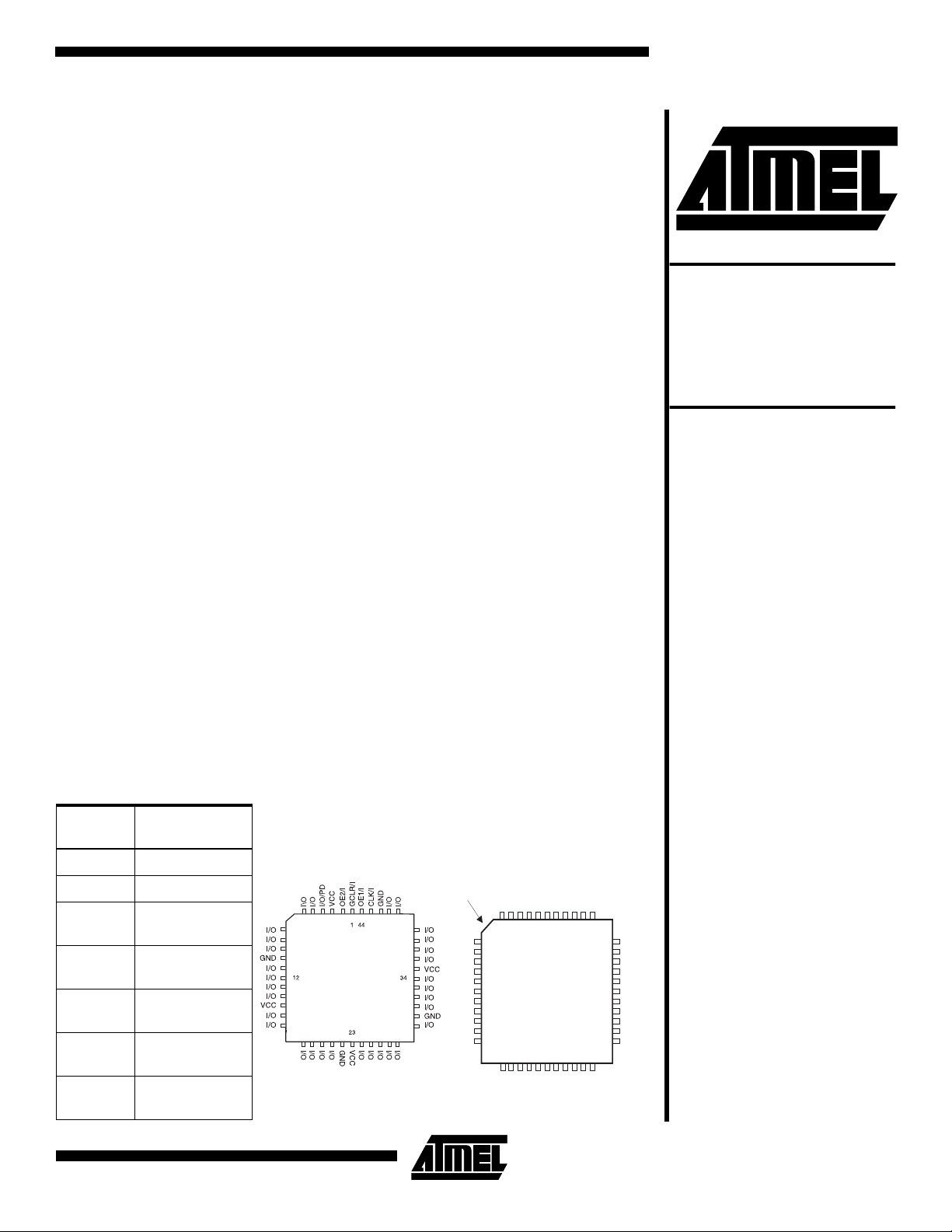
Pin Configurations
44
1
2
3
4
5
6
7
8
9
10
11
12
TQFP
Top View
VCC
I/O
I/O
I/O/PD
424340
41
15
13
14
I/O
I/O
I/O
I/O
16
GCLR/I
OE2/I
39
17
VCC
GND
OE1/I
38
18
I/O
CLK/I
GND
36
37
192021
I/O
I/O
I/O
I/O
34
35
I/O
33
I/O
32
I/O
31
I/O
30
29
VCC
I/O
28
I/O
27
I/O
26
I/O
25
GND
24
I/O
23
22
I/O
I/O
Pin
Name Function
CLK Clock
I Logic Inputs
I/O
GCLR
OE1,
OE2
V
CC
PD
Bidirectional
Buffers
Register Reset
(active low)
Output Enable
(active low)
(+3V to 5.25V)
Supply
Power Down
(active high)
PLCC
Top View
INDEX
CORNER
I/O
I/O
I/O
GND
I/O
I/O
I/O
I/O
VCC
I/O
I/O
Rev. 0723D–6/98
1
Page 2
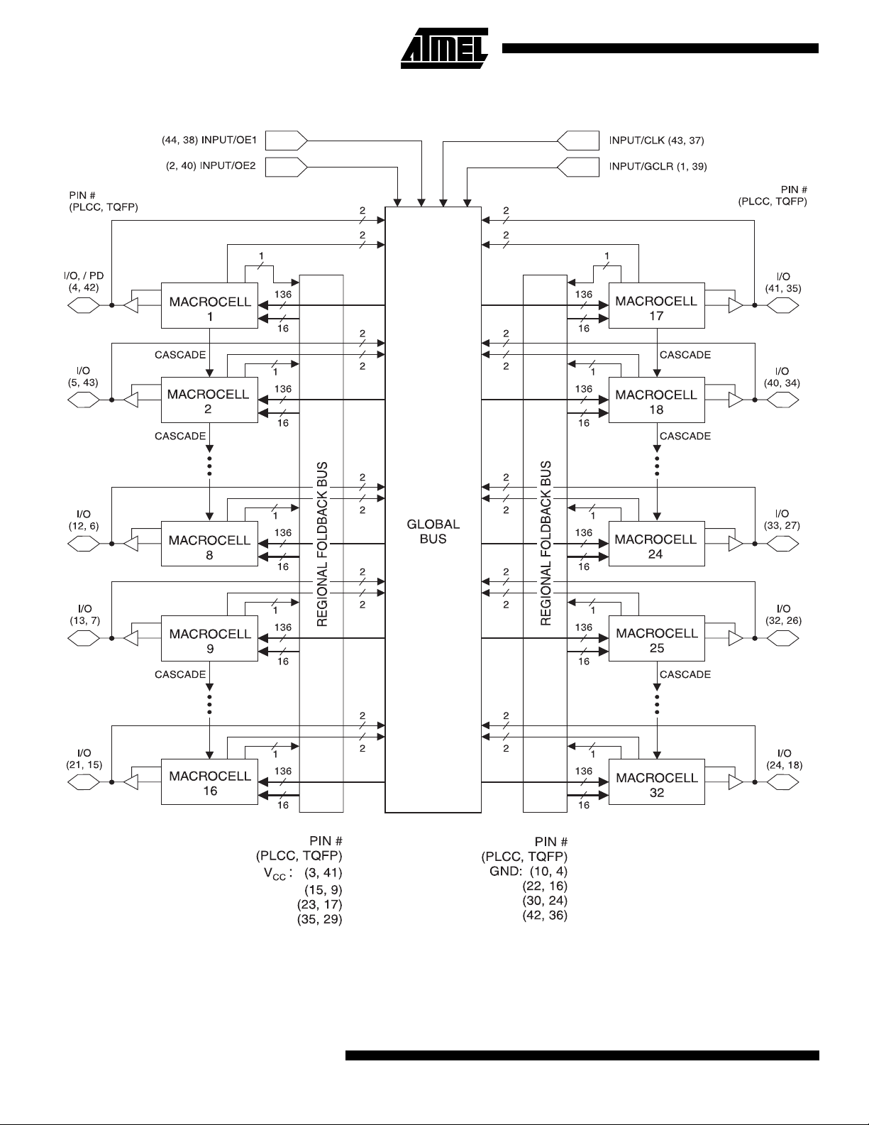
Functional Logic Diagram
(1)
Note: 1. Arrows connecting macrocells indicate direction and groupings of CASIN/CASOUT data flow.
2
ATF1500ABV/L
Page 3
ATF1500ABV/L
The ATF1500ABV has 32 bi-directional I/O pins and 4 dedicated input pins. Each dedicated input pin can also serve
as a global control signal: register clock, register reset or
output enable. Each of these control signals can be
selected for use individually within each macrocell.
Each of the 32 logic macrocells generates a buried feedback, which goes to th e global bus. Each in put and I/O pin
also feeds into the global bus. Because of this global bussing, each of these signals is always available to all 32
macrocells in the device.
Each macrocell also generates a foldback logic term, which
goes to a regional b us . Al l s i gnal s with in a r egional bus are
connected to all 16 macrocells within the region.
Cascade logic between macrocells in the ATF1500ABV
allows fast, efficient generation of complex logic functions.
The ATF1500AB V contains 4 such log ic chains, each
capable of creatin g sum te rm lo gic wi th a fan in of up to 40
product terms.
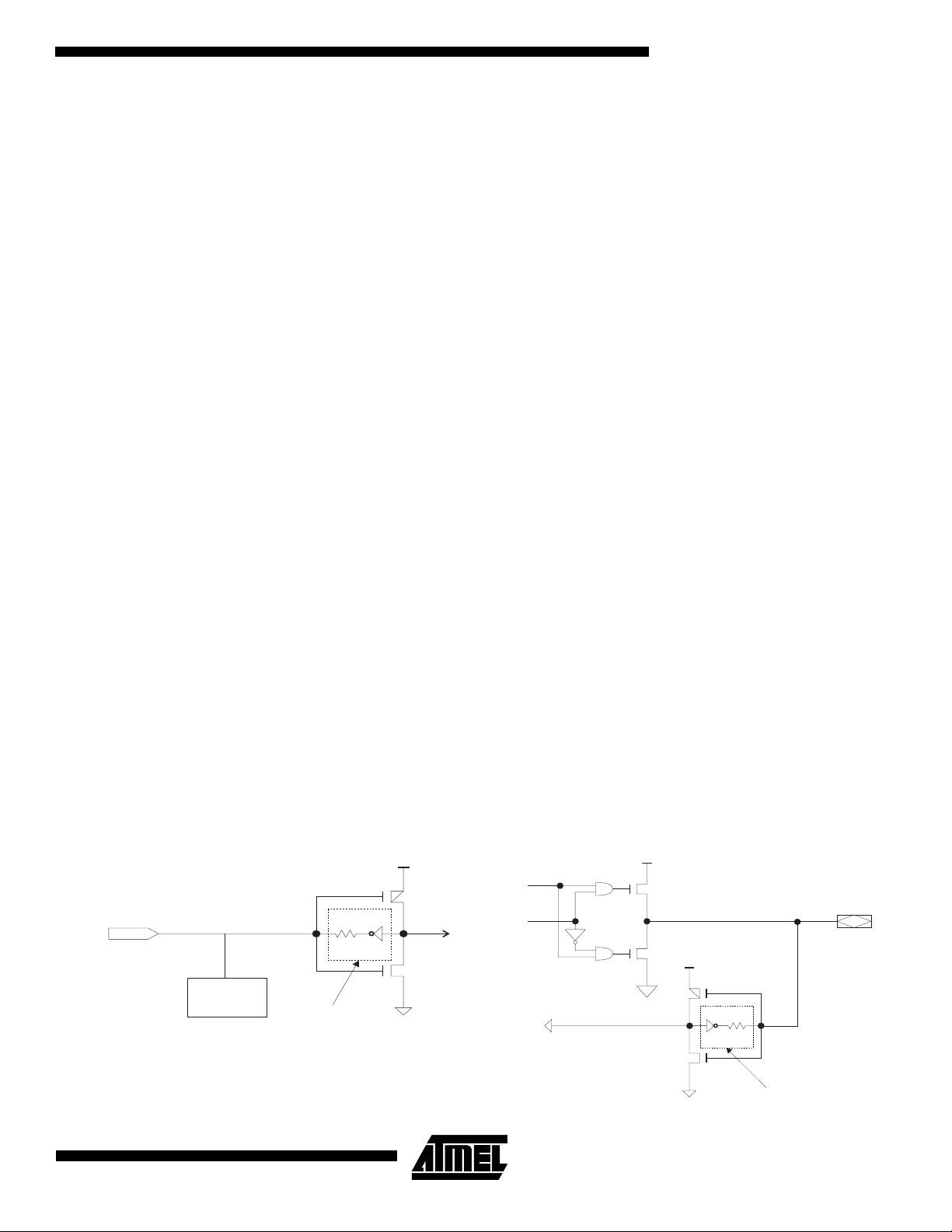
Bus Friendly Pin-Keeper Input and
I/O’S
All Input and I/O pins on the ATF1500ABV have programmable “data keeper” circui ts. If activated, when any pi n is
driven high or low and t hen su bsequently left floating, it will
stay at that previous high or low level.
This circuitry prevents un used Input and I/O lines from
floating to inter mediat e volt age leve ls, whic h caus e unnecessary power consumption and system noise. The keeper
circuits eliminate the need for external pull-up resistors and
eliminate their DC power consumption.
Pin-keeper circuits c an be di sabled. Pr ogramming is co ntrolled in the logic design file. Once the pin-keeper circuits
are disabled, normal termination procedures are required
for unused inputs and I/Os.
Speed/Power Management
The ATF1500ABV has several built-in s peed and power
management features. The ATF1500ABV contains circuitry
that automatically puts the device into a low power standby mode when no logic trans itions are oc curring. This not
only reduces power consumption during inactive periods,
but also prov ides a p roportion al power savings for most
applications running at system speeds below 10 MHz.
All ATF1500AB Vs also have an op tional pin-contr olled
power down mode. In this mod e, c urre nt d rops to b elo w 10
µA. When the power down op tion i s sel ec ted , the P D pi n i s
used to power down the part. The power down option is
selected in the design source file. When enab led, the
device goes into power down wh en the PD pin i s high. In
the power down mode, all internal logic signal s are latched
and held, as are any enabled outputs. All pin transitions are
ignored until the PD is brou ght low. W hen the po wer down
feature is ena bled, the PD c annot be used as a logi c inp ut
or output. However, the PD pin's macrocell may still be
used to generate buried foldb ack and cascade log ic signals.
Each output also has individual slew rate control. This may
be used to reduce system noise by slowing down outputs
that do not need to operate at maximum speed. Outputs
default to slow switching, and may be specified as fast
switching in the design file.
Design Software Support
ATF1500ABV designs are support ed by several 3rd party
tools. Automated fitters allow logic synthesis using a variety
of high level description languages and formats.
Input Diagram
INPUT
ESD
PROTECTION
CIRCUIT
100K
PROGRAMMABLE
OPTION
I/O Diagram
V
V
CC
OE
DATA
CC
I/O
V
CC
100K
PROGRAMMABLE
OPTION
3
Page 4
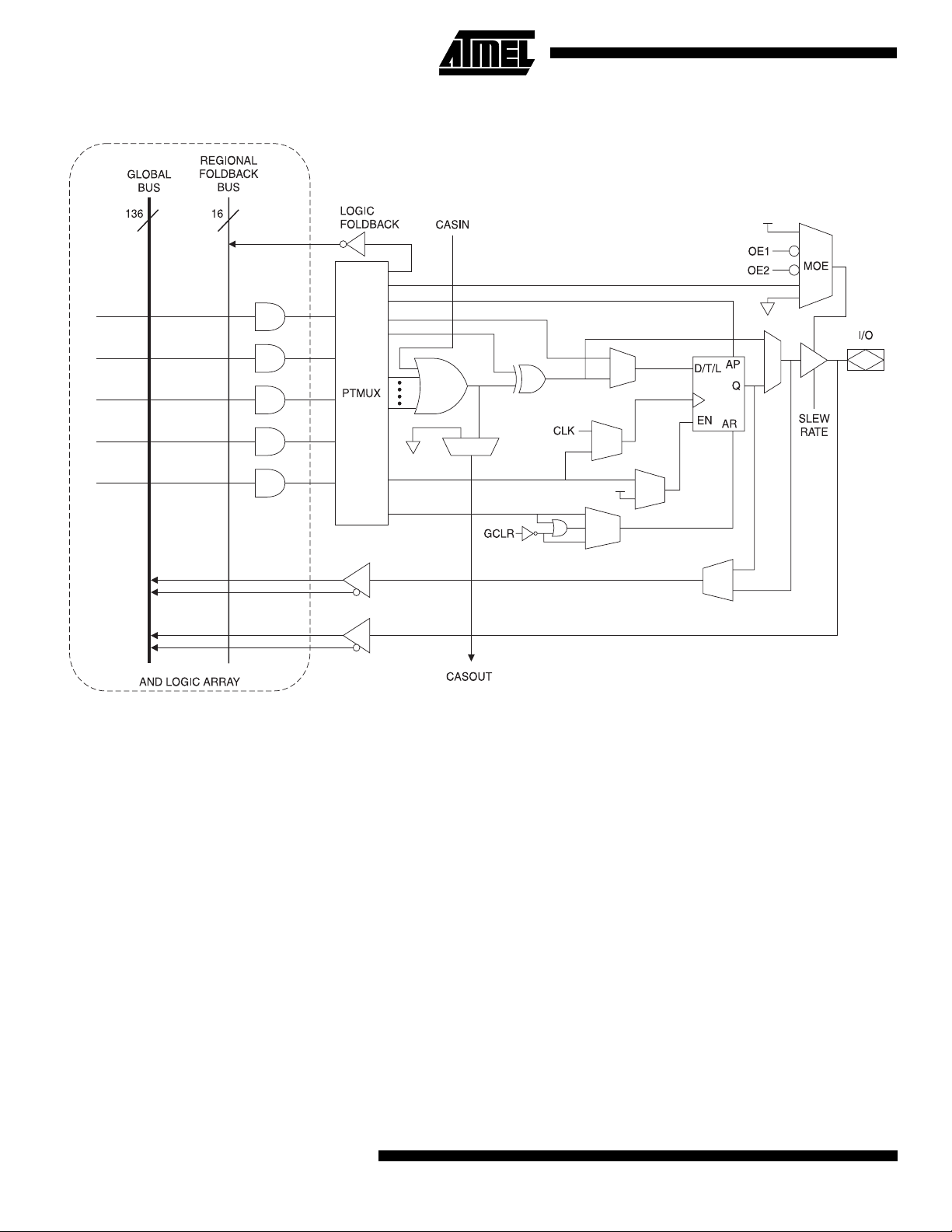
ATF1500ABV Macrocell
ATF1500ABV Macrocell
The ATF1500ABV macrocell is flexib le enough to su pport
highly complex logi c functions operating at high speed. The
macrocell consists of five sections: product terms and product term select multiplex er; OR/XOR/CASCADE logic; a flip
flop; output select and enable; and logic array inputs.
Product Terms and Select Mux
Each ATF1500ABV macrocell has five product terms. Each
product term recei v es as its i nputs all signals from both the
global bus and regional bus.
The product term selec t multi plex er (PTMU X) allo cates the
five product terms as needed to the macrocel l logic g ates
and control signals. The PTMUX programming is determined by the design compiler, wh ich sel ects the opti mum
macrocell configuration.
OR/XOR/CASCADE Logic
The ATF1500ABV macrocell's OR/XOR/CASCADE l ogic
structure is designed to efficiently support all types of logic.
Within a single mac rocell, all the product terms can be
routed to the OR gate, creating a five input AND/OR sum
4
ATF1500ABV/L
term. With the addition of the CASIN from neighboring
macrocells, this can be expanded to as many as 40 product
terms with a very small additional delay.
The macrocell's XOR gate allows efficient implementation
of compare and arithmeti c function s. One inpu t to the XOR
comes from the OR sum term. The other XOR input can be
a product term or a fixed high or low level. For combinatorial outputs, the fixed level input allows output polarity
selection. For regi stered functions, the fixed levels allow De
Morgan minimization of the product terms. The XOR gate is
also used to emulate JK type flip flops.
Flip Flop
The ATF1500ABV’s flip fl op has very flexible data and control functions. The data input can come from either the XOR
gate or from a separate product term. Selecting the separate product term allows creation of a buried registered
feedback within a combinatorial output macrocell.
In addition to D, T, JK and SR operation, the flip flop can
also be configured as a flow-through latch. In this mode,
Page 5

ATF1500ABV/L
data passes through when the clock is high and is latched
when the clock is low.
The clock itself ca n be eit her the gl obal CL K pin or an indi vidual prod uct term. The flip flop chan ges stat e on the
clock's rising edge. When the CLK pin is used as the clock,
one of the macrocell product terms can be selected as a
clock enable. W hen the clock enab le fu nctio n is act ive and
the enable sign al (prod uct ter m) is lo w, all cloc k edge s are
ignored.
The flip flop's asynchronous reset signal (AR) can be either
the pin global clear (GCLR), a product term, or always off.
AR can also be a logic O R of GCLR with a p roduct te rm.
The asynchronous preset (AP) can be a product term or
always off.
Output Select and Enable
The ATF1500ABV macrocell output can be selected as
registered or combinatorial. When the output is registered,
the same registered si gnal is fed bac k interna lly to the global bus. When the output i s combi nator ial, th e buried feedback can be either the same combinatorial signal or it can
be the register output if the separate pro duct term is chosen as the flip flop input.
The output enable multiplexer (MOE) controls the output
enable signals. Any buf fer can be pe rmanen tly enabled for
simple output operation. Buffers c an also be permanently
disabled to allow use of the pin as an input. In thi s con figuration all the macroc ell reso urces are still avai lable, in cluding the buried feedback, expander and CASCADE logic.
The output enable for eac h mac rocell can also be s elect ed
as either of the two OE pins or as an individual product
term.
Global/Regional Busses
The global bus contains all Input and I/O pin signals as well
as the buried feed back signal from al l 32 macrocells.
Together with the complemen t of eac h s ign al, t his pr ov id es
a 68-bit bus as input to every product term. Having the
entire global bus available to each macrocell eliminates any
potential rout ing prob lems. With this arch itecture d esigns
can be modified without requiring pinout changes.
Each macrocell also generat es a foldback product term.
This signal goes to the regi onal bus , and is a vailabl e to 16
macrocells. The foldback is an inverse polarity of one of the
macrocell's product terms. T he 16 foldb ack terms in ea ch
region allow generation of high fan-in sum terms (up to 21
product terms) with a small additional delay.
5
Page 6

Absolute Maximum Ratings*
Temperature Under Bias................................ -55°C to +125°C
Storage Temperature..................................... -65°C to +150°C
Voltage on Any Pin with
Respect to Ground .......................................-2.0V to +5.25V
(1)
Voltage on Input Pins
with Respect to Ground
During Programming.....................................-2.0V to +14.0V
Programming Voltage with
Respect to Ground .......................................-2.0V to +14.0V
(1)
(1)
*NOTICE: Stresses beyond those listed under “Absolute
Maximum Ratings” may cause permanent damage to the dev ice . This is a s tress rating only an d
functional oper ation of the device at these o r any
other conditions beyond those indicated in the
operational sections of this specification is not
implied. Exposure to absolute maximum rating
conditions f or e xtended periods ma y af fect de vice
reliability.
Note: 1. Minimum voltage is -0.6V dc, which may under-
shoot to -2.0V for pulses of less than 20 ns. Maximum out put pin voltage is V
which may overshoot to 5.25V for pulses of less
than 20 ns.
DC and AC Operating Conditions
Commercial Industrial
Operating Temperature (Case) 0°C - 70°C -40°C - 85°C
V
Power Supply 2.7V - 5.5V 2.7V - 5.5V
CC
+ 0.75V dc,
CC
DC Characteristics
Symbol Parameter Condition Min Typ Max Units
I
IL
I
IH
(1)
I
CC1
I
CC2
I
OS
V
IL
V
IH
V
OL
V
OH
Note: 1. All ICC parameters measured with outputs open, and a 16 bit loadable, up/down counter programmed into each region.
Input or I/O
Low Leakage Current
Input or I/O
High Leakage Current
0 ≤ VIN ≤ VIL(max) -10 µA
,min < VIN ≤ V
V
IH
CC
10 µA
Com. 35 mA
ATF1500ABV
Power Supply Current,
Standby
VCC = MAX,
= 0, V
V
IN
CC
Ind. 40 mA
Com. 3 mA
ATF1500ABVL
Ind. 5 mA
Power Supply Current,
Power Down Mode
Output Short Circuit
Current
Input Low Voltage
= MAX,
V
CC
= 0, V
V
IN
V
OUT
VCC, min < VCC
< V
CC
= 0.5V -130 mA
CC
, max
-0.5 0.8 V
2mA
Input High Voltage 2.0 VCC + 1 V
Output Low Voltage VCC = MIN IOL = 4 mA 0.45 V
Output High Voltage VCC = MIN IOH = -0.1 mA VCC - .2 V
6
ATF1500ABV/L
Page 7

AC Waveforms
ATF1500ABV/L
Register AC Characteristics, Input Pin Clock
(1)
Symbol Parameter 2.7-volt Adder
(2)
t
COS
t
CFS
t
SIS
t
SFS
t
HS
t
PS
t
WS
F
MAXS
t
RPRS
t
RTRS
Clock to Output .5 2728 ns
Clock to Feedback 033ns
I, I/O Setup Time 11011ns
Feedback Setup Time 11011ns
Input, I/O, Feedback Hold Time 00 0 ns
Clock Period 113 14 ns
Clock Width .5 6.5 7 ns
External Feedback 1/(t
Internal Feedback 1/(t
No Feedback 1/(t
PS
+ t
SIS
SFS
) -5 58.8 52.6 MHz
COS
+ t
) -5.5 76.9 71.4 MHz
CFS
) -5.5 76.9 71.4 MHz
Reset Pin Recovery Time 13 4 ns
Reset Term Recovery Time 110 12 ns
Notes: 1. AC Characteristics are for VCC = 3.0 volts. For 2.7 volts, add the "2.7-volt adder."
2. For slow slew outputs, add t
SSO
.
-12 -15
UnitsMinMaxMinMax
= Preliminary Information
7
Page 8

Register AC Characteristics, Product Term Clock
(1)
-12 -15
Symbol Parameter 2.7-volt Adder
(2)
t
COA
t
CFA
t
SIA
t
SFA
t
HA
t
PA
Clock to Output 21215ns
Clock to Feedback 1 8 10 ns
I, I/O Setup Time 04 4 ns
Feedback Setup Time 04 4 ns
Input, I/O, Feedback Hold Time 04 4 ns
Clock Period 112 14 ns
UnitsMin Max Min Max
tWAClock Width .5 6 7 ns
F
MAXA
t
RPRA
t
RTRA
External Feedback 1/(t
Internal Feedback 1/(t
No Feedback 1/(t
PA
Reset Pin Recovery Time 00 0 ns
Reset/Preset Term Recovery Time 06 6 ns
+ t
SIA
SFA
) -7 62.5 52.6 MHz
COA
+ t
) -6.4 83.3 71.4 MHz
CFA
) -6.4 83.3 71.4 MHz
Notes: 1. AC Characteristics are for VCC = 3.0 volts. For 2.7 volts, add the “2.7-volt Adder.”
2. For slow slew outputs, add t
SSO .
AC Characteristic
-12 -15
Symbol Parameter 2.7-volt Adder
(2)
t
PD
t
PD2
(2)
t
PD3
t
PD4
(2)
t
EA
I, I/O or FB to Non-Registered Output 2312315ns
I, I/O to Feedback 189ns
Feedback to Non-Registered Output 2312315ns
Feedback to Feedback 189ns
OE Term to Output Enable 1312315ns
tEROE Term to Output Disable 1212215ns
(2)
t
PZX
t
PXZ
t
PF
(2)
t
PO
t
RPF
(2)
t
RPO
t
RTF
(2)
t
RTO
t
CAS
t
SSO
t
FLD
OE Pin to Output Enable 12829ns
OE Pin to Output Disable 1 1.581.59 ns
Preset To Feedback 1912ns
Preset to Registered Output 21420ns
Reset Pin to Feedback 135ns
Reset Pin to Registered Output 1811ns
Reset Term to Feedback 1912ns
Reset Term to Registered Output 21420ns
Cascade Logic Delay 011ns
Slow Slew Output Adder 034ns
Foldback Term Delay 178ns
Notes: 1. AC Characteristics are for VCC = 3.0 volts. For 2.7 volts, add the “2.7-volt Adder.”
2. For slow slew outputs, add t
8
ATF1500ABV/L
SSO
.
= Preliminary Information
UnitsMin Max Min Max
Page 9

ATF1500ABV/L
P ower Down AC Characteristics
(1)
Symbol Parameter 2.7-volt Adder
t
IVDH
t
GVDH
t
CVDH
t
DHIX
t
DHGX
tDHCX Clock Don't Care After PD High
t
DLIV
t
DLGV
t
DLCV
(1)
t
DLOV
Valid I, I/O Before PD High 112 15 ns
Valid OE
Valid Clock
(3)
Before PD High 112 15 ns
(3)
Before PD High 112 15 ns
Input Don't Care After PD High 122 25 ns
OE Don't Care After PD High 122 25 ns
122 25 ns
PD Low to Valid I, I/O 011µs
PD Low to Valid OE
PD Low to Valid Clock
(3)
(3)
011µs
011µs
PD Low to Valid Output 011µs
Notes: 1. AC Characteristics are for VCC = 3.0 volts. For 2.7 volts, add the “2.7-volt Adder.”
2. For slow slew outputs, add t
SSO
.
3. Pin or Product Term.
Input Test Waveforms and
Output Test Load
Measurement Levels
-12 -15
UnitsMinMaxMinMax
= Preliminary Information
Pin Capacitance
(f = 1 MHz, T = 25°C)
C
IN
C
OUT
Note: 1. Typical values for nominal supply voltage. This parameter is only sampled and is not 100% tested.
(1)
Typ Max Units Conditions
4.5 5.5 pF VIN = 0V
3.5 4.5 pF V
OUT
= 0V
9
Page 10

Power Up Reset
The ATF1500ABV’s registers are designed to reset during
power up. At a point delayed slightly from V
, all registers will be reset to the low sta te. As a res ult,
V
RST
crossing
CC
the registered output state will always be low on power-up.
This feature is critical for state machine initialization. How-
ever, due to the asynchronous nature of reset and the
uncertainty of how V
actually rises in the sy stem, the fol -
CC
lowing conditions are required:
1. The V
rise must be monotonic, from below .7
CC
volts.
2. Signals from which clocks are derived must remain
stable during T
3. After T
occurs, all input and feedbac k setup times
PR
PR
.
must be met before driving the cloc k signal high.
Power Down Mode
The ATF1500ABV includes an optional pin controlled
power down feature. When this mode is enabled, the PD
pin acts as the power down pin. When the PD pin is high,
the device supply cur rent is reduced to less than 1 0 µA.
During power down, all output data and internal logic states
are latched and held. Therefore, all registered and combinatorial output data remain valid. Any outputs which were
in a HI-Z state at the onset of power down will remain at HIZ. During power do wn, all inpu t signals ex cept the powe r
down pin are blocked. Input and I/O hold latches remain
active to insure that pins do not float to indeterminate levels, further reducing system power. The power down pin
feature is enabled in the logic design file. Designs using the
power down pin may not use the PD pin l ogic array input.
However, all other PD pin macrocell resources may still be
used, including the buried feedb ack and foldback produc t
term array inputs.
Register Preload
The ATF1500ABV’s registers are provided with circuitry to
allow loading of each register with either a high or a low.
This feature will simplify testing since any state c an be
forced into the register s to control test s equencing. A
JEDEC file with pr eload is gen erated when a sou rce file
with preload vectors is c ompiled. Once downl oaded, the
JEDEC file preload seque nce will be don e automatically
when vectors are run by any approved programmers. The
preload mode is ena bled by raising an input pin to a high
voltage level. Contact Atmel PLD Applications for PRELOAD pin assignments, timing and voltage requirements.
Parameter Description Typ Max Units
T
PR
V
RST
Power-Up
Reset Time
Po w er-Up
Reset
Voltage
210
2.2 2.7 V
s
µ
Output Slew Rate Control
Each ATF1500ABV macrocel l contains a c onfiguration bit
for each I/O to control its output slew rate. This allows
selected data paths to operate at maximum throughput
while reducing system noise from outputs that are not
speed-critical. Outputs default to slow edges, and m ay be
individually set to fas t in the des ign file . Output tra nsition
times for outputs confi gured as “slow” ha ve a t
SSO
delay
adder.
Security Fuse Usage
A single fuse is provided to preven t unauthorized copy ing
of the ATF1500ABV fuse patterns. Once programmed, fuse
verify and preload are prohibited. However, the 160-bit
User Signature remains accessible.
The security fuse should be programmed last, as its effect
is immediate.
10
ATF1500ABV/L
Page 11

Ordering Information
ATF1500ABV/L
t
PD
(ns)
12 6 62.5 ATF1500ABV-12AC
15 8 52.6 ATF1500ABV-15AC
25 TBD TBD ATF1500ABVL-25AC
t
COS
(ns)
F
MAXS
(MHz) Ordering Code Package Operation Range
ATF1500ABV-12JC
ATF1500ABV-15JC
ATF1500ABV-15AI
ATF1500ABV-15JI
ATF1500ABVL-25JC
44A
44J
44A
44J
44A
44J
44A
44J
Commercial
(0°C to 70°C)
Commercial
(0°C to 70°C)
Industrial
(-40°C to 85°C)
Commercial
(0°C to 70°C)
Package Type
44A 44 Lead, Thin Plastic Gull Wing Quad Flatpack (TQFP)
44J 44 Lead, Plastic J-Leaded Chip Carrier (PLCC)
11
Page 12

Packaging Information
.045(1.14) X 45°
PIN NO.1
IDENTIFY
.045(1.14) X 30° - 45°
.012(.305)
.008(.203)
.021(.533)
.013(.330)
.630(16.0)
.590(15.0)
.043(1.09)
.020(.508)
.120(3.05)
.090(2.29)
.180(4.57)
.165(4.19)
.500(12.7) REF SQ
.032(.813)
.026(.660)
.050(1.27) TYP
.022(.559) X 45° MAX (3X)
.656(16.7)
.650(16.5)
.695(17.7)
.685(17.4)
SQ
SQ
44A
, 44-Lead, Thin (1.0 mm)
Plastic Gull Wing Quad Flat Package (TQFP)
Dimensions in Millimeters and (Inches)*
*Controlling dimension: millimeters
44J
, 44-Lead, Plastic J-Leaded Chip Carrier (PLCC)
Dimensions in Inches and (Millimeters)
© Atmel Corporation 1998.
Atmel Corporation makes no warranty for the use of its products, other than those expressly contained in the
Company’s standard warranty which is detailed in Atmel’s Terms and Conditions located on the Company’s
website. The Company assumes no responsibility for any errors which may appear in this document, reserves
the right to change devices or specifications detailed herein at any time without notice, and does not make any
commitment to update the information contained herein. No licenses to patents or other intellectual property of
Atmel are granted by the Company in connection with the sale of Atmel products, expressly or by implication. Atmel’s products are not
authorized for use as critical components in life support devices or systems.
Atmel Headquarters, 2325 Orchard Pa rkway, San Jose, CA 95131, TEL (408) 441-0311, FAX (408) 487-2600
Atmel Colorado Springs, 1150 E. Cheyenne Mtn. Blvd., Colorado Springs, CO 80906, TEL (719) 576-3300, FAX (719) 540-1759
Atmel Rousset, Zone Industrielle, 13106 Rousset Cedex, France, TEL (33) 4 42 53 60 00, FAX (33) 4 42 53 60 01
Terms and product names in this document may be trademarks of others.
12
ATF1500ABV/L
Printed on recycled paper.
0723D–6/98/XM
 Loading...