Page 1

SHINDENGEN
VX-2 Series Power MOSFET
2SK2195
(FP15W50VX2)
500V 15A
FEATURES
●Input capacitance (Ciss) is small.
Especially, input capacitance
at 0 biass is small.
●The static Rds(on) is small.
●The switching time is fast.
APPLICATION
●Switching power supply of AC 100V input
●High voltage power supply
●Inverter
N-Channel Enhancement type
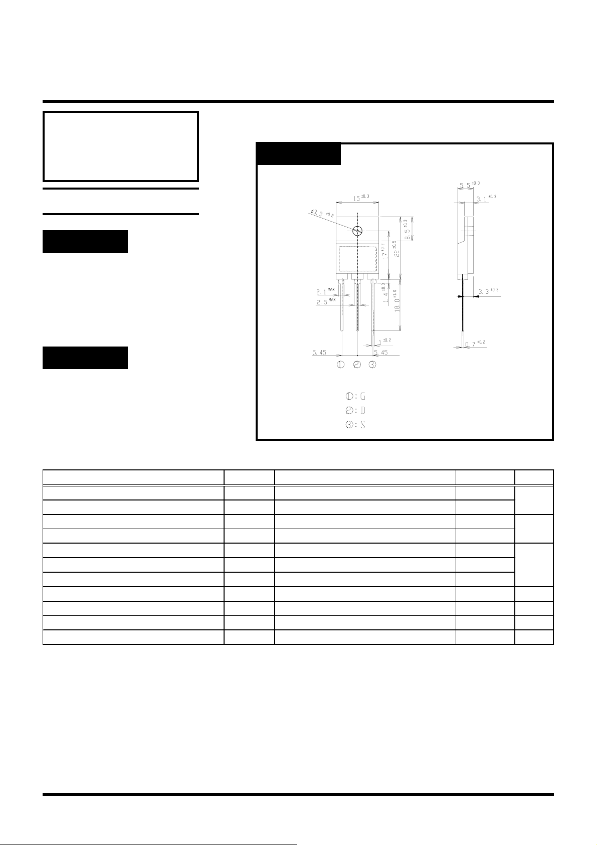
OUTLINE DIMENSIONS
Case : E-pack
Case : ITO-3P
(Unit : mm)
RATINGS
●Absolute Maximum Ratings (Tc = 25℃)
Item Symbol Conditions Ratings Unit
Storage Temperature
Channel Temperature
Drain-Source Voltage
Gate-Source Voltage
Continuous Drain Current(DC)
Continuous Drain Current(Peak)
Continuous Source Current(DC)
Total Power Dissipation
Single Pulse Avalanche Current
Dielectric Strength
Mounting Torque
T
T
V
DSS
V
GSS
I
I
DP
I
P
I
AS
V
TOR
stg
ch
D
S
T
ch
T
= 25℃
dis
Terminals to case, AC 1 minute
( Recommended torque : 0.5N・m )
-55~150 ℃
150
500 V
±30
15
45 A
15
60 W
15A
2kV
0.8 N・m
Copyright & Copy;2000 Shindengen Electric Mfg.Co.Ltd
Page 2

VX-2 Series Power MOSFET
●Electrical Characteristics Tc = 25℃
Item Symbol Conditions Min. Typ. Max. Unit
Drain-Source Breakdown Voltage
Zero Gate Voltage Drain Current
Gate-Source Leakage Current
Forward Transconductance
Static Drain-Source On-state Resistance
Gate Threshold Voltage
Source-Drain Diode Forwade Voltage
Thermal Resistance
Total Gate Charge
Input Capacitance
Reverse Transfer Capacitance
Output Capacitance
Turn-On Time
Turn-Off Time
V
(BR)DSSID
I
DSS
I
GSS
g
fs
R
DS(ON)ID
V
THID
V
SDIS
θjc
Q
g
C
iss
C
rss
C
oss
t
on
t
off
2SK2195 ( FP15W50VX2 )
= 1mA, VGS = 0V
VDS = 500V, VGS = 0V
VGS = ±30V, VDS = 0V
ID = 7.5A, VDS = 10V
= 7.5A, VGS = 10V
= 1mA, VDS = 10V
= 7.5A, VGS = 0V
junction to case
VDD = 400V, VGS = 10V, ID = 15A
VDS = 10V, VGS = 0V, f = 1MH
ID = 7.5A, VGS = 10V, RL = 20Ω
Z
500 V
250 μA
±0.1
4.5 10S
0.35 0.45 Ω
2.5 3.0 3.5 V
1.5
2.08 ℃/W
65 nC
1900
135 pF
400
110 180 ns
270 440
Copyright & Copy;2000 Shindengen Electric Mfg.Co.Ltd
Page 3

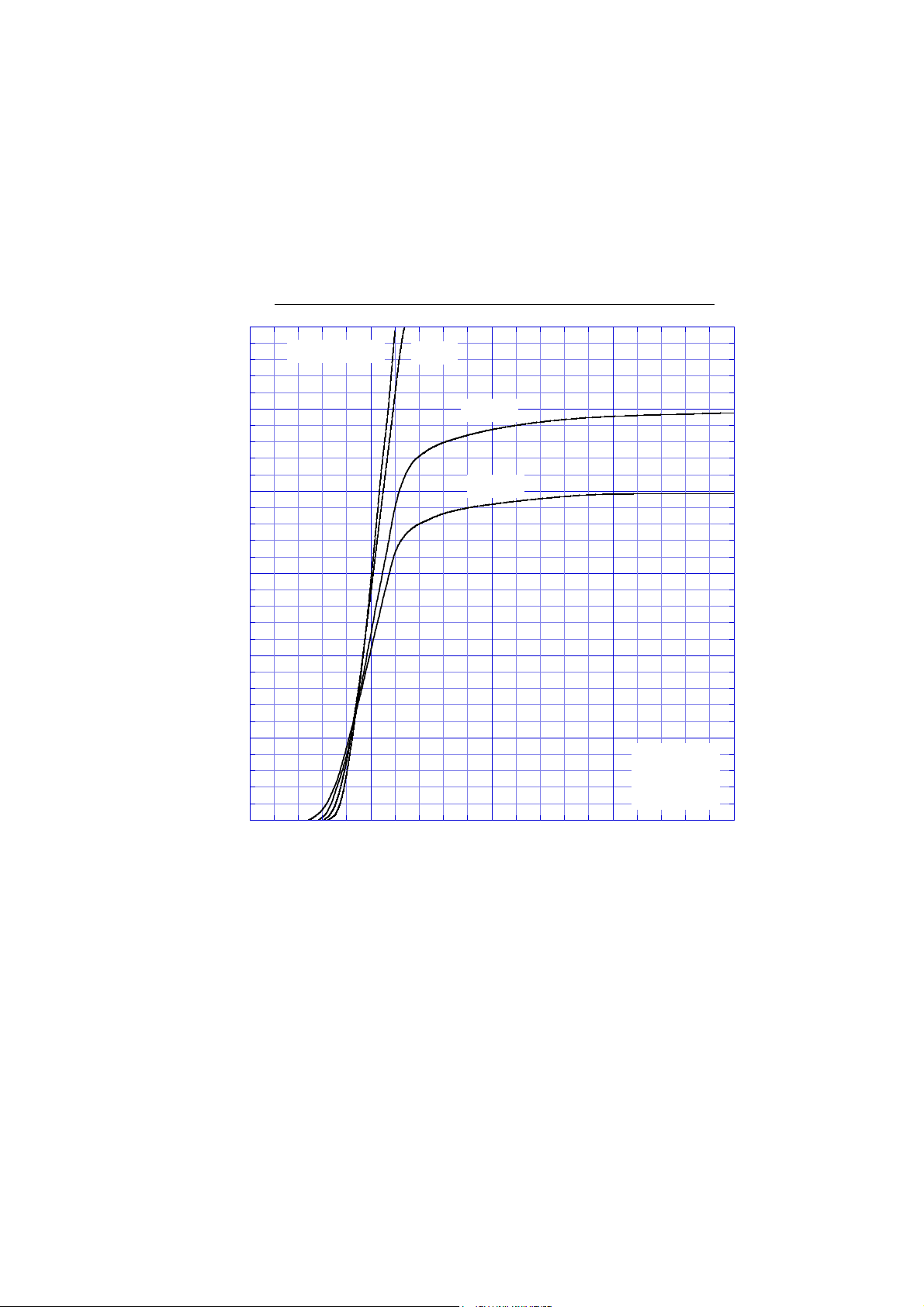
30
2SK2195 Transfer Characteristics
Tc = −55°C
25°C
25
20
[A]
D
15
10
100°C
150°C
Drain Current I
5
VDS = 25V
pulse test
TYP
0
0 5 10 15 20
Gate-Source Voltage VGS [V]
Page 4

2SK2195
[Ω]
1
DS(ON)
Static Drain-Source On-state Resistance
ID = 7.5A
0.1
Static Drain-Source On-state Resistance R
-50 0 50 100 150
Case Temperature Tc [°C]
VGS = 10V
pulse test
TYP
Page 5

[V]
TH
2SK2195
5
4
3
2
Gate Threshold Voltage
Gate Threshold Voltage V
1
0
-50 0 50 100 150
Case Temperature Tc [°C]
VDS = 10V
ID = 1mA
TYP
Page 6

100
2SK2195
Safe Operating Area
10
R
[A]
D
1
DS(ON)
limit
Drain Current I
0.1
Tc = 25°C
Single Pulse
100µs
200µs
1ms
10ms
DC
0.01
1 10 100 1000
Drain-Source Voltage VDS [V]
Page 7

2
10
1
10
0
10
-1
10
Transient Thermal Impedance
2SK2195
100
10
-2
Time t [s]
10
-3
10
-4
10
-5
1
0.1
10
0.01
Transient Thermal Impedance θjc(t) [°C/W]
Page 8

10000
0.005
Tc=25°C
TYP
Ciss
Coss
Crss
Drain-Source Voltage VDS [V]
1000
2SK2195
Capacitance
100
Capacitance Ciss Coss Crss [pF]
10
0 20 40 60 80 100
Page 9

2SK2195 Power Derating
100
80
60
40
Power Derating [%]
20
0
0 50 100 150
Case Temperature Tc [°C]
Page 10

2SK2195
Gate Charge Characteristics
500
400
[V]
DS
300
200
Drain-Source Voltage V
100
V
DS
VDD = 400V
200V
100V
V
20
15
[V]
GS
10
GS
5
Gate-Source Voltage V
ID = 15A
0
0 20 40 60 80 100
Gate Charge Qg [nC]
0
 Loading...