


Datadelay PPG33F-0.5, PPG33F-0.5C3, PPG33F-0.5M, PPG33F-0.5MC3, PPG33F-1 Datasheet
...
PPG33F
Doc #97010 DATA DELAY DEVICES, INC. 1
1/15/97 3 Mt. Prospect Ave. Clifton, NJ 07013
3-BIT PROGRAMMABLE
PULSE GENERATOR
(SERIES PPG33F)
FEATURES PACKAGES
• Digitally programmable in 7 steps
• Monotonic pulse-width-vs-address variation
• Rising edge triggered
• Two separate outputs: inverting & non-inverting
• Precise and stable pulse width
• Input & outputs fully TTL interfaced & buffered
• 10 T2L fan-out capability
• Fits standard 14-pin DIP socket
• Auto-insertable
FUNCTIONAL DESCRIPTION
The PPG33F-series device is a 3-bit digitally programmable pulse
generator. The width, PWA, depends on the address code (A2-A0)
according to the following formula:
PWA = PW0 + T
INC
* A
where A is the address code, T
INC
is the incremental pulse width of the
device, and PW0 is the inherent pulse width of the device. The
incremental width is specified by the dash number of the device and can range from 0.5ns through 50ns,
inclusively. RESET is held LOW during normal operation. When it is brought HIGH, OUT and OUT/ are
forced into LOW and HIGH states, respectively, and the unit is ready for the next trigger input. The
address is not latched and must remain asserted while the output pulse is active.
SERIES SPECIFICATIONS
• Programmed pulse width tolerance: 5% or 1ns,
whichever is greater
• Inherent width (PW0):9ns typical
• Inherent delay (TTO): 3.5ns ± 2ns
• Operating temperature: 0° to 70° C
• Supply voltage VCC: 5VDC ± 5%
• Supply current: ICC = 41ma typical
1997 Data Delay Devices
data
delay
devices, inc.
3
16
15
14
13
12
11
10
9
1
2
3
4
5
6
7
8
TRIG
OUT
N/C
N/C
N/C
N/C
RES
GND
VCC
OUT/
N/C
N/C
N/C
A0
A1
A2
14
13
12
11
10
9
8
1
2
3
4
5
6
7
TRIG
OUT
N/C
N/C
N/C
RES
GND
VCC
OUT/
N/C
N/C
A0
A1
A2
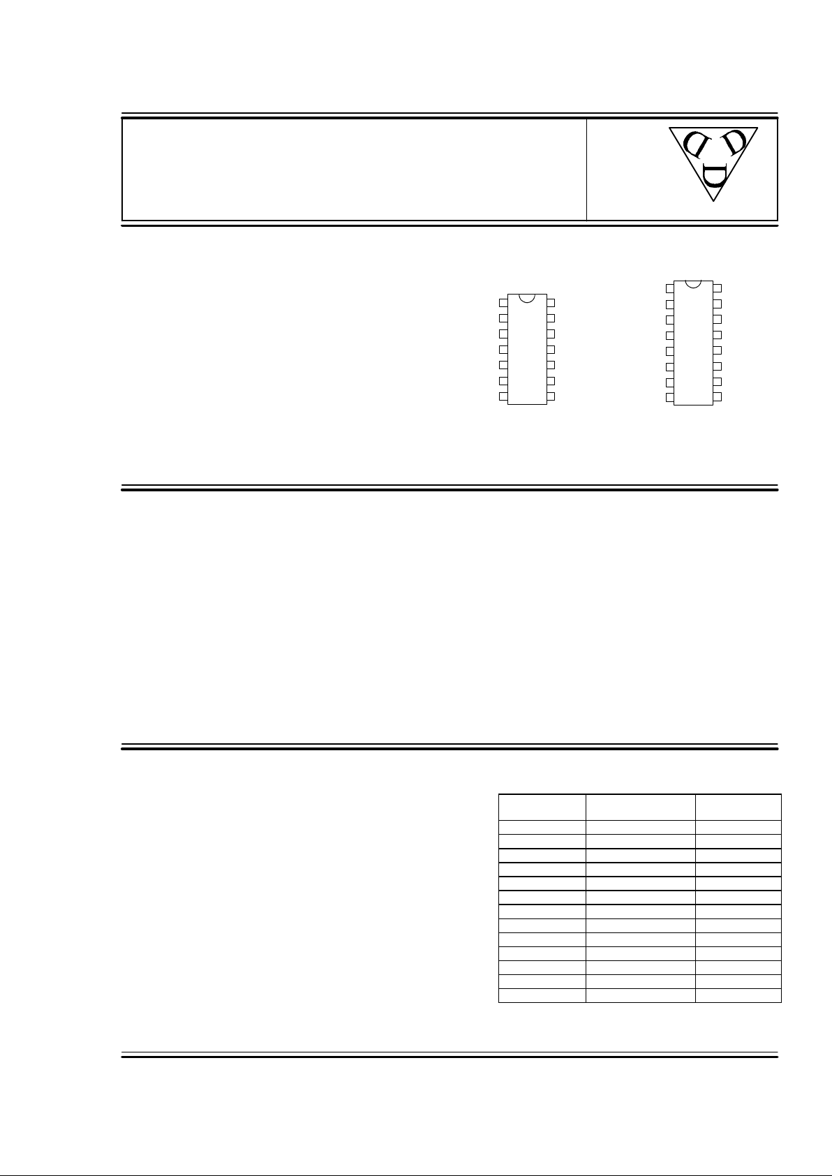
DIP
PPG33F-xx Commercial
PPG33F-xxM Military
Gull-Wing
PPG33F-xxC3 Commercial
PPG33F-xxMC3 Military
PIN DESCRIPTIONS
TRIG Trigger Input
OUT Non-inverted Output
OUT/ Inverted Output
A0-A2 Address Bits
RES Reset
VCC +5 Volts
GND Ground
DASH NUMBER SPECIFICATIONS
Part
Number
Incremental Width
Per Step (ns)
Total Width
Change (ns)
PPG33F-.5
0.5 ± 0.3 3.50 ± 1.00
PPG33F-1
1 ± 0.4 7.00 ± 1.00
PPG33F-2
2 ± 0.4 14.0 ± 1.00
PPG33F-3
3 ± 0.5 21.0 ± 1.05
PPG33F-4
4 ± 0.5 28.0 ± 1.40
PPG33F-5
5 ± 0.6 35.0 ± 1.75
PPG33F-6
6 ± 0.7 42.0 ± 2.10
PPG33F-8
8 ± 0.8 56.0 ± 2.80
PPG33F-10
10 ± 1.0 70.0 ± 3.50
PPG33F-20
20 ± 1.5 140 ± 7.00
PPG33F-30
30 ± 1.8 210 ± 10.5
PPG33F-40
40 ± 2.0 280 ± 14.0
PPG33F-50
50 ± 2.5 350 ± 17.5
NOTE: Any dash number between .5 and 50 not
shown is also available.

PPG33F
Doc #97010 DATA DELAY DEVICES, INC. 2
1/15/97 Tel: 973-773-2299 Fax: 973-773-9672 http://www.datadelay.com
APPLICATION NOTES
DEVICE TIMING
The timing definitions and restrictions for the
PPG33F are shown in Figure 1. The unit is
activated by a rising edge on the TRIG input.
After a time, TTO (called the inherent delay), the
rising edge of the pulse appears at OUT. The
duration of the pulse is given by the above
equation. For the duration of the pulse, the
device ignores subsequent triggers. Once the
falling edge of the pulse has appeared at OUT,
an additional time, T
OTR
, is required before the
device can respond to the next trigger.
At power-up, the state of the PPG33F is
unknown. Consequently, after power is applied,
the unit may not respond to input triggers for a
time equal to the maximum pulse width, PWT.
After this time, the unit will function properly. If
your application requires that the device function
immediately, issue a quick reset at power-up.
POWER SUPPLY BYPASSING
The PPG33F relies on a stable power supply to
produce repeatable pulses within the stated
tolerances. A 0.1uf capacitor from VCC to GND,
located as close as possible to each VCC pin, is
recommended. A wide VCC trace should
connect all VCC pins externally, and a clean
ground plane should be used.
INCREMENT TOLERANCES
Please note that the increment tolerances listed
represent a design goal. Although most
increments will fall within tolerance, they are not
guaranteed throughout the address range of the
unit. Monotonicity is, however, guaranteed over
all addresses.
`
T
OAX
T
RTS
T
TW
T
TO
PW
A
A2-A0
RES
TRIG
OUT
OUT/
Figure 1: Timing Diagram
A
i
A
i+1
T
SKEW
T
ATS
T
RO
T
OTR
T
TW
T
RW
 Loading...