


PDU1064H-1C5
Datadelay PDU1064H-1C5, PDU1064H-1M, PDU1064H-1MC5, PDU1064H-2, PDU1064H-2C5 Datasheet
...
PDU1064H
Doc #97046 DATA DELAY DEVICES, INC. 1
12/17/97 3 Mt. Prospect Ave. Clifton, NJ 07013
6-BIT, ECL-INTERFACED
PROGRAMMABLE DELAY LINE
(SERIES PDU1064H)
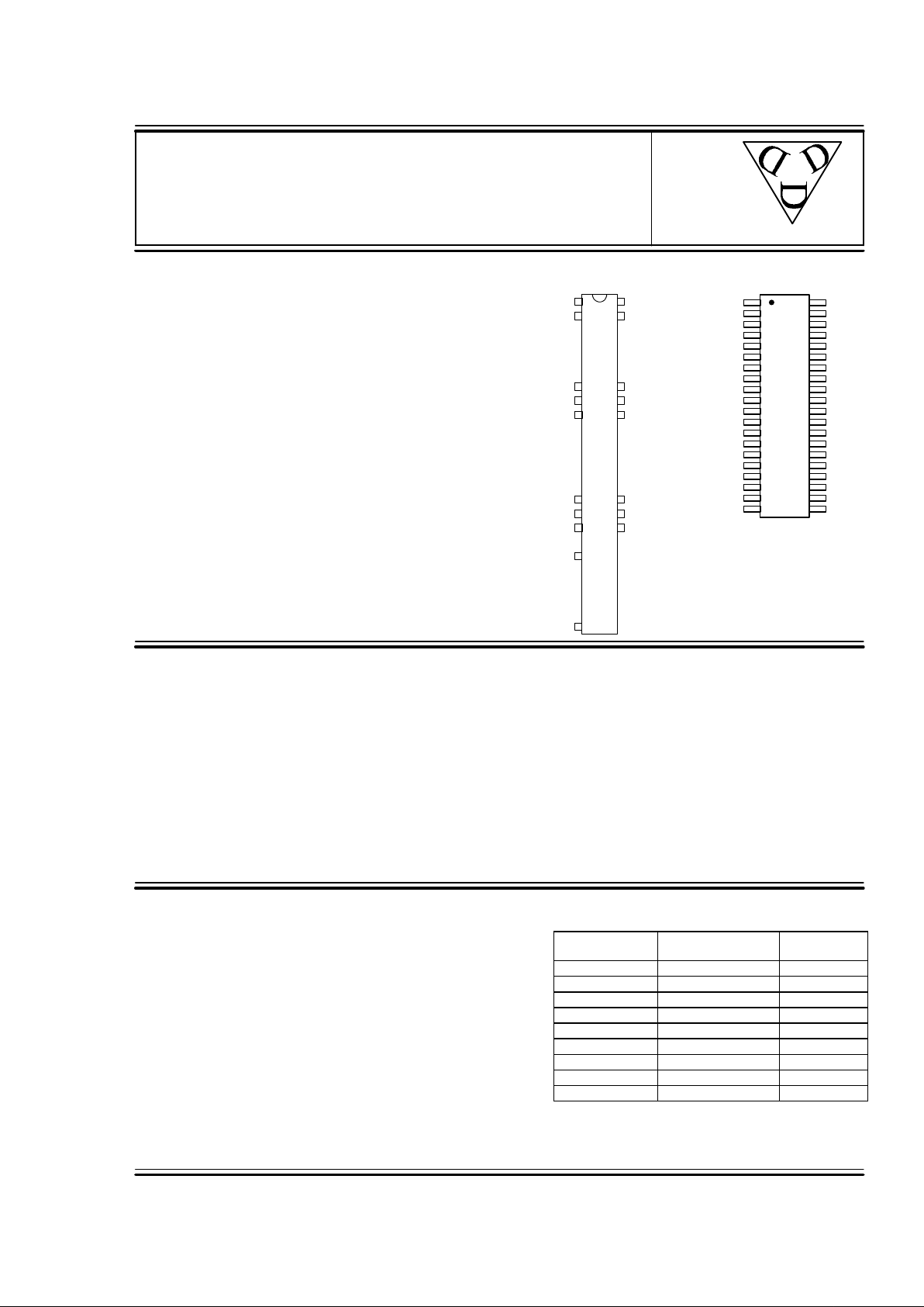
FEATURES PACKAGES
• Digitally programmable in 64 delay steps
• Monotonic delay-versus-address variation
• Precise and stable delays
• Input & outputs fully 10KH-ECL interfaced & buffered
• Fits 48-pin DIP socket
PIN DESCRIPTIONS
IN Signal Input
OUT Signal Output
A0-A5 Address Bits
ENB Output Enable
VEE -5 Volts
GND Ground
FUNCTIONAL DESCRIPTION
The PDU1064H-series device is a 6-bit digitally programmable delay line. The delay, TDA, from the input
pin (IN) to the output pin (OUT) depends on the address code (A5-A0) according to the following formula:
TDA = TD0 + T
INC
* A
where A is the address code, T
INC
is the incremental delay of the device, and TD0 is the inherent delay of
the device. The incremental delay is specified by the dash number of the device and can range from
0.5ns through 10ns, inclusively. The enable pin (ENB) is held LOW during normal operation. When this
signal is brought HIGH, OUT is forced into a LOW state. The address is not latched and must remain
asserted during normal operation.
SERIES SPECIFICATIONS
• Total programmed delay tolerance: 5% or 2ns,
whichever is greater
Inherent delay (TD0): 12ns typical
• Setup time and propagation delay:
Address to input setup (T
AIS
): 3.6ns
Disable to output delay (T
DISO
): 1.7ns typical
• Operating temperature: 0° to 70° C
• Temperature coefficient: 100PPM/°C (excludes TD0)
• Supply voltage VEE: -5VDC ± 5%
• Power Dissipation: 925mw typical (no load)
• Minimum pulse width: 20% of total delay
1997 Data Delay Devices
data
delay
devices, inc.
3
1
2
3
4
5
6
7
8
9
10
11
12
13
14
15
16
17
18
19
20
40
39
38
37
36
35
34
33
32
31
30
29
28
27
26
25
24
23
22
21
N/C
N/C
OUT
GND
ENB
N/C
N/C
N/C
GND
ENB
N/C
N/C
N/C
N/C
N/C
N/C
N/C
GND
ENB
IN
N/C
N/C
A2
A1
VEE
A0
N/C
A5
A4
VEE
A3
N/C
N/C
N/C
N/C
N/C
N/C
N/C
VEE
N/C
GND
IN
VEE
GND
ENB
A0
VEE
48
47
42
41
1
2
7
8
GND
OUT
A1
A2
GND
A3
VEE
40
34
33
9
15
16
GND
A4
A5
3217
19
24
GND
PDU1064H-xxC5 SMD
PDU1064H-xxMC5 Mil SMD
PDU1064H-xx DIP
PDU1064H-xxM Mil DIP
DASH NUMBER SPECIFICATIONS
Part
Number
Incremental Delay
Per Step (ns)
Total
Delay (ns)
PDU1064H-.5
0.5 ± 0.3 31.5 ± 2.0
PDU1064H-1
1.0 ± 0.5 63 ± 3.1
PDU1064H-2
2.0 ± 0.5 126 ± 6.3
PDU1064H-3
3.0 ± 1.0 189 ± 9.4
PDU1064H-4
4.0 ± 1.0 252 ± 12.6
PDU1064H-5
5.0 ± 1.0 315 ± 15.7
PDU1064H-6
6.0 ± 1.0 378 ± 18.9
PDU1064H-8
8.0 ± 1.0 504 ± 25.2
PDU1064H-10
10.0 ± 1.5 630 ± 31.5
NOTE: Any dash number between .5 and 10
not shown is also available.
PDU1064H
Doc #97046 DATA DELAY DEVICES, INC. 2
12/17/97 Tel: 973-773-2299 Fax: 973-773-9672 http://www.datadelay.com
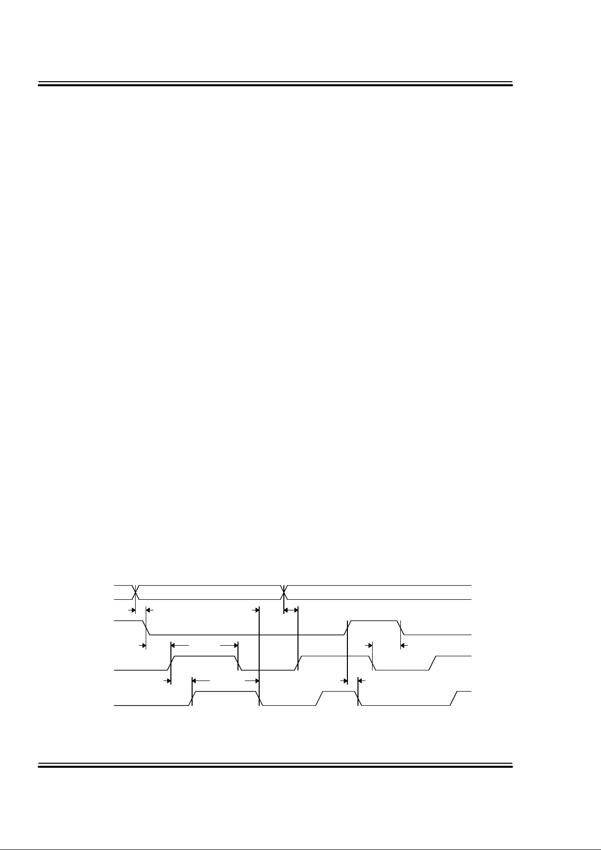
APPLICATION NOTES
ADDRESS UPDATE
The PDU1064H is a memory device. As such,
special precautions must be taken when
changing the delay address in order to prevent
spurious output signals. The timing restrictions
are shown in Figure 1.
After the last signal edge to be delayed has
appeared on the OUT pin, a minimum time,
T
OAX
, is required before the address lines can
change. This time is given by the following
relation:
T
OAX
= max { (Ai - A
i-1
) * T
INC
, 0 }
where A
i-1
and Ai are the old and new address
codes, respectively. Violation of this constraint
may, depending on the history of the input signal,
cause spurious signals to appear on the OUT
pin. The possibility of spurious signals persists
until the required T
OAX
has elapsed.
A similar situation occurs when using the ENB
signal to disable the output while IN is active. In
this case, the unit must be held in the disabled
state until the device is able to “clear” itself. This
is achieved by holding the ENB signal high and
the IN signal low for a time given by:
T
DISH
= Ai * T
INC
Violation of this constraint may, depending on
the history of the input signal, cause spurious
signals to appear on the OUT pin. The
possibility of spurious signals persists until the
required T
DISH
has elapsed.
INPUT RESTRICTIONS
There are three types of restrictions on input
pulse width and period listed in the AC
Characteristics table. The recommended
conditions are those for which the delay
tolerance specifications and monotonicity are
guaranteed. The suggested conditions are
those for which signals will propagate through the
unit without significant distortion. The absolute
conditions are those for which the unit will
produce some type of output for a given input.
When operating the unit between the
recommended and absolute conditions, the
delays may deviate from their values at low
frequency. However, these deviations will
remain constant from pulse to pulse if the input
pulse width and period remain fixed. In other
words, the delay of the unit exhibits frequency
and pulse width dependence when operated
beyond the recommended conditions. Please
consult the technical staff at Data Delay Devices
if your application has specific high-frequency
requirements.
Please note that the increment tolerances listed
represent a design goal. Although most delay
increments will fall within tolerance, they are not
guaranteed throughout the address range of the
unit. Monotonicity is, however, guaranteed over
all addresses.
T
DISO
T
OAX
T
AENS
T
ENIS
PW
IN
TD
A
PW
OUT
T
DISH
A5-A0
ENB
IN
OUT
Figure 1: Timing Diagram
A
i-1
A
i
T
AIS
 Loading...