

DAEWOO DV-F24J Service Manual

SYSTEM
Video signal NTSC color
Channel coverage VHF Channel 1-12
UHF Channel 13-62
CATV Channel C13-C35
VHF output signal Channel 1 or 2 (selectable)
VIDEO
Input: Video line in Phono-type connector
1.0V (p-p)
75 ohms unbalanced, sync.
negative
Output: Video line out Phono-type connector
1.0V (p-p)
75 ohms unbalanced, sync.
negative
Signal to noise ratio More than 43dB (SP)
Horizontal resolution 230 lines
AUDIO
Input: Audio Line in Phono-type connector
more than 47K ohms,
–8 dBm, unbalanced
Output: Audio line out Phono-type connector
less than 1K ohms,
–6dBm (more than 47K ohms
load), unbalanced
Frequency response 100 Hz-10KHz (SP)
Signal to noise ratio More than 40 dB
Audio Distortion Less than 3% (SP)
TAPE TRANSPOR T
Tape width 12.65mm (1/2")
Tape speed SP: 33.35 mm/sec
LP: 16.67 mm/sec
EP: 11.12 mm/sec
Maximum recording time 480 min, with T-160 tape (EP)
FF. REW time Approx 5 min (T-120)
GENERAL
Power requirements 100V, 50Hz AC only
Power consumption 17W
DIMENSIONS
Set size (WxHxD) 360x90x312 mm
Carton size (WxHxD) 431x175x397 mm
Weight (gross) 5.4Kg (11.9 lbs)
SPECIFICATIONS
• Safety Check after Servicing
Examine the area surrounding the repaired location for damage or deterioration. Observe that screws, parts and wires
have been returned to original positions. Afterwards, perform the following tests and confirm the specified values in order
to verify compliance with safety standards.
1. Insulation resistance test
Confirm the specified insulation resistance or greater between power cord plug prongs and externally exposed parts of
the set (RF terminals, antenna terminals, video and audio input and output terminals, microphone jacks, earphone
jacks, etc.). See table below.
2. Dielectric strength test
Confirm specified dielectric strength or greater between power cord plug prongs and exposed accessible parts of the
set (RF terminals, antenna terminals, video and audio input and output terminals, microphone jacks, earphone jacks,
etc.) See table below.
3. Clearance distance
When replacing primary circuit components, confirm
specified clearance distance (d), (d') between soldered
terminals, and between terminals and surrounding
metalic parts. See table below.
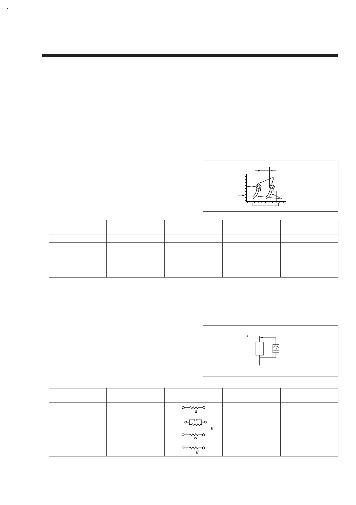
Table 1: Rating for selected areas
* Class II model only.
Note: This table is unofficial and for reference only. Be sure to confirm the precise values for your particular country and
locality.
4. Leakage current test
Confirm specified or lower leakage current between B (earth ground, power cord plug prongs) and externally exposed
accessible parts (RF terminals, antenna terminals, video and audio input and output terminals, microphone jacks,
earphone jacks, etc.)
Measuring Method: (Power ON)
Insert load Z between B (earth ground, power cord plug
prongs) and exposed accesible parts. Use and AC
voltmeter to measure across both terminals of load Z.
See figure and following table.
Table 2: Leakage current ratings for selected areas
Note: This table unofficial and for reference only. Be sure to confirm the precise values for your particular country and
locality.
Fig. 2
AC Line Voltage Region
Insulation Dielectric Clearance
Resistance Strength Distance (d), (d')
100V Japan ≥ 1 MΩ/500 VDC 1kV 1 minute ≥ 3 mm
110 to 130V
USA &
– – –
900V 1 minute ≥ 3.2mm
Canada
* 110 to 130 V Europe ≥ 10 MΩ/500 VDC 4 kV 1 minute ≥6 mm (d)
200 to 240 V Australia ≥ 8 mm (d')
(a: Power cord)
AC Line Voltage Region
Earth Ground
Load Z Leakage Current (i)
(B) to:
100V Japan ¡ ≤ 1m A rms
Exposed accessible
parts
110 to 130 V USA & ¡ ≤ 0.5 m A rms Exposed accessible
parts
¡ ≤ 0.7 m A peak Antenna earth
110 to 130 V Europe ¡ ≤ 2 m A dc terminals
200 to 240 V Australia ¡ ≤ 0.7 m A peak
Other terminals
¡ ≤ 2 m A dc
Fig. 1
1k
1.5k
1.5kµF
2k
50k
d
Primary circuit termimals
Chassis
d'
a
Exposed
accessible
part
Z
Earth Ground
power cord plug prongsB
AC Voltmeter
(high impedance)

TABLE OF CONTENTS
SECTION 1. CONTROLS AND FUNCTIONS..........................................................................................................2
SECTION 2. ELECTRICAL ADJUSTMENTS
2-1. SERVO CIRCUIT ADJUSTMENT METHOD.....................................................................................................................3
2-2. VIDEO CIRCUIT ADJUSTMENT METHOD.......................................................................................................................4
2-3. AUDIO CIRCUIT ADJUSTMENT METHOD.................................................................................................................... 10
SECTION 3. TROUBLE SHOOTING FLOW CHART
3-1. POWER CIRCUIT.............................................................................................................................................................11
3-2. LOGIC CIRCUIT...............................................................................................................................................................13
3-3. SERVO/SYSCON CIRCUIT.............................................................................................................................................16
3-4. AUDIO CIRCUIRT............................................................................................................................................................21
3-5. VIDEO CIRCUIT ...............................................................................................................................................................23
SECTION 4. BLOCK DIAGRAM
4-1. Y.C./HEAD AMP/AUDIO/INPUT SELECTOR BLOCK DIAGRAM.......................................................................... .......27
4-2. SYSCON/LOGIC BLOCK DIAGRAM................................................................................................ .............................. 28
4-3. PIF/OSD BLOCK DIAGRAM ...........................................................................................................................................29
SECTION 5. CIRCUIT DIAGRAM
5-1. CONNECTION DIAGRAM...............................................................................................................................................30
5-2. POWER CIRCUIT (SMPS)...............................................................................................................................................31
5-3. SYSCON CIRCUIT............................................................................................................ ............................................... 33
5-4. TIMER CIRCUIT...............................................................................................................................................................34
5-5. PIF & INPUT SELECTOR CIRCUIT.................................................................................................................................35
5-6. HEAD-AMP CIRCUIT.......................................................................................................................................................36
5-7. VIDEO CIRCUIT ...............................................................................................................................................................37
5-8. AUDIO CIRCUIT............................................................................................................................................................... 38
5-9. OSD CIRCUIT...................................................................................................................................................................39
5-10. REMOCON CIRCUIT.....................................................................................................................................................40
SECTION 6. VOLT AGE CHAR T
6-1. IC VOLTAGE.....................................................................................................................................................................41
6-2. TR VOLTAGE....................................................................................................................................................................48
SECTION 7. COMPONENTS LOCA TION GUIDE ON PCB (BOTTOM VIEW)
7-1. PCB HEAD-AMP..............................................................................................................................................................49
7-2. PCB MAIN........................................................................................................................................................................50
7-3. PCB LOGIC......................................................................................................................................................................51
SECTION 8. DISASSEMBLY
8-1. PACKING AS....................................................................................................................................................................52
8-2. SET TOTAL ASSEMBLY..................................................................................................................................................53
SECTION 9. ELECTRICAL P AR TS LIST
9-1. STANDARD PART NUMBER CODING ..........................................................................................................................54
9-2. ELECTRICAL PARTS LIST..............................................................................................................................................56
APPENDIX
VCR MECHANISM TECHNICAL SERVICE GUIDE...........................................................................................65
1
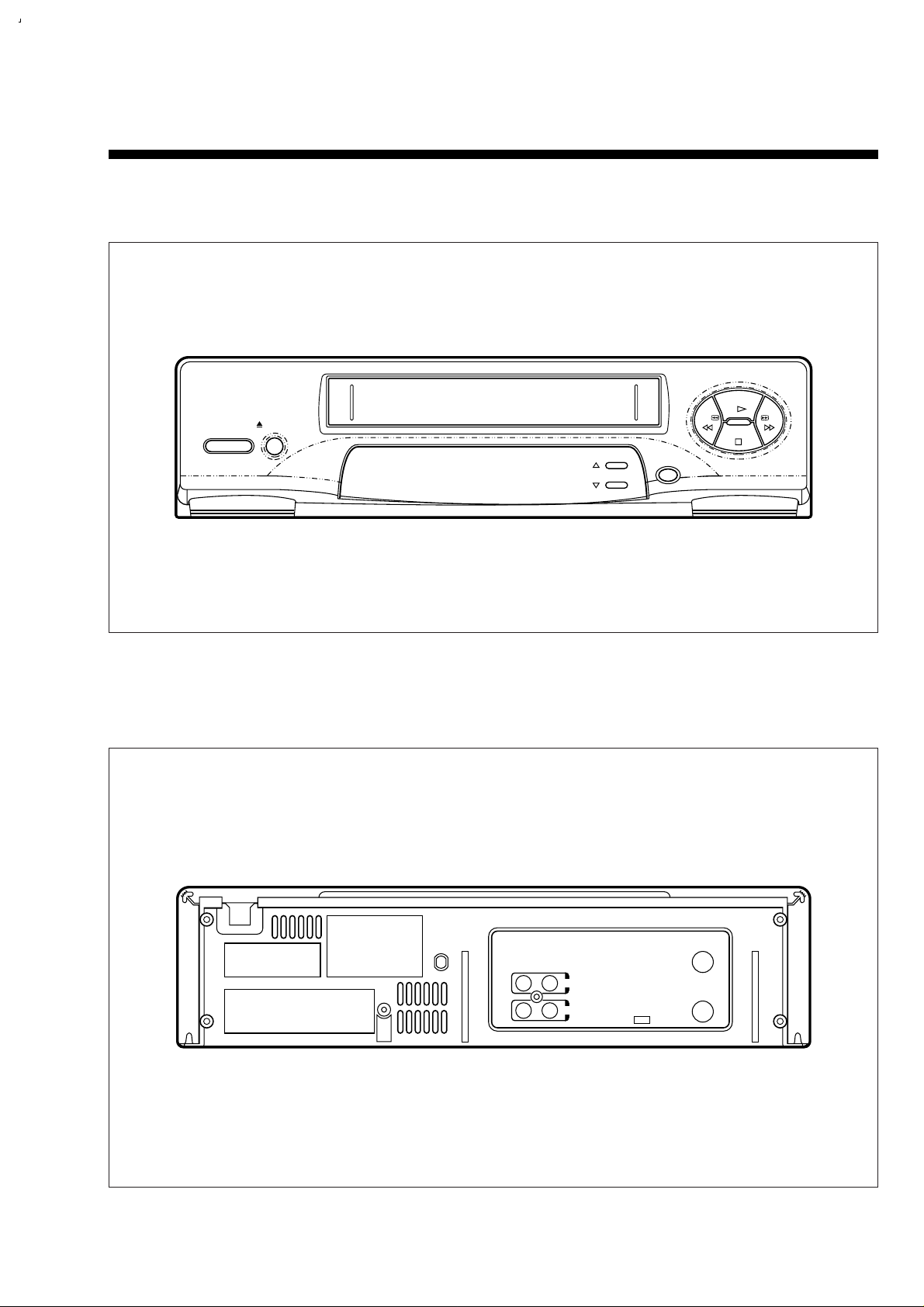
SECTION 1. CONTROLS AND
2
POWER
EJECT
REC /OTR
CH/TRACK
REW FF
PLAY
STOP
FRONT
DV-F24J
VIDEO AUDIO
CH.1 CH.2
RF OUT
ANT.IN
IN
OUT
REAR
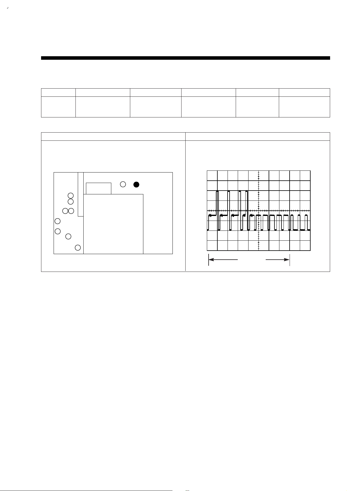
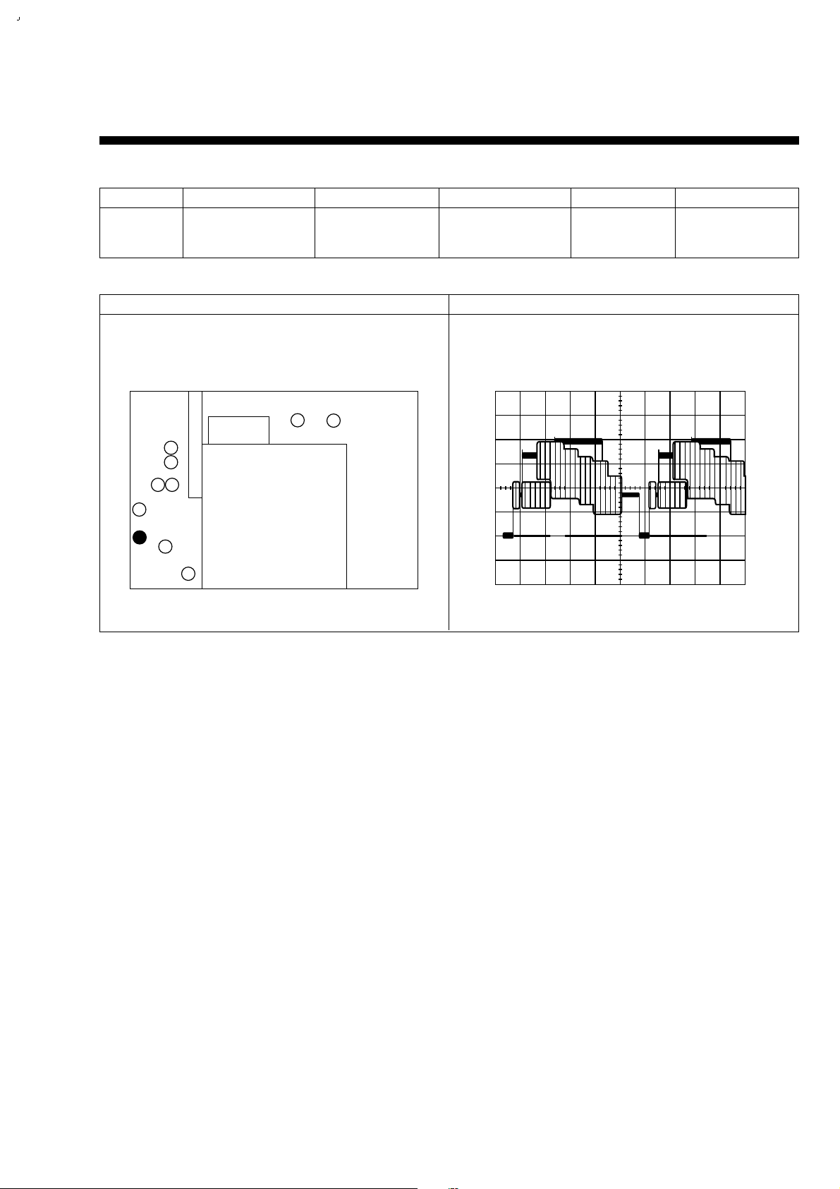
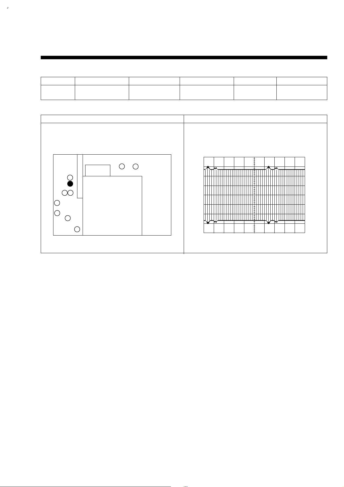
2-1. SERVO CIRCUIT ADJUSTMENT METHOD
1. PB Phase
• Adjustment Procedure
1. Set the oscilloscope to the CHOP mode. Connect the oscilloscope to check point and trigger the scope with CH1.
2. Adjust R595 to position the V-SYNC at 6.5±0.5H from the rising edge of sw pulse.
• Adjustment Inspection Standard: 6.5±0.5 H
SECTION 2. ELECTRICAL ADJUSTMENT
Mode Adjustment Parts Check Point Test Equipments Test Tape Input Signal
CH 1: PT01 #
PB ! R595 CH 2: VIDEO Oscilloscope DN-1
OUTPUT JACK
3
Location of Adjustment Parts Observation Waveform
H-Axis: 50us/div V-Axis: CH 1 ¡ 1.0v/div
CH2 ¡ 0.5v/div
MAIN PCB
T
U
N
E
R
HEAD-AMP
DECK
8
9
63
7
4
5
2
10
1
6.5¡ 0.5H
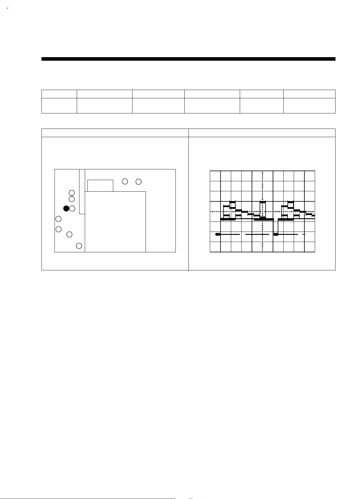
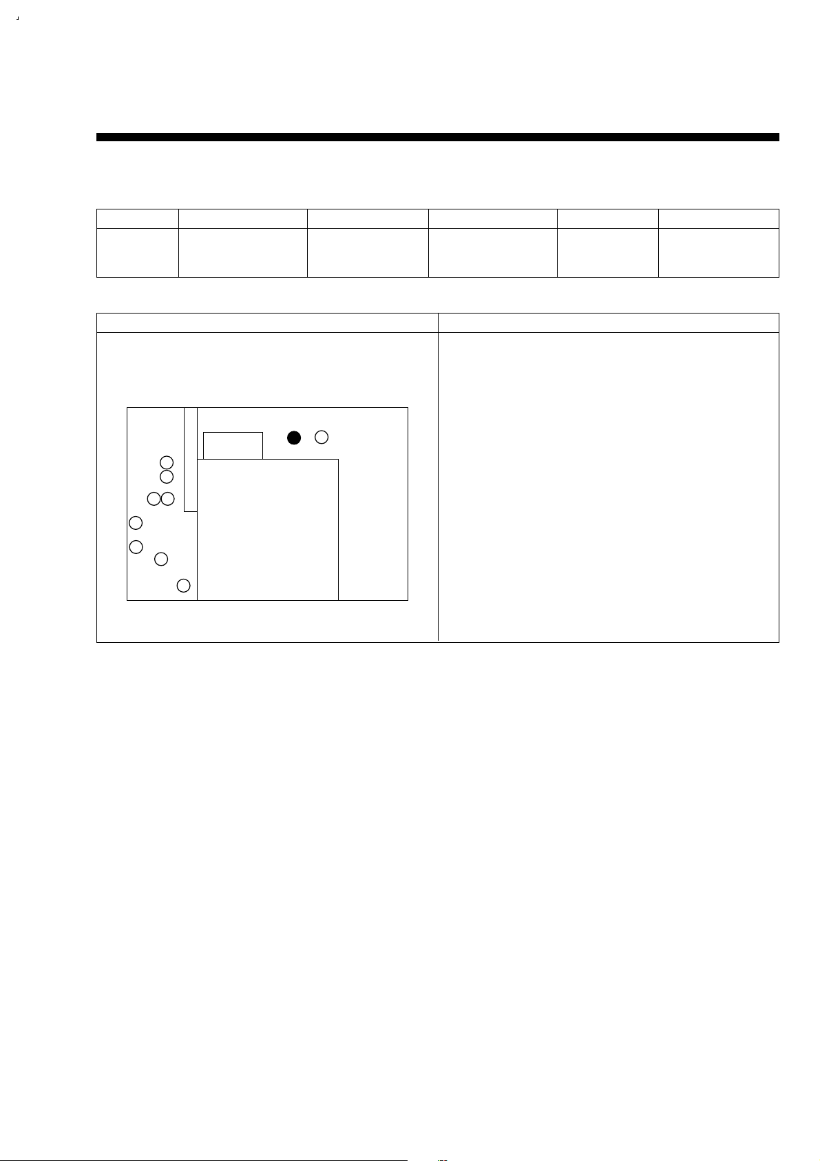
2-2. VIDEO CIRCUIT ADJUSTMENT METHOD
1. EE LEVEL
• Adjustment Procedure
1. Set the TV/LINE to LINE mode.
2. Supply the color bar signal with 100% white to video input jack.
3. Set the VCR to the stop mode.
4. Connect the oscilloscope to check point and trigger the scope with CH2.
5. Adjust R395 to obtain 0.5±0.01 Vp-p between the sync tip and 100% white level.
• Adjustment Inspection Standard: 0.5±0.01 Vp-p
4
Mode Adjustment Parts Check Point Test Equipments Test Tape Input Signal
LINE INPUT CH1: TJ313 Signal Gen. Color Bar
& STOP
# R395
CH2: TJ395 Oscilloscope with 100% white
Location of Adjustment Parts Observation Waveform
H-Axis: 10us/div V-Axis: 0.1v/div
MAIN PCB
T
U
HEAD-AMP
N
8
E
9
R
63
7
4
5
2
DECK
10
1
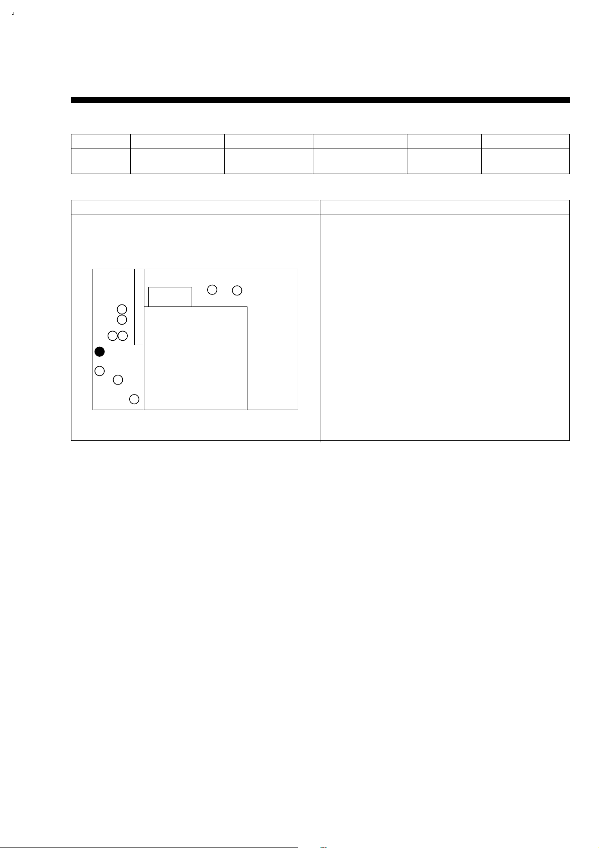
2. PLAYBACK VIDEO OUTPUT LEVEL
• Adjustment Procedure
1. Playback the color bar test tape (DN-1).
2. Connect the oscilloscope to check point and trigger the scope with CH1.
3. Adjust R396 to obtain 2.0±0.2 Vp-p between the sync tip and 100% white level.
• Adjustment Inspection Standard: 2.0±0.2 Vp-p
5
Mode Adjustment Parts Check Point Test Equipments Test Tape Input Signal
CH 1: TJ313
PB $ 396 CH 2: VIDEO Oscilloscope DN-1
OUTPUT JACK
Location of Adjustment Parts Observation Waveform
H-Axis: 50us/div V-Axis: 0.5v/div
MAIN PCB
T
U
HEAD-AMP
N
8
E
9
R
63
7
4
5
2
DECK
10
1
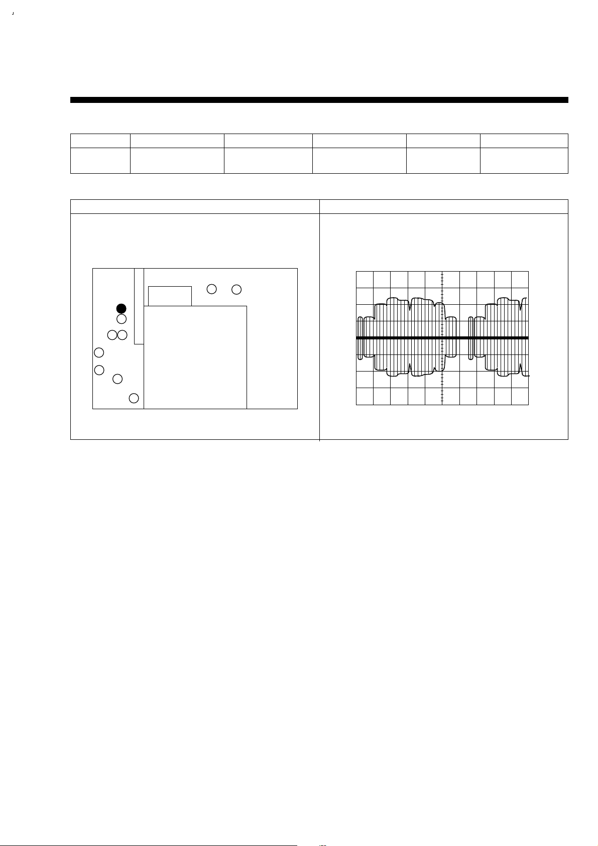
3. COMB PHASE
• Adjustment Procedure
1. Set the TV/LINE to LINE mode.
2. Supply the multiburst signal to video input jack.
3. Set the VCR to the stop mode.
4. Connect the oscilloscope to check point and trigger the scope with CH1.
5. Adjust R494 until the 3.58 MHz component of multiburst signal becomes minimum.
• Adjustment Inspection Standard: Minimum
6
Mode Adjustment Parts Check Point Test Equipments Test Tape Input Signal
LINE INPUT CH1: TJ313 Signal Gen.
& STOP
% R494
CH2: TJ494 Oscilloscope
Multiburst
Location of Adjustment Parts Observation Waveform
H-Axis: 10us/div V-Axis: 20mv/div
MAIN PCB
T
U
HEAD-AMP
N
8
E
9
R
63
7
4
5
2
DECK
10
1
3. SYNC TIP FREQ.
• Adjustment Procedure
1. Set the TV/LINE to LINE mode.
2. Set the VCR to the STOP mode.
3. Connect the frequency counter to check point.
4. Adjust R391 to obtain 3.33±0.1 MHz.
• Adjustment Inspection Standard: 3.33±0.1 MHz
7
Mode Adjustment Parts Check Point Test Equipments Test Tape Input Signal
+: TJ391
STOP & R391
–: GND
Freq. Counter Without signal
Location of Adjustment Parts Observation Waveform
H-Axis: V-Axis:
MAIN PCB
T
U
HEAD-AMP
N
8
E
9
R
63
7
4
5
2
DECK
10
1
5. COLOR REC CURRENT
• Adjustment Procedure
1. Set the TV/LINE to LINE mode.
2. Supply the color bar signal to video input jack.
3. Set the VCR to the stop mode.
4. Connect the oscilloscope to check point and trigger the scope with CH1.
5. Adjust R399 until Y recording current becomes minimum.
6. Adjust R491 to obtain 80±5 mV.
• Adjustment Inspection Standard: 80±5 mV
8
Mode Adjustment Parts Check Point Test Equipments Test Tape Input Signal
LINE INPUT CH1: TJ313 Signal Gen.
& STOP
* R491
CH2: TJ399 Oscilloscope
Color Bar
Location of Adjustment Parts Observation Waveform
H-Axis: 10us/div V-Axis: 20mv/div
MAIN PCB
T
U
HEAD-AMP
N
8
E
9
R
63
7
4
5
2
DECK
10
1
6. Y REC CURRENT
• Adjustment Procedure
1. Set the TV/LINE to LINE mode.
2. Supply the color bar signal to video input jack.
3. Set the VCR to the stop mode.
4. Connect the oscilloscope to check point and trigger the scope with CH1.
5. Adjust R399 to obtain 300±10 mV (at the position of SYNC)
• Adjustment Inspection Standard: 300±10 mV (at the position of SYNC)
9
Mode Adjustment Parts Check Point Test Equipments Test Tape Input Signal
LINE INPUT CH1: TJ313 Signal Gen.
& STOP
( R399
CH2: TJ399 Oscilloscope
Color Bar
Location of Adjustment Parts Observation Waveform
H-Axis: 10us/div V-Axis: 50mv/div
MAIN PCB
T
U
HEAD-AMP
N
8
E
9
R
63
7
4
5
2
DECK
10
1
2-3. AUDIO CIRCUIT ADJUSTMENT METHOD
1. Audio REC Bias
• Adjustment Procedure
1. Set the TV/LINE to LINE mode.
2. Connect the audio level meter to both TP201 and TP202.
3. After inserting a blank tape, record in SP mode.
4. Adjust R292 to obtain 3.0±0.1mVrms.
• Adjustment Inspection Standard:
In confirmation of recording playback frequency characteristics, compared with 1KHz Recording-playback output level,
10KHz Recording-playback output level is higher than the standard, increase the record bias and if lower, decrease it.
10
Mode Adjustment Parts Check Point Test Equipments Test Tape Input Signal
+: TP1
REC ) R292 –: TP2 Audio level meter Blank tape Without signal
(A/C HEAD PCB)
Location of Adjustment Parts Observation Waveform
H-Axis: V-Axis:
MAIN PCB
T
U
HEAD-AMP
N
8
E
9
R
63
7
4
5
2
DECK
1
10
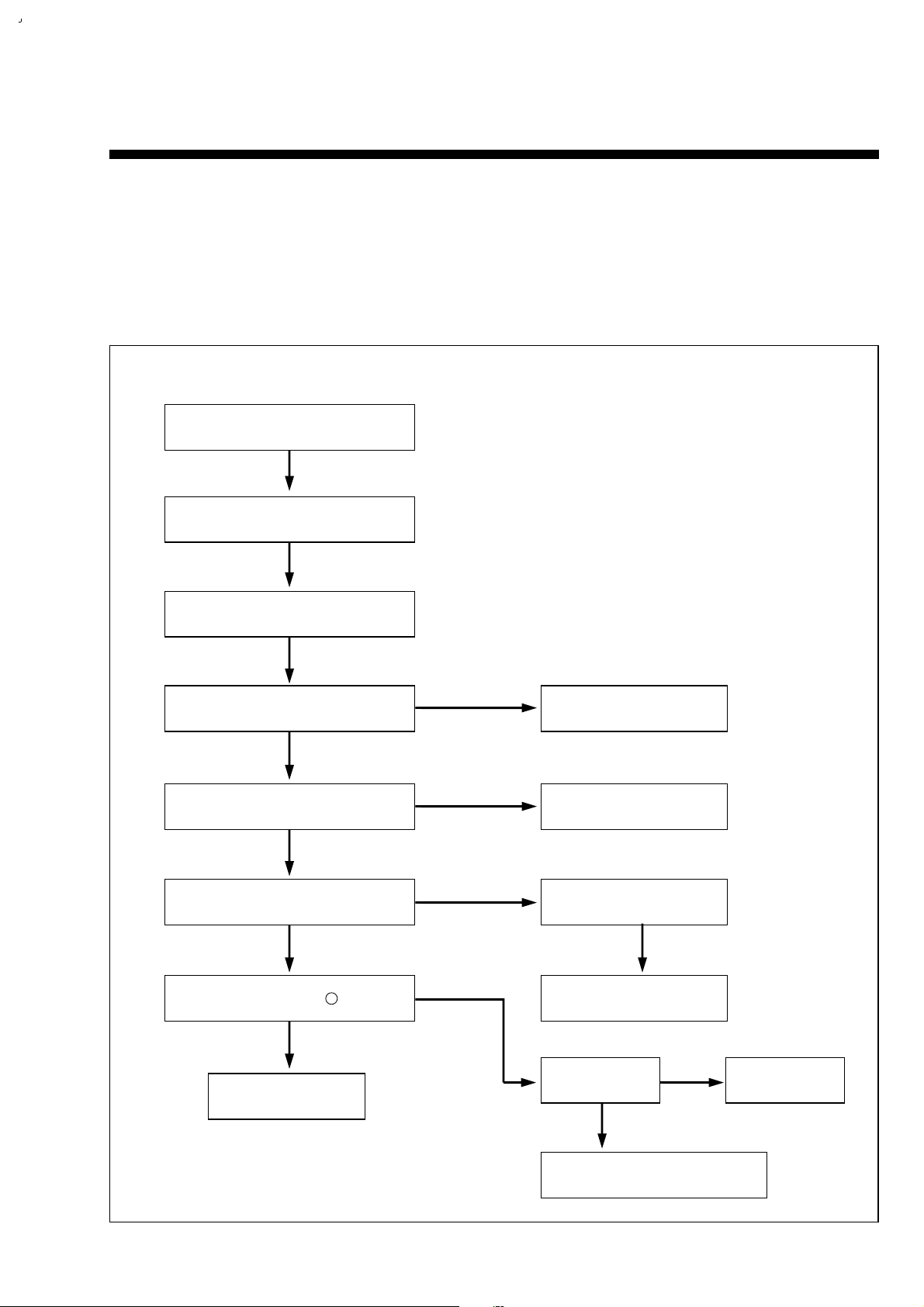
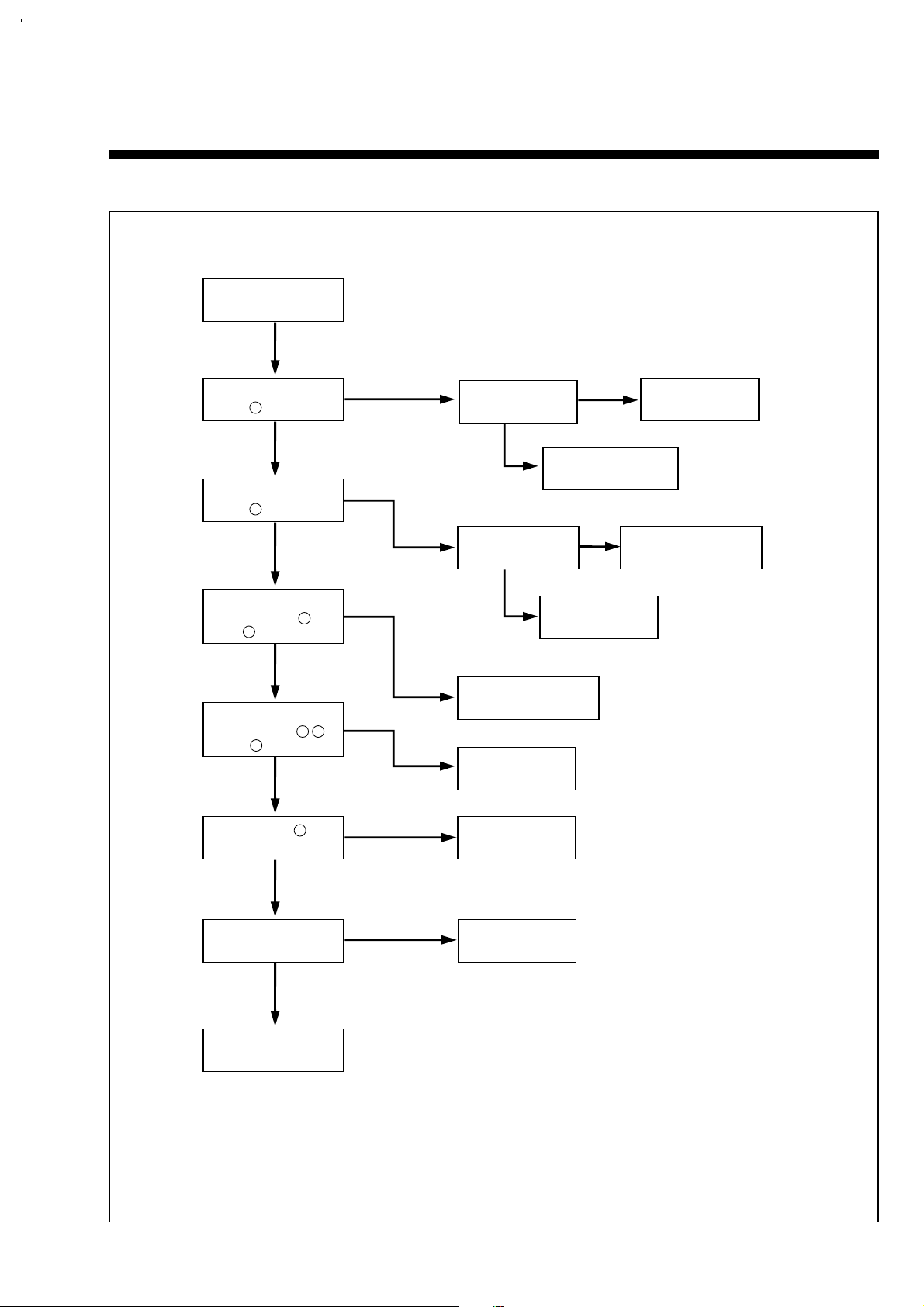
SECTION 3. TROUBLE SHOOTING FLOW CHART
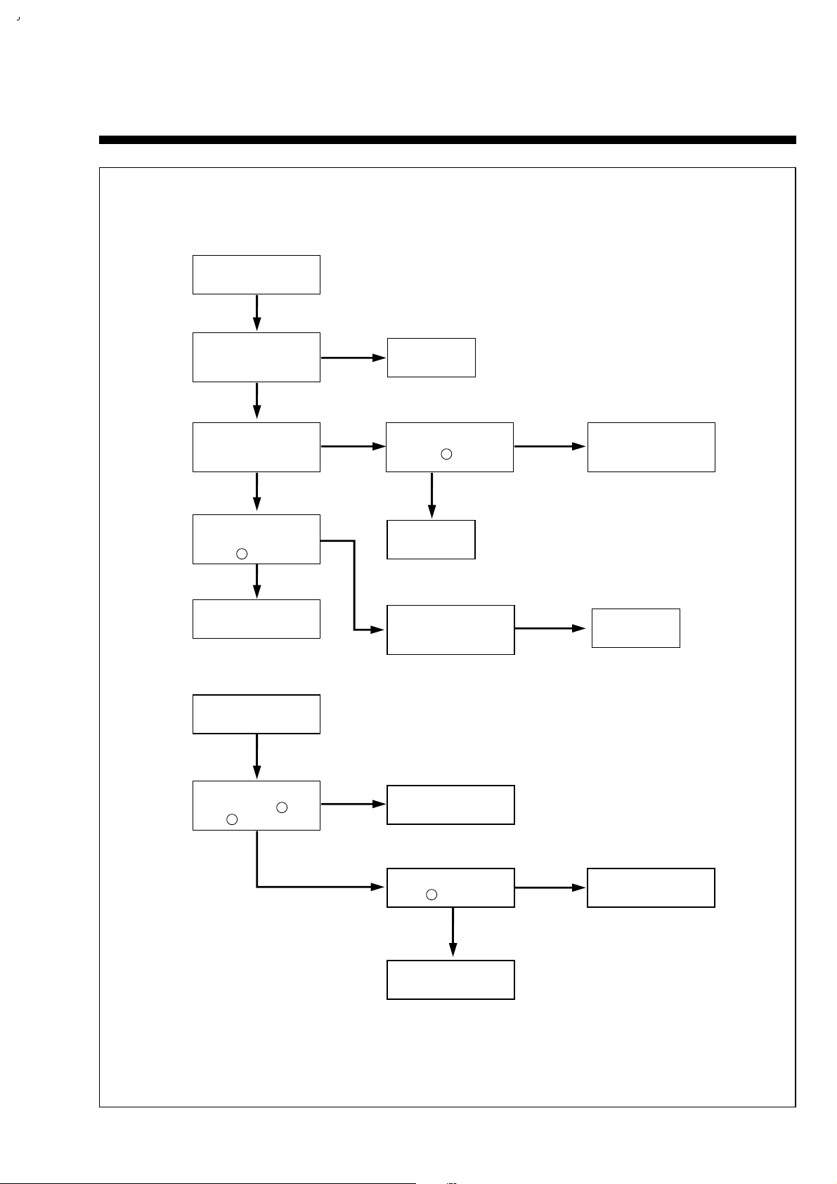
3-1. POWER CIRCUIT
• When change the parts which are out of order, first, remove the power plug from the socket and then discharge the
voltage across between both terminals of C807. (Use an external scores of KΩresistance)
• When check the primary circuit by using the oscilloscopes insulate the oscilloscope surely. (Use the isulating
transformer) and must connect GND into the primary GND), (But there is no connection when check the secondary
circuit).
• When change IC801, check FUSE and Cement resistance surely.
11
Prepare the instrument
connecting the insulating trans.
Check F801 FUSE.
Is voltage applied to D801?
Is voltage applied to the
both terminals of C807?
Check voltage of Q801 Gate.
4
Is voltage output from pin of IC801?
Check Q801.
Check D801, L801 & L802.
Check R802.
Check R803, 805,
814 & 806.
Check Q802, 803,
D802.
Check IC801. Change IC801.
Check the Secondary circuit.
NO
NO
NO
NO
NO
YES
YES
YES
YES
YES
YES
YES
YES
NO output Voltage.
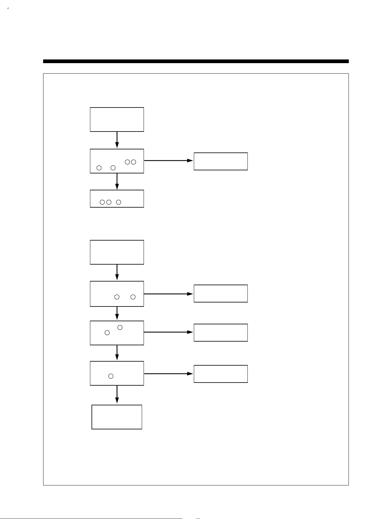
A. CHECKING THE PRIMARY CIRCUIT.
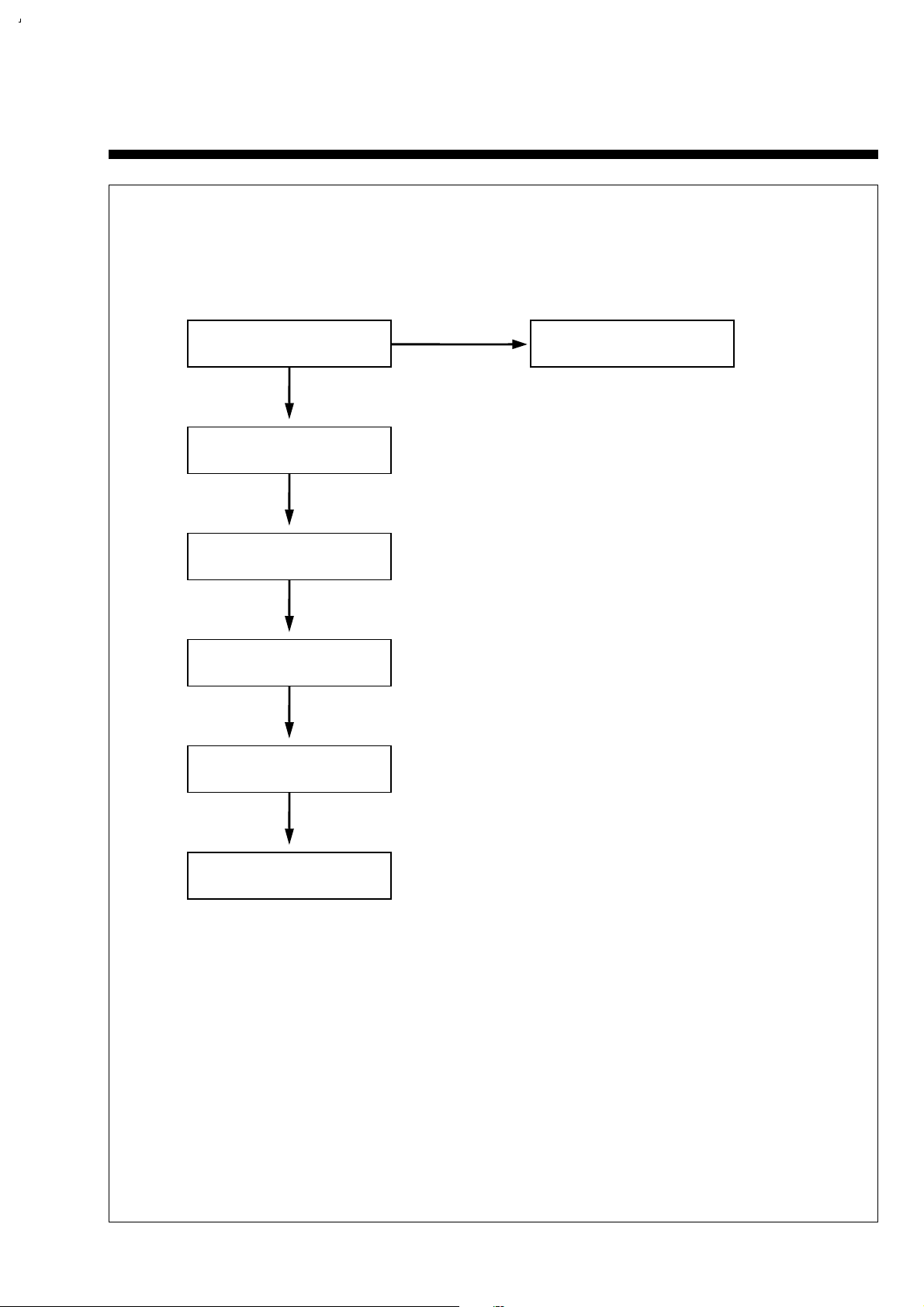
12
IS D811 Short?
Check each votage.
Check Trans output of
No output stage.
Check the DIODE of
NO output stage.
Check COIL, C of
No output stage.
Check the environmental
terminals of IC801.
Change D811 and check
IC801 and primary circuit.
YES
NO
YES
YES
YES
YES
B. CHECKING THE SECONDARY CIRCUIT.
3-2. LOGIC CIRCUIT
13
Digitron does
not operate.
Is+5V supplied to
pin of IC701?
8
Is-24V supplied to
pin of IC701?
11
Are -20 and -16.5V
supplied to pin and
of G701?
1
35
Are CLK signals
supplied to pin ,
and of IC701?
1 2
3
Is 5V at pin of
IC701?
7
Check X701.
Check IC701
and change.
Check the
Fuse of F802.
Is+5V supplied to
CATHOD of D712?
Is-28V at D614
anode?
Check D814 and
primary power circuit.
Change D614.
Check the Trans output
and D605.
Check IC601.
Change IC702.
Change X701.
YES
YES
YES
YES
YES
YES
NO
NO
NO
NO
NO
NO
NO
NO
YES
A.
YES
Check the connector
and pattern.
14
Digitron is lit but
key do
not operate.
Is each key pulse
applied to pin ,
and of IC701?
2 3
12 13
Check key matrix
circuit.
Check the pin serial of
pin , ~ of IC701.
65 67 69
It has not power-failure
compensation
operation.
When disconnecting
the power cord,is 3.6V
at pin and
of IC601?
26 81
Do pin and
of IC601
oscillate?
42
Is +5V applied to
pin of IC601?
37
Check IC601.
Check C629.
Check X602
environmental circuit.
NO
YES
YES
YES
YES
NO
NO
NO
B.
C.
43
Check the IC606
RESET circuit.
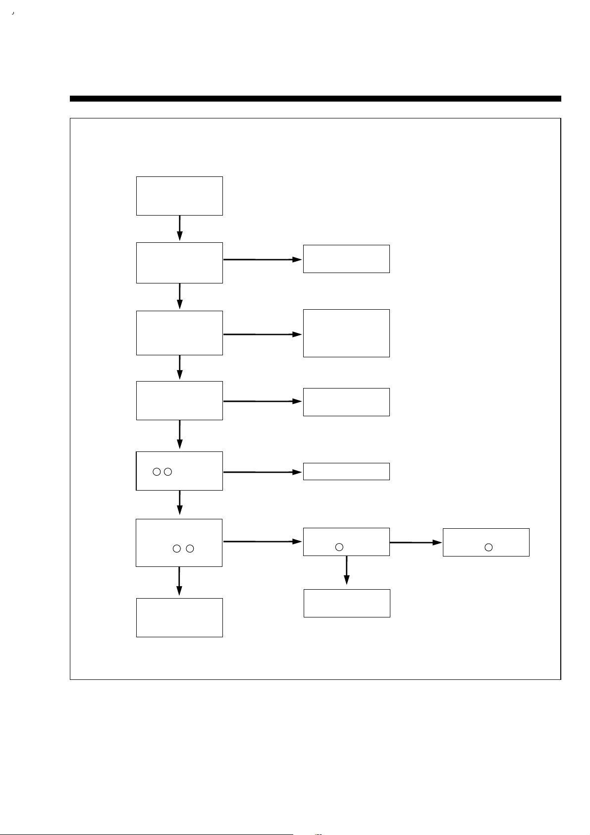
15
When change the
channel broadcast
signal is not received.
Is the external ANT.
connected to RF IN of
VCR and RF OUT
of TV?
Is the Power of VCR
ON and the VCR
indicator lit on the
digitron?
Does the TV channel
correspond to VCR
(3 or 4) channel?
Change and check the
connection of CABLE
Power On and select
the VCR mode by
pressing the
TV/VCR key.
YES
YES
YES
YES
NO
NO
NO
D.
Set the TV channel to
VCR (3 or 4) channel.
Check the Video,
Audio outputsignal of
pin , of
TMI BLOCK.
Check the TMI
BLOCK.
Check IC601
Check the
Video circuit.
Check the
IC601 pin.
Is the output of pin
, of IC601
normal?
100 98
YES
NO
44
14 18
Is the signal applied
to pin of IC151?
NO
YES
NO
YES
14
16
91
The voltage of pin
of IC601 is not
changed.
Is CTL pulse input
to pin and of
IC601?
71 72
73
Check and
re-adjust the
Path of Deck.
Check circuit
adjacent to IC601.
Check R523, R524
C508, C509.
check R518
and C511.
Check IC601.
YES
YES
YES
YES
YES
YES
YESNO
NO NO
NO
NO
NO
A.
Playback picture
is not good.
Noise appears
although adjusting
tracking.
Is CTL pulse applied
to pin of IC601?
Noise shakes up
and down on the
screen.
Adjust
tracking.
CTL HEAD height is
normal and there is
not dust.
Adjust the HEAD
height and remove
dust.
Noise appears
although change
cassette tape.
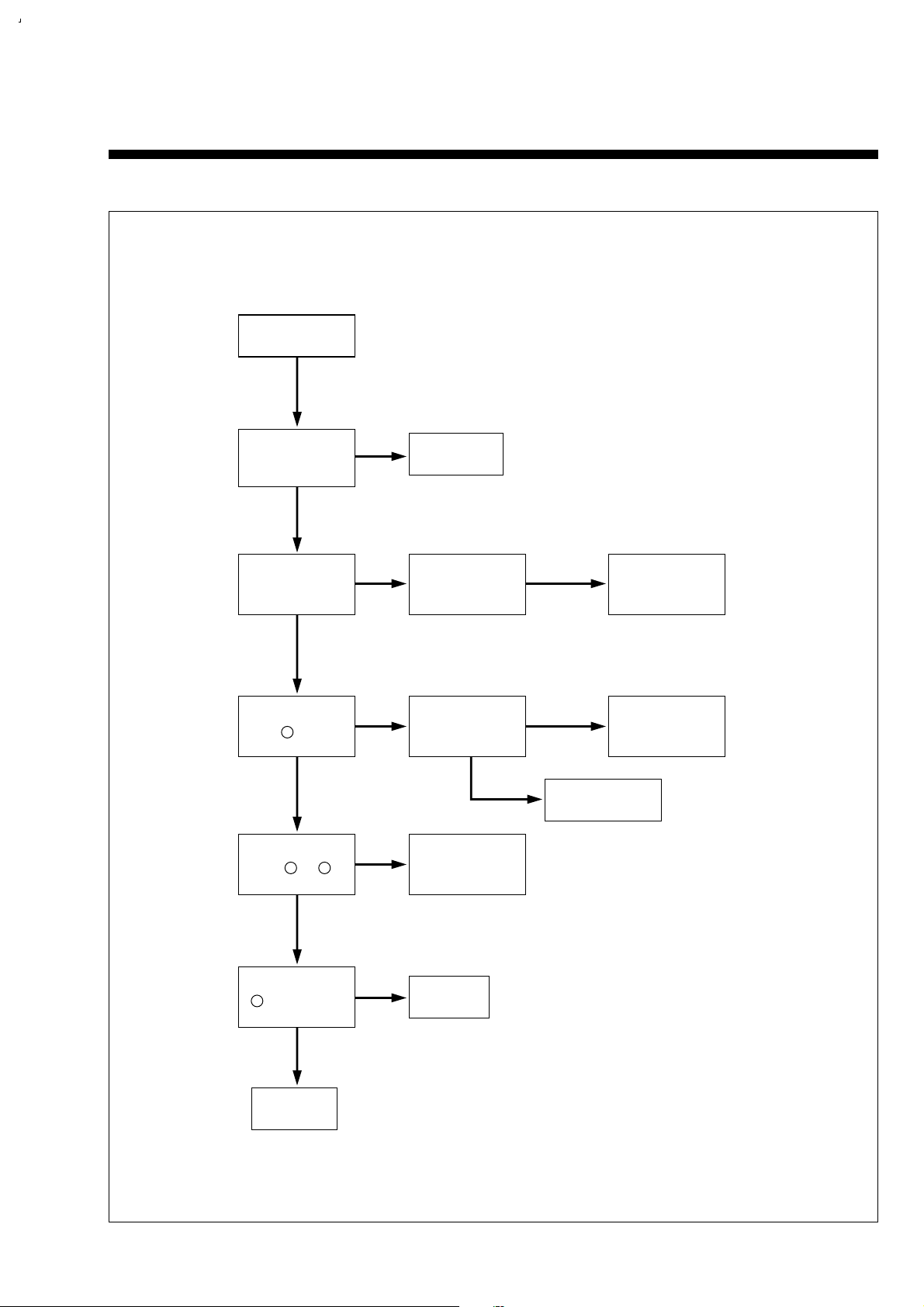
3-3. SERVO/SYSCON CIRCUIT
17
Playback picture
is not good.
Noise appears
on the screen
whole.
Is Enve.waveform
supplied to at
pin of PT01?
4
Are SW pulse and
HA SW applied to
HEAD-AMP circuit?
Check VIDEO circuit.
Auto stop during
playback.
Is Reel pulse
applied to pin and
of IC601?
5
6
Check Flow A.
Is SW pulse supplied
from pin of IC601?
16
Check D.PG input
and connector.
Check pattern.
Check connector, Head
Amp and Head dust.
Change Head.
Check REEL
sensor part.
Is D.FG applied to
pin of IC601?
Check connector
and D.FG circuit.
Check IC601.
NO
YES
YES
YES
YES
YES
NO NO
NO
NO
NO
YES
NO
10
B.
C.
 Loading...