

Page 1

Caution
: In this Manual, some parts can be changed for improving. their
performance without notice in the parts list. So, if you need the
latest parts information, please refer to PPL(Parts Price List)in
Service Information Center.
Service Manual
42" PLASMA PDP TV
CHASSIS :
Model :
S/M NO. : DSP201PEF0
SP-201P
DPP-4272NBS
Page 2
Contents
I. Parts with the exception of MODULE
1. Safety Precautions 2
2. Product Specification 3
2-1. SPECIFICATION 3
2-2. Available Input Signal 5
2-3. Remote Control Setup Code 6
3. BLOCK DIAGRAM 27
4. Description Of A/V and power 28
4-1. Block Diagram of main IC and TP 28
4-2. Overview 29
4-3. POWER PCB 37
4-4. Interface with PDP module 39
5. SERVICE MODE 40
5-1. Checking initial menu data 40
5-2. Entering SERVICE MODE 41
5-3. Description Of SERVICE MODE Items 43
6. Adjusting Method 46
6-1. WHITE BALANCE Adjusting 46
6-2. POWER PCB Adjusting 47
7. SOFTWARE UPGRADE Method 49
8. Main PCB Trouble Diagnosis 52
8-1. MAIN & SUB PCB Trouble Diagnosis 52
8-2. POWER PCB Trouble Diagnosis 59
9. TROUBLE DIAGNOSIS 60
9-1. Facts You Must Know When Diagnosing And Repairing 60
9-2. Typical Symptoms of PCB problem or bad Connection 60
9-3. Trouble Diagnosis and Repairing Method for Representative Symptoms 61
10. ASSEMBLY LIST 66
11. STRUCTURE OF PDP SET 67
12. EXPLODED VIEW 72
II. Parts of MODULE
1. Confirmation Manual
2. Repair Manual
-1-
Page 3
-2-
1. Safety Precautions
I. Parts with the exception of MODULE
1. Safety Precautions
(1) When moving or laying down a PDP Set, at least two people must work together. Avoid
any impact towards the PDP Set.
(2) Do not leave a broken PDP Set on for a long time. To prevent any further damages, after
checking the condition of the broken Set, make sure to turn the power (AC) off.
(3) When opening the BACK COVER, you must turn off power (AC) to prevent any electric
shock. When PDP is operating, high voltage and high current inside the Set can cause
electric shocks.
(4) When loosening screws, check the position and type of the screw. Sort out the screws and
store them separately for reassembling. Because screws holding PCBs are working as
electric circuit GROUNDING, make sure to check if any screw is missing when
assembling/reassembling. Do not leave any screws inside the set.
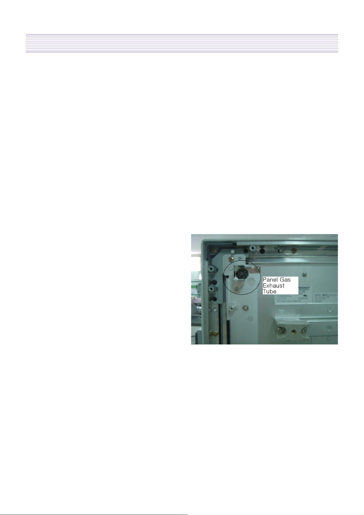
(5) If you open the BACK COVER, you will see a
Panel Gas Exhaust Tube (Picture. 1-1) inside
the bracket. If this part is damaged, the entire
PDP PANEL must be replaced. Therefore,
when working with the set, be careful not to
damage this part.
Picture 1-1. Panel Gas Exhaust Tube
(6) A PDP Set contains different kinds of
connector cables. When connecting or disconnecting cables, check the direction and
position of the cable beforehand.
(7) Connect/disconnect the connectors slowly with care especially FFC (film) cables and FPC
cables. Do not connect or disconnect connectors instantaneously with force, and handle
them carefully for reassembling.
(8) Connectors are designed so that if the number of pins or the direction does not match,
connectors will not fit. When having problem in plugging the connectors, check their kind,
position, and direction.
Page 4
-3-
2. Product Specification
I T E M S P E C I F I C A T I O N REMARK
1. GENERAL
1-1. MODEL NO DPP-4272NBS
1-2. CHASSIS NO SP-201P
1-3. SCREEN SIZE 42” (16:9)
1-4. COUNTRY Europe
1-5. RESOLUTION 853(H) x 480(V)
1-6. REMOCON TYPE R-52M17
1-7. SAFETY STANDARD CE(CLASS B), CB
1-8 .TUNIG METHOD FS
1-9. MEMORY CHANNEL 99CH
2. MECHANICAL
2-1. APPEARANCE
1) WITHOUT STAND W x H x D =1044 x 631 x 89 mm
2) WITH STAND W x H x D =1044 x 705.9 x 310 mm
2-2. WEIGHT
1) WITHOUT STAND 30.2 Kg
2) WITH STAND 37 Kg
3. ELECTRICAL
3-1. VIDEO INPUT COMPOSITE(NTSC, PAL, SECAM, PAL-M/N, NTSC4.43) &
S-VHS(50/60Hz Y/C) 1 set
3-2. DTV/DVD INPUT 1080 i, 720P, 480P , 480i, 576P, 576i
(Y, Pb/Cb, Pr/Cr COMPONENT SIGNAL) 2sets
3-3. SCART INPUT SCART(COMPOSITE, R,G,B, SOUND) R/L 2sets
3-4. PC INPUT VGA ~ SXGA(Dot clock : 120MHz), 15 PIN D-SUB 1set
3-5. DVI INPUT DVI-D INPUT (DVI Jack) 1set
3-6. TV INPUT
1) COLOR STANDARD PAL B/G+I/I+D/K, L-SECAM, L’--SECAM
2) ANTENNA IN ONE INPUT 75
Unbalanced (DIN Standard)
3) RECEPTION CHANNEL
VHF LOW : E2 ~ S6 Ch.
VHF HIGH : S7 ~ S36 Ch.
UHF : S37 ~ E69 Ch.
L’-SECOM : FB, FC1, FC
4)
IF & SUBCARRIER
PIF : 38.90MHz (PAL B/G+I/I+D/K, L-SECAM
33.9 MHz (L’-SECAM)
SIF : 33.40MHz (B/G), 32.90MHz (I/I),
32.4MHz (D/K, L-SECAM), 40.4MHz (L’--SECAM)
3-7. SOUND INPUT VIDEO 1set, DTV/DVD 2set, PC 1set, DVI 1set
3-8. SPEAKER OUTPUT 10W(R) + 10W(L)
3-9. POWER REQUIREMENT AC 100V~240V, 50/60Hz
2-1. SPECIFICATION
Page 5
-4-
Product Specification
I T E M S P E C I F I C A T I O N REMARK
3-10. POWER CONSUMPTION 260W(Typical)
3-11. RS-232 CONTROL RS-232 Communication (FOR SERVICE UPGRADE)
3-12. AV OUTPUT SCART(CVBS, SOUND R/L) 2 sets
3-11. AV OUTPUT CVBS 1 set, SOUND R/L 1 set
3-13. FUNCTION
1) SCALING DVI : H/V SIZE
PC: H/V SIZE, POSITION, PHASE, FREQUENCY
VIDEO/DVD(480i/576i) : 16:9, 4:3, AUTO, EnlargeLB,
EnlargeLBS, PANORAMA
DTV/DVD(480P and Better Reolusion) : 16:9, 4:3
2) ZOOM 20 STEP ZOOM and PANING
3) OSD Language
18 Languages (English, Greek, Dutch, German, Russian, Rumanian,
Swedish, Danish, Finnish, Norwegian, Spanish, Italian, French,
Polish, Portuguese, Czech, Hungarian , Slovakian)
4) OTHERS STILL, SLEEP MODE, SOUND MODE, PICTURE MODE
TIMER, TELETEXT (LEVEL 2.5)
4. OPTICAL
4-1. SCREEN SIZE 42”(106 cm) DIAGONAL
4-2. ASPECT RATIO 16 : 9
4-3. NUMBER OF PIXELS 853(H)X480(V)
4-4. DISPLAY COLOR 1,677 Million Colors ( 8bits for each RGB)
4-5. CELL PITCH 1.08(H) x 1.08(V)mm (1 Pixel = a Set of RGB Cells )
4-6. PEAK LUMINANCE 400cd/m
2
(WITH FILTER GLASS)
4-7. CONTRAST RATIO 1500:1 (Dark Room)
4-8. VIEWING ANGLE 160 degree(VERTICAL/HORIZONTAL)
5. USERCONTROL & ACCESSORIES
5-1 CONTROL BUTTON(SET) PUSH-PULL S/W : AC POWER BUTTON
SOFT S/W: MOVE/CH(UP, DOWN), VOLUME(LEFT, RIGHT),
MENU, INPUT SELECT
5-2. REMOTE CONTROL
(R-52M17) Power, Universal Selection (TV, VIDEO/DVD, CATV/SAT),
10 KEYS(0~10), Recall, VCR /DVD KEY
(F.R/SLOW, Play, F.F/SLOW, Stop, PAUSE, OPEN/CLOSE,
PREV, NEXT ), Menu, TV/VIDEO, MULTIMEDIA, Still,
Previous PR, Sound Off, PR(UP/DOWN), Volume(UP/DOWN),
P.MODE, S.MODE, - , Screen Size, Zoom-, Zoom+, Sleep Timer,
Multilingual/CYAN, Sound Mode/INDEX,. RED, GREEN, YELLOW,
TEXT, REVEAL, UPDATE, EXPAND, SUBPAGE, HOLD
5-3. ACCESSORIES
REMOCON, BATTERY, USERS MANUAL, A/V CABLE, RF CABLE
5-4. OPTIONAL PARTS STAND, WALL HANGER, SPEAKER UNITS(Left, Right)
Page 6
-5-
Product Specification
Resolution H Freq. (KHz) V Freq. (Hz) Remark DVI PC
640x400 37.861 85.080 VESA O
640x480 31.469 59.940 DOS O O
37.861 72.809 VESA O O
37.500 75.000 VESA O O
43.269 85.061 VESA O O
720x400 31.469 70.087 IBM O O
37.927 85.039 VESA O
800x600 35.156 56.250 VESA O O
37.879 60.317 VESA O O
48.077 72.188 VESA O O
46.875 75.000 VESA O O
53.674 85.061 VESA O O
1024x768 48.363 60.004 VESA O O
56.476 70.069 HP&VESA O O
60.023 75.029 VESA O O
68.677 84.997 VESA O
1152x864 67.500 75.000 VESA O O
1280x960 60.000 60.000 VESA O O
2-2. Available Input Signal
(1) PC & DVI
(2) DTV
-1080i/ 60 Hz
-720P / 60 Hz
-480P / 60 Hz
(3) VIDEO
-PAL, PAL-M, PAL-N
-NTSC , NTSC4.43
- SECAM
Page 7
-6-
Product Specification
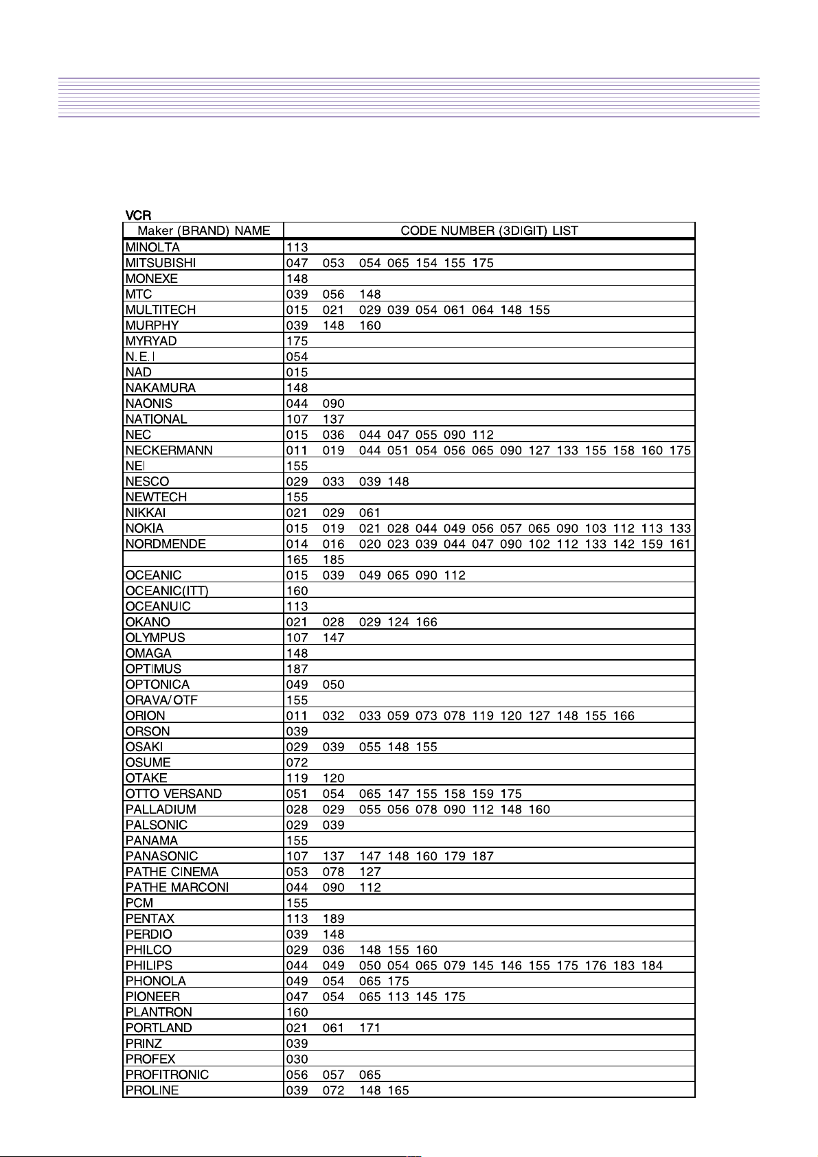
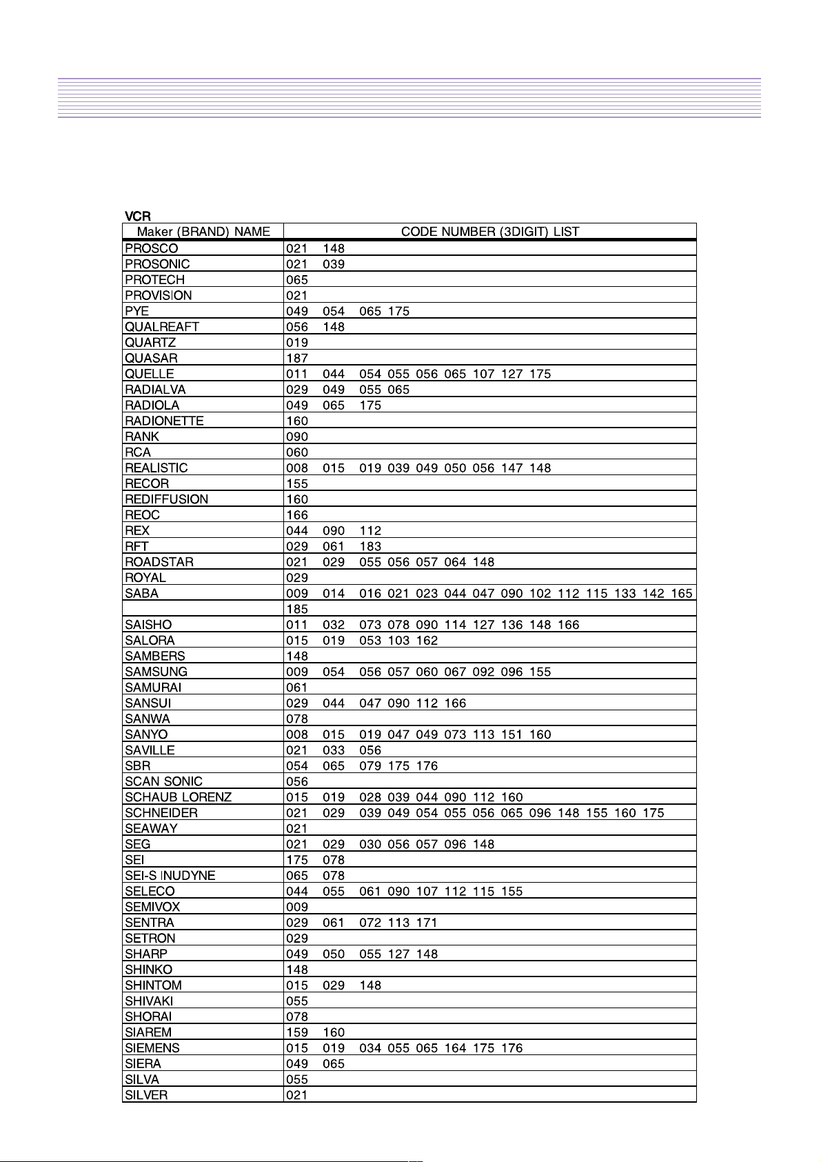
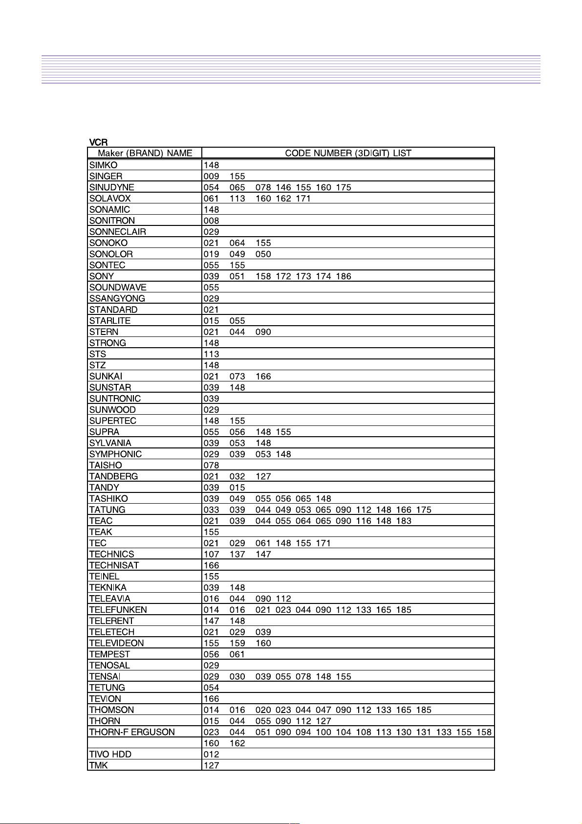
2-3. Remote Control Setup Code
Page 8
-7-
Product Specification
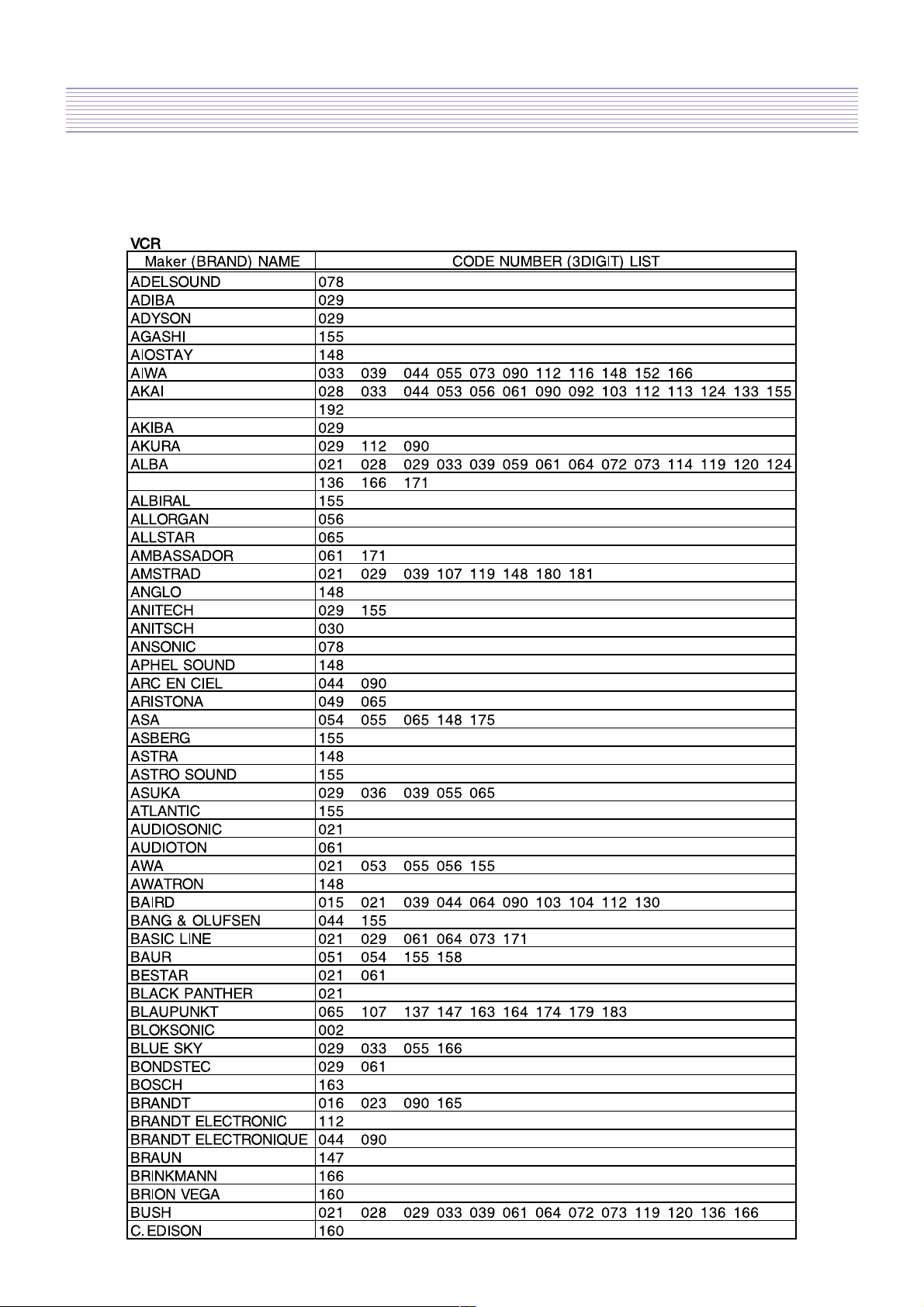
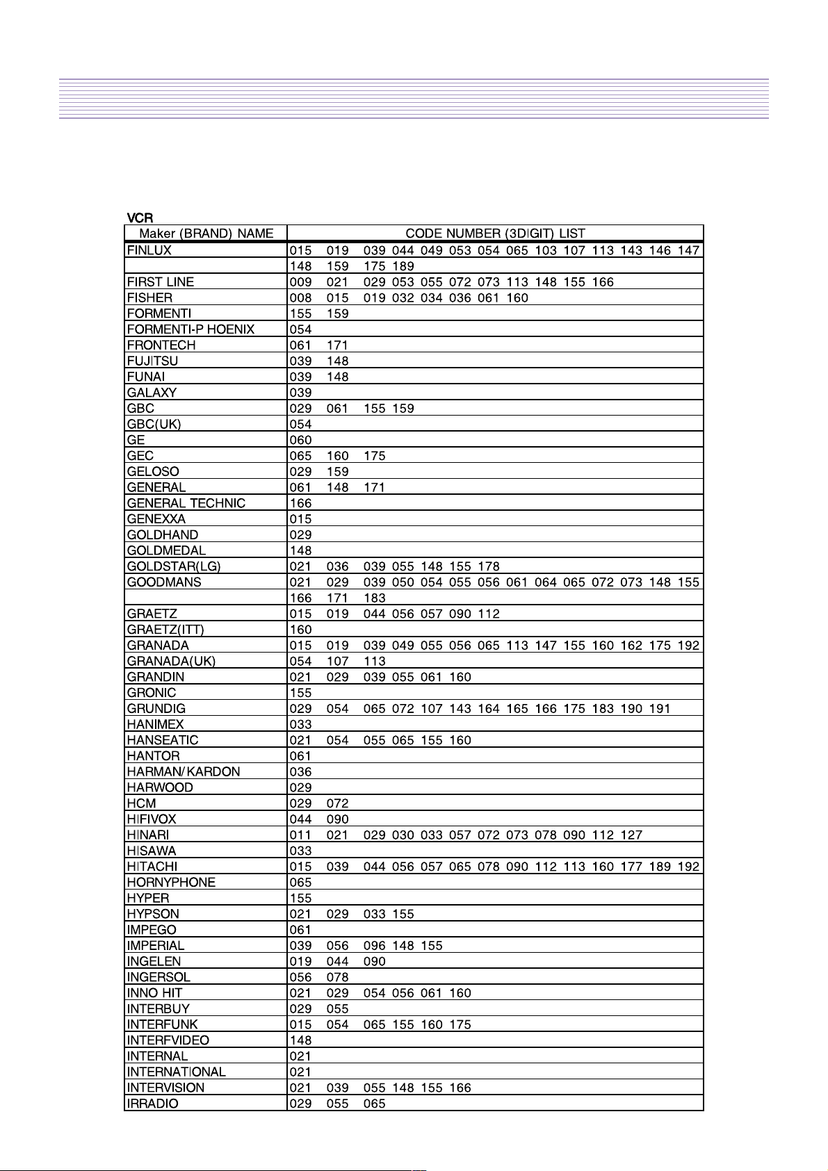
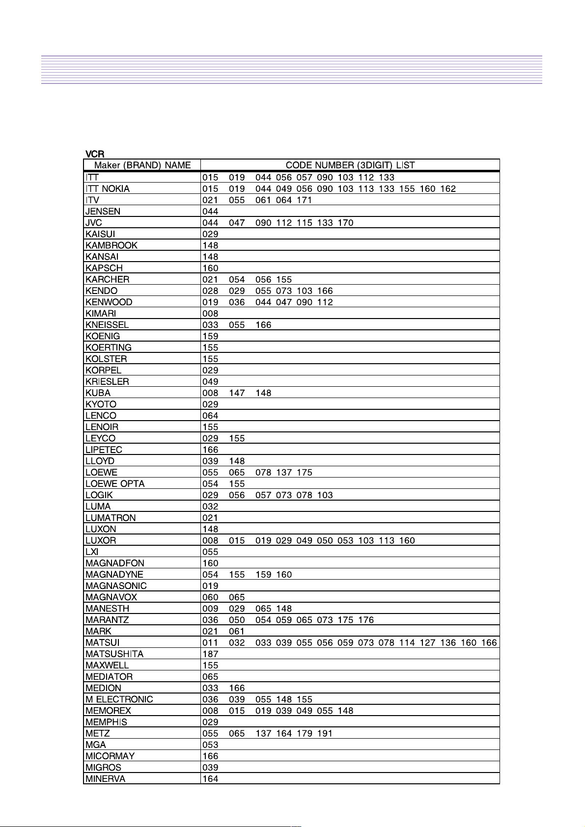
VCR
VCRVCR
VCR
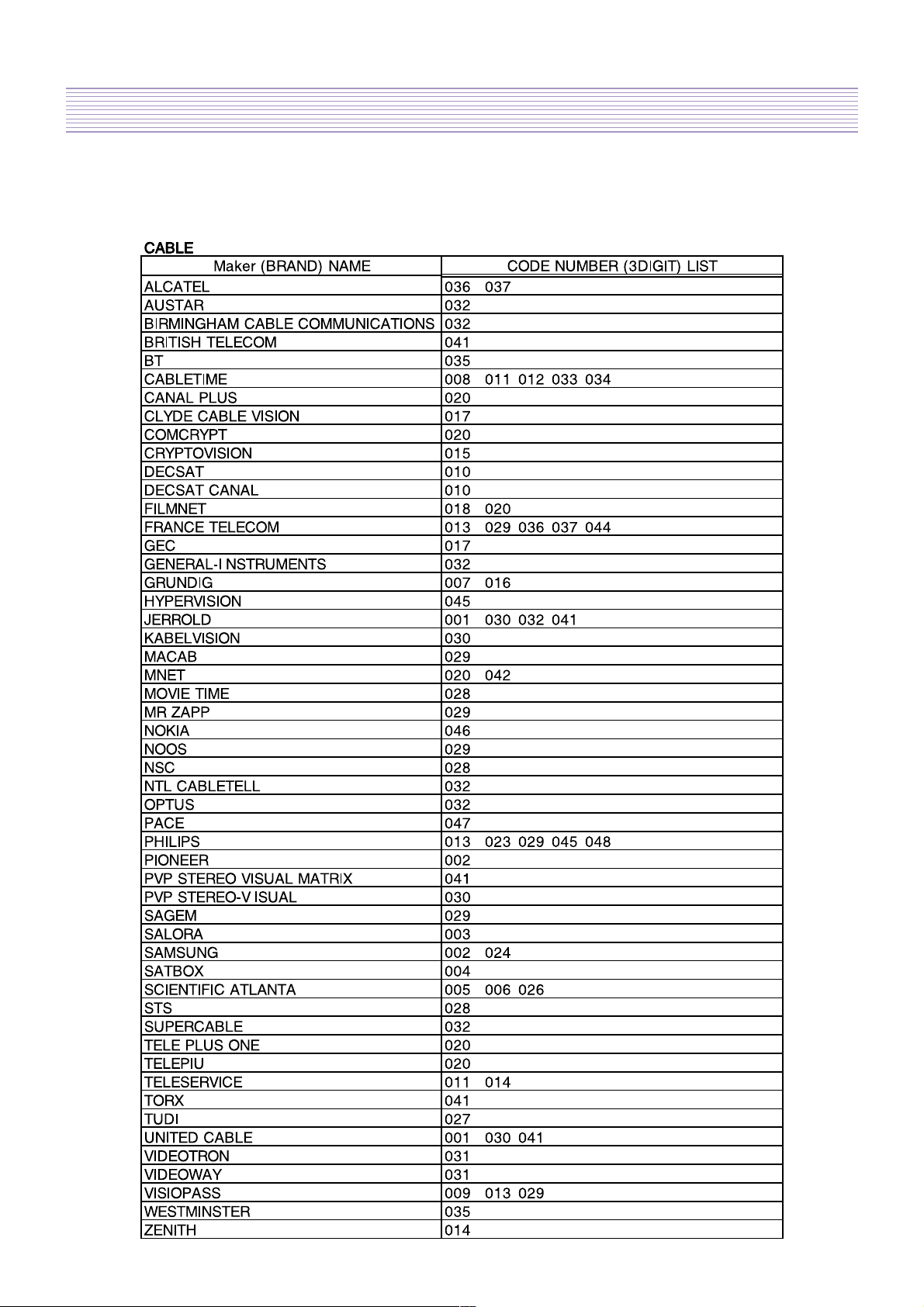
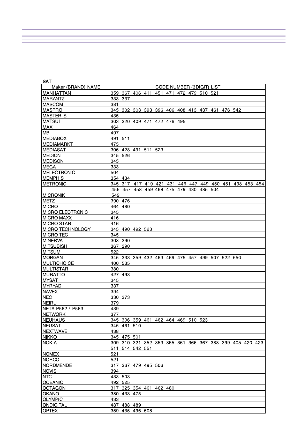
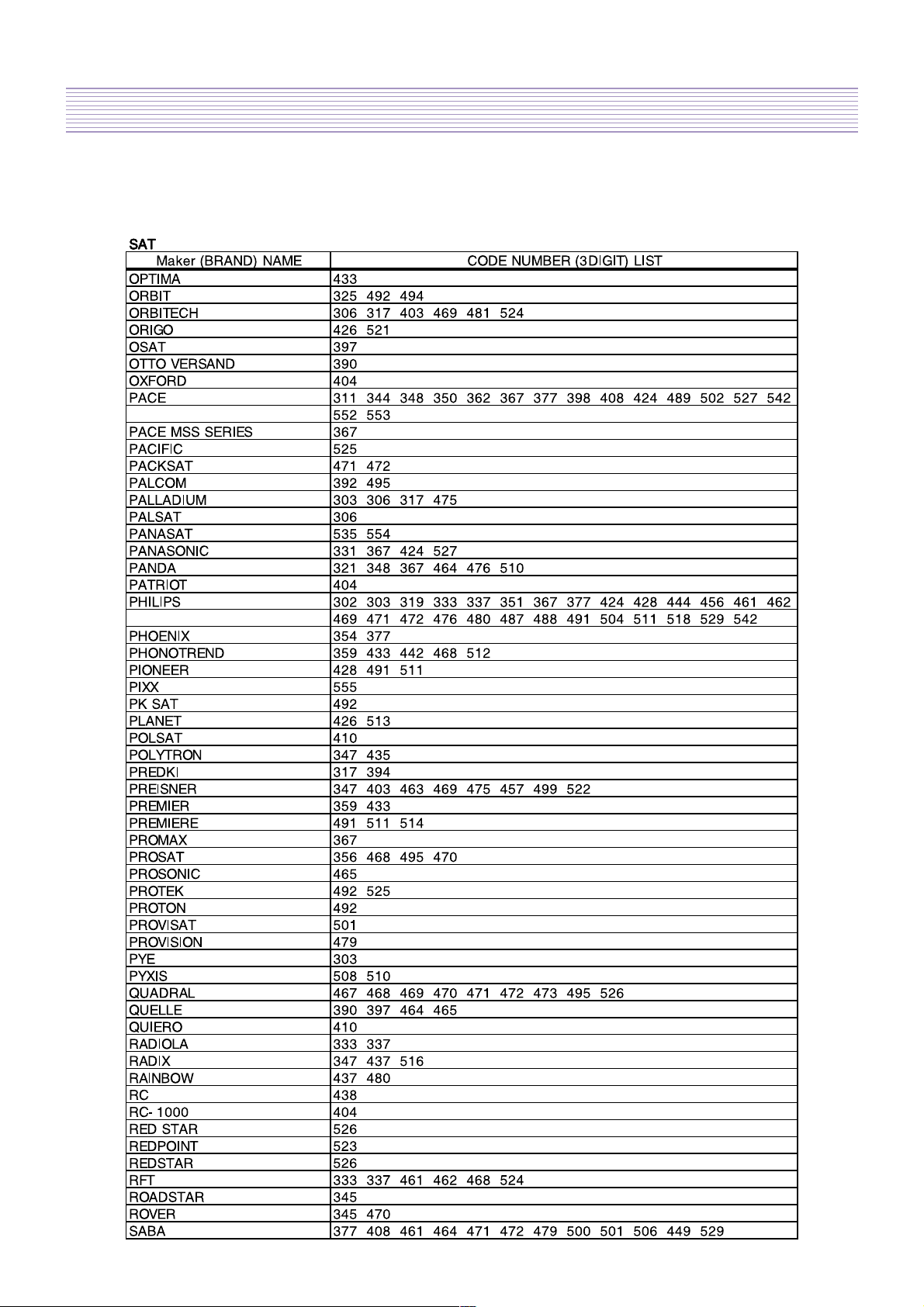
Mak er (BRAND) NAME CODE NUMB ER ( 3D IGIT) L IST
CANON 147
CAPEHART 061
CARENA 065
CARREFOUR 009
CASIO 039 148
CATHAY 021
CATRON
061 171
CGE 039 044 090 133 148 155
CIHAN CLARIVOX 1 55
CIMLINE
029
CLATRONIC
029 061 171
COMBITECH
033
CONDOR 021 061 155 171
CONTI NEN TA L ED ISO N 044 090
CORVUS 148
CRAIG 008 056
CROSLEY 160
CROWN 009 021 029 061 064 171
CROWN/ONWA 148
CURTISMATHES 060
CYRUS 175
DAEWOO 001 009 021 033 061 064 155 171
DANSAI 021 029 055
DAWA 155
DAYTRON 021 061
DE GRAAF 113 177
DECCA 039 044 047 065 090 148 155 166 175
DECCA(UK) 054
DEGRAAF 015 039 049 054 065 113 148
DEITRON 021
DENKO 029
DENON 113
DESMET 155
DIAMANT 055
DIXI 078
DOMOH 155
DORIC 160
DUAL 021 039 044 065 090 112 148 155
DUMONT 015 039 054 065 148 155 175 189
DYNATECH 039 148
ELBE 021 036 148
ELCATECH 029
ELIN 056 113 155
ELSAY 029
ELTA 021 029 148
EMERSON 009 011 029 032 039 060 073 127 148 155
ESC
021 056 057 061 064
ESSELTE 148
ETZUKO
029
EUROMAN 155
EUROPHON 061
FENNER 061 155
FERGUSON 016 021 023 039 044 090 094 100 104 108
112
130 131 165
FIDELITY 029 039 056 148 162
FINLANDIA 015 039 049 054 065 113 175
Page 9
-8-
Product Specification
Page 10
-9-
Product Specification
Page 11
-10-
Product Specification
Page 12
-11-
Product Specification
Page 13
Product Specification
-12-
Page 14
Product Specification
-13-
Page 15
Product Specification
-14-
Page 16
Product Specification
-15-
Page 17
Product Specification
-16-
Page 18
Product Specification
-17-
Page 19
-18-
Product Specification
Page 20
-19-
Product Specification
Page 21
Product Specification
-20-
Page 22
Product Specification
-21-
Page 23
Product Specification
-22-
Page 24

Product Specification
-23-
Page 25

Product Specification
-24-
Page 26

Product Specification
-25-
Page 27

Product Specification
-26-
Page 28

-27-
3. BLOCK DIAGRAM
Page 29

-28-
4. Description of A/V(MAIN and SUB PCB) and POWER
4-1. Block Diagram of main IC and TP
IC112
IC149
IC140
IC114
IC102
IC134
IC121
IC132
IC104
IC904
IC903
IC901
PC901
TUNER
LED
KEY
PC101
PC102
PC102
PC900
JA109
JP117
PA102
P100
TO PWR
TO PWR
TO PDP
MODULE
PC103
TP116
TP117
TP130
TP128
TP204 TP205
TP187
TP184
TP181
TP188
TP261
TP136
TP135
TP134
TP143
TP145
TP_AUDIO
Top
Bottom
IC126
IC156
JP118
JA110
Page 30

-29-
Description of A/V(MAIN and SUB PCB) and POWER
4-2. Overview
A/V block (Main and Sub PCB) is Multi Media circuit board that can process various input signals
such as video, component, PC, DVI, and analog TV signal. It is mainly composed of switching,
sync processing, decoding, analog TV, digital image processing, and system control part
4-2-1. Composite video, Y/C(S-Video) and SCART (CVBS, RGB) composite video
Y/C(S-Video) and SCART(CVBS) have similar signal paths, IC102 receives these signals
and swithes out a selected signal. Then the signal goes into IC132 for video processing,
SCART(RGB) signal goes directly into IC132. The output of IC132 goes through IC134 and
IC140 for deinterlacing and digital image processing respectively.
- Main IC
A. IC102: Switching IC (Input: analog inputs Output: an analog output)
B. IC126: Teletext IC
C. IC132: Video processor (Input: Y/C, CVBS Output: 16bit digital, HV)
D. IC134: Deinterlacer (Input: 16bit digital, HV Output: 24bit digital RGB, HV)
E. IC140: Image Processor (Input: 24bit digital RGB, HV Output: 24bit digital RGB, HV)
- Main TP (Input: Color Bar Pattern)
TP145: Brightness signal (input to IC132)
TP143: Color signal (input to IC132)
Page 31

-30-
Description of A/V(MAIN and SUB PCB) and POWER
TP184: Horizontal sync (output of IC140)
TP187: Vertical sync (output of IC140)
TP181: Data enable (output of IC140)
Page 32

-31-
Description of A/V(MAIN and SUB PCB) and POWER
4-2-2. TV signal
Tuner(PC901) receives antenna signal and outputs CVBS and sound signal. IC102 switches out the
CVBS and the rest of the signal flow is same as composite video signal flow mentioned earlier.
- Main IC
A. PC901: Tuner (Input: antenna signal Output: CVBS)
B. IC102: Switching IC (Input: CVBS Output: CVBS)
C. IC126: Teletext IC
D. IC132: Video processor (Input: Y/C Output: 16bit digital, HV)
E. IC134: Deinterlacer (Input: 16bit digital, HV Output: 24bit digital RGB, HV)
F. IC140: Image Processor (Input: 24bit digital RGB, HV Output: 24bit digital RGB, HV)
- Main TP (Input: Color Bar Pattern)
TP143, 145
TP181, 184, 187, 188
4-2-3. DTV/DVD signal
Both DTV(Y, Pb, Pr) and DVD(Y, Cb, Cr) share same jack and signal path. IC102 switches out
signal and also detects type of signal so that IC121 can convert the analog signal to digital. Then
the signal goes through IC134(deinterlacer) and IC140 for digital image processing.
- Main IC
A. IC102: Switching IC (Input: Component Output: Component, HV)
B. IC121: A/D converter (Input: Component, HV Output: 24bit digital RGB, HV)
C. IC134: Deinterlacer (Input: 24bit digital RGB, HV Output: 24bit digital RGB, HV)
D. IC140: Image Processor (Input: 24bit digital RGB, HV Output: 24bit digital RGB, HV)
TP188: Clock for display (output of IC140)
Page 33

-32-
Description of A/V(MAIN and SUB PCB) and POWER
- Main TP (Input: 480P, Color Bar Pattern)
TP261: Y signal (Input to IC121)
TP134: Clock (output to IC121)
TP135: Horizontal sync (output of IC121)
Page 34

-33-
Description of A/V(MAIN and SUB PCB) and POWER
4-2-4. PC (Personal Computer)signal
PC signal is switched out by IC109 and input to IC114 for A/D conversion. Then the signal goes
through IC140 for digital image processing.
- Main IC
A. IC109: Switching IC (Input: Analog RGB, H, V Output: Analog RGB, H, V)
B. IC114: A/D converter (Input: Analog RGB, H, V Output: 24bit digital RGB, H, V)
C. IC140: Image Processor (Input: 24bit digital RGB, H, V Output: 24bit digital RGB, H, V)
- Main TP (Input: Color Bar Pattern)
TP130: Vertical sync (output of IC114)
TP136: Vertical sync (output of IC121)
Page 35

-34-
Description of A/V(MAIN and SUB PCB) and POWER
TP128: SYNC for PLL (output of IC114)
TP127: Output clock (output of IC114)
4-2-5. DVI(Digital Visual Interface) signal
To process DVI signal, graphic card of AV device reads EDID data from IC101(ROM). Then DVI
signal is directly inputted to IC112, which outputs digital 24bit RGB and H, V. The output goes
through IC140 for digital image processing.
- Main IC
A. IC101: ROM containing EDID data (EDID: display capabilities such as resolution, aspect ratio
etc.)
B. IC112: DVI signal processor (Input: TMDS Output: 24bit digital RGB, H, V)
Page 36

-35-
Description of A/V(MAIN and SUB PCB) and POWER
- Main TP (Input: Color Bar Pattern)
TP116: Horizontal sync (output of IC112)
TP117: Vertical sync (output of IC112)
4-2-6. Video Enhancer and LVDS transmitter (for all inputs)
Outputs of IC140 are inputted to IC149(video signal enhancer) which improves picture quality greatly.
Outputs of IC149 are inputted to IC150 which is a LVDS transmitter. The converted LVDS signal is
transmitted to the digital board.
- Main IC
A. IC149: Video enhancer (Input: 24bit digital RGB, H, V Output: 24bit digital RGB, H, V)
B. IC150: LVDS transmitter (Input: 24bit digital RGB, H, V Output: LVDS signal)
- Main TP (Input: Color Bar Pattern)
TP204: Horizontal sync (output of IC149), refer to TP184
TP205: Vertical sync (output of IC149), refer to TP187
Page 37

-36-
Description of A/V(MAIN and SUB PCB) and POWER
4-2-7. Audio signal processing, KEY, and LED
IC104 switches Audio signals and passes a switched signal to IC904 for audio signal processing.
IC904 controls sound parameters such as Volume, Balance, and Equalize. The outputs of IC904 are
passed to IC901(left), and IC903(right) respectively to amplify the signals. KEY and LED PCBs send
signals received from key buttons and LED to IC140 for command processing.
- Main IC
A. IC104
B. IC904
C. IC901, IC903
- Main TP (Input: Sound wave 400Hz)
TP_AUDIO: AUDIO SIGNAL that goes into MSP3420 before AUDIO PROCESSING
RIGHT (LEFT) : AMP input signal before 30dB amplification
Page 38

-37-
Description of A/V(MAIN and SUB PCB) and POWER
Remote control signal
4-3. POWER PCB
<Input requirements>
Nominal Input Voltage: AC100V to AC240V (Variation Range- AC85V~ AC276V)
Single-Phase full wave
Regulation Method: Transistor & Switching Method
Input Frequency: 50~60Hz (Variable Range- 45Hz ~ 66Hz)
Inrush Current: 50A zero-peak max at AC264V
Output Voltage is as follows.
No. Output Nominal Variable Voltage Nominal Load current Ripple/Noise
Name Voltage Range Accuracy current range (mVp-p)*2
(V) (V) (%)*1 (A) (A)
1 Vsus 190 180-195 5V 1.3 0.1~1.3 1000/500
2 Vadd 60 50-80 2V 1 0.1~1 250/500
3 V1 5.1 - 5% 2.5 0.1~3 50/100
4V3 17 - 5% 1 0~1 50/100
(SOUND) -17 - 5% 1 0~1 50/100
5V4 50 - 5% 1.5 0.1~1.5 50/100
6V5 12 - 5% 0.6 0~1 50/100
7 Vstb 5 -
5% 1.5 0~1.5 100/100
Page 39

-38-
Connector number P4 P5 P7
Model name YMW025-10R YMW025-05R YMW025-04R
Maker YEONHO YEONHO YEONHO
The number of pins 10 5 4
1 NC POWER(ON/OFF) V3 - 17V
2NCNCG
3 V5 12V NC G
4 G G V3 17V
5 G Vstb
6 V4 5V
7G
8G
9NC
10 NC
Pin
number
* P2 is connected to P5 of Y-SUB PCB.
P3 is connected to P1 of Z-SUS PCB.
P6 is connected to P6 of Y-SUS PCB.
P4 is connected to PA4 of VIDEO PCB.
P5 is connected to PA5 of VIDEO PCB.
P7 is connected to PA6 of JACK PCB.
Description of A/V(MAIN and SUB PCB) and POWER
Connector number P2 P3 P6
Model name GP390-10P-TS 1-1123723-8 GP390-04P-TS
Maker LG Cabel AMP LG Cable
The number of pins 10 8 4
1 Vsus 190V Vsus 190V G
2 Vsus 190V Vsus 190V G
3 Vsus 190V NC V1 5.1V
4 NC G V1 5.1V
5GG
6 G Vadd 60V
7GG
8 G V1 5.1V
9NC
10 NC
Connector
Pin
number
Page 40

-39-
Description of A/V(MAIN and SUB PCB) and POWER
4-4. Interface with PDP Module
< PDP Module >
A/V
POWER
Page 41

-40-
5. SERVICE MODE
5.1 Checking initial menu data
(1) Check initial data of User Menu
1) Picture
- Mode : Normal
BRIGHTNESS : 32
CONTRAST : 48
COLOR : 32
Tint : 32 (CENTER) * Not displayed when input signal is PAL or SECAM
Sharpness : 32
- Colour Temp. : Normal
2) Sound
- Balance : 0 (CENTER)
- Effect : Off
- AVC : Off
- Mode : Normal
120 Hz : 0 (CENTER)
500 Hz : 0 (CENTER)
1.5 KHz : 0 (CENTER)
5 KHz : 0 (CENTER)
10 KHz : 0 (CENTER)
3) Screen Mode : 16:9
4) Features
- Background : Opaque
- Language : English
- Child Lock : Off
- Enhancer : On
- Auto Power : Off
- Time Setting
Clock : — —:—
Off Timer : Off
Off Time : AM 12:00
Wake Timer : Off
Wake Time : AM 12:00
Wake Pro. : 1
Wake Vol. : 20
- ISM
Pixel Shift : Off
Low Bright : Off
- Initialize
Page 42

-41-
SERVICE MODE
5) Install(TV input only)
- Auto Setup
- Edit
- Manual Setup
5-2 Entering SERVICE MODE
To enter SERVICE MODE
Press “ VOL” => “MUTE” => “RECALL” => “MUTE” BUTTON of Remote Controller
(1) Check initial data of Service mode
1) PW 181-1
[Note] Initial data of Service Mode can be different depending on Micom(firmware) version.
The actual data applied to each set is equal to the data of when executing “Servide
Mode->Reset->Level 1”
- Sub Brt : 24
- Sub Cont : 12
- Bias R : 32
- Bias G : 30
- Bias B : 30
- Gain R : 20
- Gain G : 20
- Gain B : 12
2) PW 181-2
- DVI Brt : 16
- DVI Cont : 0
- Sharp Filter : Normal
3) VPC 3230
- Comm Brt : 139
- Comm Cont : 44
- Comm Peak : 3
- CVBS Color : 112
- CVBS Tint : 128
- Comp Brt : 196
- Comp Cont : 28
- Comp Cb : 23
- Comp Cr : 29
- Comp Tint : 32
4) 9883_G
- Bias R : 64
- Bias G : 64
- Bias B : 64
- Gain R : 128
- Gain G : 128
- Gain B : 128
5) 9883_V
- Bias Cr : 64
Page 43

-42-
SERVICE MODE
- Bias Y : 60
- Bias Cb : 64
- Gain Cr : 128
- Gain Y : 128
- Gain Cb : 128
6) MDIN 150
- Bright : 128
- Contrast : 64
- Color : 64
- NR : Off
7) Enhncr
- B&W : ON
- FCT : ON
- ACR : ON
- Gamma : ON
- Dither : ON
- SEISAI : ON
8) MSP 34xx
- Sc pScale : 21
- FM pScale : 25
- NC pScale : 51
9) M2
- Contrast :1
- H Posi Full : 30
- Language : 0
- Option : 2
- CIK Full C40 : 0
- CIK Full C56 : 0
- Vposi Full : 132
10) Misc
- Tst Ptrn : AT
- Tst Ptrn : MA
- AT Search ON : ON
- TV AT OFF : ON
11) Info (firmware version information)
12) Reset
- Level 1
- Level 2
- Factory
13) Panel (NEC 42” SD)
- 50Hz Mode : STD1
- 60Hz Mode : STD1
- Frame Conv : Off
- Long Life : Off
- Gamma : On
- ED : On
Page 44

-43-
SERVICE MODE
5-3. Description of SERVICE MODE Items
1) PW181-1 : Image processor control values. Mainly used to adjust White balance.
[Note] These values need to be adjusted only after replacing MAIN PCB. These values
may vary from set to set. Therefore if these values are recorded before replacing MAIN
PCB, you do not need to adjust WHITE BALANCE additionally.
(1) Sub Brt : For BRIGHTNESS adjustment (All inputs)
(2) Sub Cont : For CONTRAST adjustment (All inputs)
(3) Bias R : For R BRIGHTNESS adjustment (All inputs)
(4) Bias G : For G BRIGHTNESS adjustment (All inputs)
(5) Bias B : For B BRIGHTNESS adjustment (All inputs)
(6) Gain R : For R CONTRAST adjustment (All inputs)
(7) Gain G : For G CONTRAST adjustment (All inputs)
(8) Gain B : For B CONTRAST adjustment (All inputs)
2) PW181-2 : Additional PW181 control values
[Note] The following values do not need to be adjusted after replacing MAIN PCB.
Therefore you do not need to change initial values..
(1) DVI Brt : For BRIGHTNESS adjustment (DVI)
(2) DVI Cont : For CONTRAST adjustment (DVI)
(3) Sharp Filter : For SHARPNESS adjustment (Video, S-video)
3) VPC3230 : VIDEO DECODER control values. Used to adjust picture quality of VIDEO/S-
VIDEO inputs.
[Note] The following values do not need to be adjusted after replacing MAIN PCB.
Therefore you do not need to change initial values.
(1) Comm Brt : For BRIGHTNESS adjustment (Video, S-video, Caption)
(2) Comm Cont : For CONTRAST adjustment (Video, S-video, Caption)
(3) Comm Peak : For SHARPNESS adjustment (Video, S-video, Caption)
(4) CVBS Color : For COLOR adjustment (Video, S-video)
(5) CVBS Tint : For TINT adjustment (Video, S-video)
(6) Comp Brt : For BRIGHTNESS adjustment (Caption only)
(7) Comp Cont : For CONTRAST adjustment (Caption only)
(8) Comp Cb : For Color (Cb) adjustment (Caption only)
(9) Comp Cr : For Color (Cr) adjustment (Caption only)
(10) Comp Tint : For TINT adjustment (Caption only)
4) 9883_G : Graphic port A/D converter control values. Used to adjust picture quality of PC
input.
[Note] The following values do not need to be adjusted after replacing MAIN PCB.
Therefore you do not need to change initial values.
Page 45

-44-
SERVICE MODE
(1) Bias R : For R BRIGHTNESS adjustment (PC)
(2) Bias G : For G BRIGHTNESS adjustment (PC)
(3) Bias B : For B BRIGHTNESS adjustment (PC)
(4) Gain R: For R CONTRAST adjustment (PC)
(5) Gain G: For G CONTRAST adjustment (PC)
(6) Gain B: For B CONTRAST adjustment (PC)
5) 9883_V : Video port A/D converter control values. Used to adjust picture quality of Component
inputs.
[Note] The following values do not need to be adjusted after replacing MAIN PCB. Therefore
you do not need to change initial values.
(1) Bias Cr : For Cr BRIGHTNESS adjustment (Component)
(2) Bias Y : For Y BRIGHTNESS adjustment (Component)
(3) Bias Cb : For Cb BRIGHTNESS adjustment (Component)
(4) Gain Cr : For Cr CONTRAST adjustment (Component)
(5) Gain Y : For Y CONTRAST adjustment (Component)
(6) Gain Cb : For Cb CONTRAST adjustment (Component)
6) MDIN150 : Used to adjust DEINTERLACE performance. Affect component & video input.
[Note] The following values do not need to be adjusted after replacing MAIN PCB. Therefore
you do not need to change initial values.
(1) Bright : For BRIGHTNESS adjustment (Video, S-video, Component)
(2) Contrast : For CONTRAST adjustment (Video, S-video, Component)
(3) Color : For COLOR adjustment (Video, S-video, Component)
(4) NR : Noise Reduction Filter adjustment (Video, S-video, Component)
7) Enhncr : Picture Quality Enhancer. Used to adjust picture quality for all inputs.
[Note] The following values do not need to be adjusted after replacing MAIN PCB. Therefore
you do not need to change initial values.
(1) B&W : Black & White Stretch ( ON: enables B Emph, W Emph, and G Emph)
(2) FCT : Favorite Color Technology
(3) ACR : Accurate Color Reproduction
(4) Gamma : Video Inverse Gamma(=1.47) Correction
(5) Dither : Error Diffusion
(6) SEISAI : Random dither pattern masking
8) MSP34xx : Sound processor
[Note] The following values do not need to be adjusted after replacing MAIN PCB. Therefore
you do not need to change initial values.
(1) Sc pScale : Prescale adjustment for external input(Video, Component, PC, DVI etc.)
(2) FM pScale : FM/AM prescale adjustment
(3) NC pScale : NICAM prescale adjustment
9) M2 : Teletext decoder
(1) Contrast : Text Contrast
(2) H Posi Full : Adjust H position in Full Text
(3) Language
Teletext Language Group Table
0 West Europe(England/France/Sweden/Czech/Germany/Spain/Italy)
1 East Europe(Poland/France/Sweden/Czech/Germany/Slovenia/Italy/Romania)
2 Turkish/Greek(England/France/Sweden/Turkey/Germany/Spain/Italy/Greece)
3 Cyrillic
4 ARAB/HEBREW
5 FARSI ALL
Page 46

-45-
SERVICE MODE
(4) Option
0 : Top
1 : Flop
2 : Top & Flop
(5) CIK Full C40 : Adjust pixel clock in half text 40 column text
(6) CIK Full C56 : Adjust pixel clock in half text 56 column text
(7) Vposi Full : Adjust V position in Full Text
10) MISC
(1) TST PTRN AT : Cycled patterns from R G B WH every 1 minute automatically.
(2) TST PTRN MA : Cycled patterns from BK WH R G B by pressing volume up key
(3) AT Search ON : Auto program search and sorting.
(4) TV AT OFF : When in TV mode and no signal is detected for 30 min, the set is turned
off automatically.
11) INFOR : MICOM(firmware) version information
(year 4 digits, month 2 digits, date 2 digits and time 4 digits : e.g. 200409221030 )
12) RESET
(1) LEVEL 1: Reset all values (service mode & user menu).
(2) LEVEL 2: Reset all except PW181-1 values
(3) FACTORY: Reset user menu values
13) PANEL
(1) 50Hz Mode :
- STD1 : Standard Mode 1 (Peak Luminance 100%, False Contour Good)
- STD2: Standard Mode 2 (Peak Luminance 100%, False Contour Bad)
- HIQ1: High Image Quality Mode 1 (Peak Luminance 70%, False Contour Very Good)
- HIQ2: High Image Quality Mode 2 (Peak Luminance 70%, False Contour Good)
(2) 60Hz Mode :
- STD1: Standard Mode 1 (Peak Luminance 100%, False Contour Good)
- STD2: Standard Mode 2 (Peak Luminance 100%, False Contour Bad)
- HIQ1: High Image Quality Mode 1 (Peak Luminance 70%, False Contour Very Good)
- HIQ2: High Image Quality Mode 2 (Peak Luminance 70%, False Contour Good)
(3) Frame Conv :
- Off: Input Vsync Frequency = Panel Display Vsyinc Frequency
- On: Panel Display Vsync Frequency Fixed (=60Hz)
(4) Long Life : Safety Mode(Low Peak Luminance)
(5) GAMMA : Panel Inverse Gamma Correction
(6) ED : Panel Error Diffusion
Page 47

-46-
6. Adjusting Method
Figure 6-1 Step Gray Scale Pattern
2) Check initial data from USER CONTROL (refer to 5-1)
3) In order to start Service mode, press button in following order “ Vol -> Mute -> Recall
(Display) -> Mute” of the remote control. And then select PW181-1 for checking initial data of
the SERVICE MODE (refer to 5-2).
4) Attach the sensor of White Balance Meter (CA-100) to the 80% white level of the screen.
5) Adjust White Balance by controlling R, G, B GAIN.
.
Control R, G, B GAIN values so that the ranges are within DP (Default Value)
10. If the gains
are deviated from the range, the SET is disqualified.
.
Set color coordinate to x=0.270
0.005, y=0.285 0.005, and the Color Temperature to greater
than 10,000
K.
6) Attach the sensor of White Balance Meter to 40% of white level on the screen
7) Adjust White Balance by varying the values of R,G, B BIAS.
.
Control R, G, B BIAS values so that the ranges are within “Default Value”
5. If deviate from
the range, classify the SET disqualified.
.
Set color coordinate to x=0.275
0.005, y=0.290 0.005.
8) Until the coordinte reaches previously set coordinate value depended on the white level, keep
adjusting.
9) To exit the Service mode, press Menu button of the remote control.
6-1. WHITE BALANCE Adjustment
1) Apply 5 Step Gray Scale pattern to Video input terminal (Pattern generator: MIK 7253S)
Page 48

-47-
2. Vadd (ADDRESS Voltage) : DATA Input Voltage
Measurement equipment : Digital Volt Meter ( DC Volt mode )
Adjusting TP : TP206 (See Picture. 6-2)
Adjusting Location : RV204 (See Fig.4)
Optimum Adjusting Voltage : Voltage which is written in Label which is at upper right side of PDP
Module. (Typical Voltage : 65 V - Fig.3)
Adjusting Method
6-2. POWER ADJUSTMENTS
Video pattern condition: 100 IRE Full White Pattern
Power PCB Adjustment mean that you should set the following 2-type power voltages to the values
which were already adjusted by PDP module (LG Module) maker. Therefore, if there are some
problems in picture after adjusting, you should classify that PDP module as a fault and contact to
PDP module maker.
1. Vsus (SUSTAIN Voltage): Discharge Sustain Voltage
Measurement equipment : Digital Volt Meter ( DC Volt mode )
Adjusting TP : TP204 (See Picture 6-2)
Adjusting Location : RV203(See Fig.4)
Optimum Adjusting Voltage : Voltage which is written in Label which is at upper right side of PDP
Module. (Typical Voltage: 190 V - Fig. 3)
Picture 6-1. Power Connection and Voltage Adjustment Label
Fig. 3Voltage Adjustment Label
Page 49

-48-
Adjusting Method
Fig. 4 Connection and TP Location
1. High voltage S/W
Do not touch while operating
2. When replacing a power board make sure to check these switches.
.
High voltage S/W -> “HIGH”
Power => Z-sus
(Ysus,Vadd,5V)
Power => Y-sus
(5V)
Power => Video
(5V, 12V)
Power => Video
(STB 5V, PWR_CTL)
AC Power
Input Line
Vsus TP
(TP204)
Vadd TP (TP206)
High Voltage
Switch
VOLUME for adjust ing
Vsus (RV203)
VOLUME for adjust ing
Vadd (RV204)
Page 50

-49-
7. SOFTWARE UPGRADE Method
1. Check whether MAIN PCB is connected to SUB PCB(JP117 to JA109).
2. Connect 9-PIN serial cable to the serial port of the computer.
3. Connect the opposite end of the serial cable to RS-232C port of SUB PCB.
4. Run Flashupgrader.exe in the PC to excute the program as shown below.
5. Select current Upgrade file
- Click “Choose...” button to select the file you want to upgrade.
- Select the file (pwSDK.inf) that you want to upgrade.
Page 51

-50-
SOFTWARE UPGRADE Method
6. Select correct COM Port and Baud Rate(115200) as shown below. Then press Flash button to finish
setup.
7. Turn on the ac power and then upgrade program will start the download as shown below.
Page 52

-51-
SOFTWARE UPGRADE Method
8. When the upgrading is complete, a window (below) will be opened. Press “Finish” button to complete
the process.
Page 53

-52-
[NOTE] Refer to “PDP MODULE” section for trouble diagnosis other than MAIN, SUB and POWER
PCB.
1. Common checking process when “No signal” or “No raster”
(No signal: OSD is working but no images are displaying, No raster: Not even OSD is displaying)
2. When “No signal” in Video, S-VIDEO, and Component modes.
(1) First check if PC input is working.
If PC is not working replace MAIN PCB.
For detail examination, with an oscilloscope check TP188, TP184 and TP187 signal explained
in A/V block section.
If TP188, TP184 or TP187 signal does not appear, replace MAIN PCB.
(2) Checking waveforms with COLOR BAR pattern(for detail examination only)
8. Main PCB Trouble Diagnosis
Does "No si gnal " screen
appear ?
Is the signal input Jack
properly connected?
Does input source (AV
device) work ?
Is a weak
discharge detected
in the screen?
1.Check AC connection
2. Check Power S/W ON
3. Check other PCBs
N
N
N
Check the connection of
Jack(PDP and AV device)
Is LVDS connecti on
correctly connected?
Check LVDS connection
Is waveform of DVS,DHS,
DCLK in the Main PCB normal?
1. Check other PCBs and connectors
Check AV device
Check input
mode
Check start
N
N
N
N
N
Y
Y
Y
Y
Y
Y
Y
Is input selection in the
Correct mode ?
Y
Replace Main PCB
and/or Sub PCB
CN101 of Digital PCB &
P100 of Main PCB
Replace Main PCB
and/or Sub PCB
TP(187,184,181)
(Refer to PDP Module section)
8-1. MAIN & SUB PCB Trouble Diagnosis
Page 54

-53-
Main PCB Trouble Diagnosis
When Y Cb Cr input : TP261 located in the center of the PCB near IC121.
COMPOSITE Input : Check Positive polarity of CE203 located near IC132.
S- VHS input : Check Negative polarity of CE284 located near IC159.
If above signals do not appear, MAIN PCB needs to be replaced.
(3) With Video or S-Video inputs
Check TP138(V sync), TP139(H sync)
If signals do not appear, replace MAIN PCB.
Page 55

-54-
Main PCB Trouble Diagnosis
If above signals do not appear, replace MAIN PCB.
4. When PC signal do not appear on screen
(1) Input DTV or VIDEO signal and see if DTV or VIDEO images are displaying.
If “No signal”, check TP188, 184 and 187.
If TP188, 184 and 187 signal do not appear, replace MAIN PCB.
(2) Check TP124 (V SYNC), TP125 (H SYNC) (when 800 X 600).
(4) With Component inputs
Check TP136(V sync), TP135(H sync)
If signals do not appear, replace MAIN PCB.
3. When DTV (1080i, 720P, 480P) signal do not appear on screen
(1) Input PC or VIDEO signal and see if PC or VIDEO images are displaying.
If “no signal”, check TP188, 187 and 184.
If DCLKB, DHS and DVS signal do not appear, replace MAIN PCB.
(2) Check TP136(V sync), TP135(H sync) <when 1080i >
Page 56

-55-
Main PCB Trouble Diagnosis
If above signal do not appear, replace MAIN PCB.
Page 57

-56-
Main PCB Trouble Diagnosis
5. When No Sound
Do images display on
screen?
N
IC 904's problem.
Replace SUB PCB.
Check start
N
N
N
N
Y
Y
Y
Y
IC901 or IC903 Problems.
Replace SUB PCB.
N
Y
Y
Y
Is the Sound input Jack
properly connected?
Is the Speaker connection
correctly connected?
With a Video input(video&sound) Outputs
of 4th and 19th of JA109 ok?
Check 11th pin of IC901 & 903?
Is the sound output of JP901 in JACK
PCB normal?
Problem of SPEAKER or SOUND CABLE.
So, replace SPEAKER or SOUND CABLE
1. Check AC connection
2. Check Power S/W ON
3. Check MAIN or other PCBs
Check the connection of
Jack(PDP and AV device)
Check the connection of
Speaker
1. Check connection between
MAIN and SUB PCB
2. Or IC104's problem.
Replace MAIN PCB.
Page 58

-57-
Main PCB Trouble Diagnosis
Is 5th pin from the top of PC102 output normal?
1. Check AC connection
2. Check Power S/W ON
3. Check other PCBs
1. Replace the CONNCETOR.
2. Replace Key PCB.
Check the connection of KEY
PCB toMAIN PCB
Check MAIN PCB
Check start
N
N
N
Y
Y
Does LED turn on (green light)?
Y
Y
Does LED next to Power S/W
turn on (red light)?
6. When Key does not operate
Page 59

-58-
Main PCB Trouble Diagnosis
N
Check the connection of LED PCB
to MAIN PCB
Check start
N
N
N
Y
Y
Y
Replace LED PCB.
Y
Y
Does LED next to Power S/W
turn on (red light)?
Is Remote Controller
working?
Does Set turn on by
pressing a key button?
Using an oscilloscope
check TP113 near PC101.
Does it output a signal whenever a remote
controller button is pressed?
1. Check AC connection
2. Check Power S/W ON
3. Check other BLOCKs
Check the Battery of
Remote Controller
1. IR Receiving BLOCK of MAIN PCB is not
working.
2. Replace MAIN PCB
7. When Remote Controller does not operate
Page 60

-59-
Main PCB Trouble Diagnosis
8-2. POWER PCB Trouble Diagnosis
After checking High Voltage Board / Scan Relay Board / Data Relay Board (refer to II. PDP
MODULE), and the set still does not operate, then check if the following Power PCB’s Trouble
Symptoms appear.
After unplugging Power Connectors of Power PCB (P3 and P6) and checking remaining
voltage, there still exist several tens of remaining voltage.
When output condition of Power PCB is set to low-voltage, output voltage table lists 3~7 are
NOT normal. Or when set to high-voltage, output voltage table list 1~2 are NOT normal. (Refer
to 4-3)
When output condition of Power PCB is set to low-voltage, output voltage table lists 3~7 are
normal. But when set to high-voltage, output voltage table list 1~2 are NOT normal. (Refer to
4-3)
After turning on the PDP set with Remote Controller when output condition of Power Module is
set to high-voltage, the LED turn “Green” but the “Power Shut Down” happens after 2~3
seconds.
If high voltage (Vsus, Vadd) measured from Power PCB is different from that of optimum
adjusting voltage label, re-adjust the voltages referring to “I. 6-2. POWER Adjustments”
Page 61

-60-
9. TROUBLE DIAGNOSIS
[NOTE] Refer to “PDP MODULE” section for module diagnosis.
* Refer to Chapter II for Symptoms of other parts with exception of MAIN, SUB PCB and POWER
PCB Trouble.
9-1. Facts you must know when trouble diagnosing or repairing
(1) Trouble diagnosing and repairing of set mean find out which PCBs or blocks are not working and
replace them with new PCBs. Repairing the broken PCBs are not necessary. Keep the broken
PCBs and return them to service center or R&D center.
(2) This TROUBLE DIAGNOSIS list only contains representative and simple PCB trouble diagnosis
and Module Exchange method. Therefore, if you find Sets that are difficult to diagnose or to
repair, contact R&D center.
(3) Basic TROUBLE DIAGNOSIS procedure
Check problem Symptoms -> Open BACK COVER -> Trouble Diagnosis e Replace broken PCB
-> Adjust new PCB module -> HEATRUN (for at least 30 minutes, input TEST PATTERN FULL
WHITE), full FUNCTION test -> Repair Complete.
(4) Required equipments for trouble diagnosis
- DIGITAL MULTIMETER (User Mode : measure DC VOLTAGE, measure DIODE VOLTAGE,
SHORT-OPEN TEST )
- Screwdriver (or electric screwdriver), plastic adjusting tool
- Oscilloscope (for detailed examination only)
(5) Each BLOCK operations explained in this manual include OSCILLOSCOPE waveforms, but these
are for reference only and utilizing them to repair PCBs is not necessary.
(6) Before replacing PCBs, you MUST turn the AC Switch “OFF”.
(7) After replacing High Voltage Board, POWER, and MAIN & SUB PCB, extra adjustment might be
needed. (Refer to I. 6. Adjusting Method)
(8) After the set is repaired, leave BACK COVER open for followings. Run HEATRUN for at least
30 minutes by displaying TEST PATTERN (FULL WHITE) of SERVICE MODE (Refer to
Service Manual I.5. Service Mode). Check the screen conditions and basic functions (remote
control operation etc.).
(9) After BACK COVER is closed, redo HEATRUN for at least one hour with FULL WHITE input
using TEST PATTERN of SERVICE MODE. Check the screen conditions and basic functions.
9-2. Typical Symptoms of PCB problem or bad Connection
(1) Symptoms of POWER PCB Trouble
<Symptom.1> Not even a weak discharge detected on the screen.
<Symptom.2> Discharge on the screen is unstable
<Symptom.3> Set is making unusual noise
<Symptom.4> POWER SHUT DOWN occur (refer to Service Manual I. 9-3)
Page 62

-61-
TROUBLE DIAGNOSIS
(2) Symptoms of MAIN or SUB PCB Trouble
<Symptom.1> Only a weak discharge shows on the screen, but it is displaying No images.
<Symptom.2> Images are abnormal
<Symptom.3> Particular input signal (Video, PC or Component etc.) does not work.
<Symptom.4> No SOUND
<Symptom.5> Occasionally, set does not operate normally. Turning off and on the AC power make
the set to operate normal again.
<Symptom.6> Remote Control or KEY does not work.
<Symptom.7> POWER SHUT DOWN occur (refer to Service Manual I. 9-3 )
(3) Representative Symptoms caused by bad Connection between PCBs.
[Note] Dust or extraneous materials may cause bad connections. Most of the time, applying soft
brush, AIR FRESHER, or breath to clean dust or extraneous materials can solve it. And
then reassemble the Connector.
9-3. Trouble Diagnosis and Repairing Method for Representative Symptoms
(1) When POWER SHUT DOWN occurs
<1> Definition of “SHUT DOWN”
- While LED color is green, POWER PCB does not make any operating noise. (Red: STAND
BY, Green: Operating)
- When the set is turned on power relay does not operate normally, and POWER PCB does not
make any operating noise.
<2> Trouble Repairing Procedure
- As shown in Fig. 5, first check whether “LOW VOLTAGE” part or “HIGH VOLTAGE” part has
problems.
- If “LOW VOLTAGE” part’s problem is detected, diagnose and repair the SET as shown in Fig. 6.
- If “HIGH VOLTAGE”part’s problem is detected, diagnose and repair the SET as shown in Fig. 6.
- <Caution1> When disconnecting/connecting connectors, you MUST turn “OFF” the AC power
and check the direction and position of the connectors before working.
- <Caution2> Whenever you reassemble connectors connecting High Voltage Board and
POWER PCB(CN805, CN806), remaining voltage still exists in the POWER PCB
could cause electric shock and damage the set. Therefore always reassemble the
connectors several minutes after AC power is off. To be more careful, using a
MULTIMETER you should check to see if Vsus is less than 10V and then connect
connectors.
Page 63

-62-
TROUBLE DIAGNOSIS
(2) When weak Discharge exists on screen but “OSD screen” can not be seen
<1> Definition of this symptom
- When the set is turned on, screen is BLACK but Weak Discharge (luminescence) exists.
- OSD does not show on screen and the set does not respond to remote controller or KEY panel
buttons.
<2> PCB CHECK PRIORITY
- MAIN PCB, SUS PCB
<3> Repairing Procedure
- Check LVDS cable (MAIN PCB to DIGITAL PCB) first and then other connectors connecting
MAIN PCB. If this does not fix the problem replace MAIN PCB.
Page 64

-63-
TROUBLE DIAGNOSIS
Fig. 5 Trouble Diagnosis Flow when “SHUT DOWN” occurs
Turn ON the SET
NOYES
Turn AC power OFF
Open BACK COVER
Set POWER PCB'S VOLTAGE SWITCH
to LOW (refer to Fig. 4)
Turn AC power ON (STAND BY)
Disconnect P3, P4, P5, P6
of POWER PCB
"SHUT DOWN"
occur?
* LOW VOLTAGE part is problem.
* Related PCBs
DIGITAL, MAIN, SUB
* HIGH VOLTAGE part is problem.
* Related PCBs
High Voltage, SCAN, DATA
Page 65

-64-
TROUBLE DIAGNOSIS
Fig. 6 Trouble Diagnosis Flow when LOW VOLTAGE “SHUT DOWN” occurs
YES
YES
NO
NO
YES
NO
Unplug Connectors connecting High
Voltage and POWER PCB(CN806)
AC PWR "ON" =>
PWR "ON" with Remote Controller
"SHUT DOWN"
occur?
AC PWR "OFF" =>
AC PWR "ON" =>
PWR "ON" with Remote Controller
AC PWR "ON" =>
PWR "ON" with Remote Controller
Unplug Connectors connecting High
Voltage and DIGITAL PCB(CN601)
Unplug Connectors connecting High
Voltage and DATA PCB(CN7)
AC PWR "OFF"
"SHUT DOWN"
occur?
Replace High
Voltage Or
SCAN PCB
"SHUT DOWN"
occur?
Replace DIGITAL
Or DATA PCB
Replace MAIN
PCB
Replace SUB
PCB
Unplug Connectors connecting SUB
and POWER PCB(P4 and P5)
Unplug Connectors connecting High
Voltage and POWER PCB(P6)
Unplug Connectors connecting SUB
and MAIN PCB(JP117)
Turn AC PWR OFF
Set VOLTAGE SWITCH of POWER
PCB to LOW (Fig. 4)
Page 66

-65-
TROUBLE DIAGNOSIS
Fig. 7 Trouble Diagnosis Flow when HIGH VOLTAGE “SHUT DOWN” occurs
YES
YES
NO
NO
AC PWR "OFF"
AC PWR "ON" =>
PWR "ON" with Remote Controller
Replace Scan Relay Board
Replace failed PCB
"SHUT DOWN"
accur?
Diagnosis Complete
Replace High
Voltage Board
Do DIODE TEST
On High Voltage, Scan Relay Board
Tests Passed?
Page 67

-66-
10. ASSEMBLY LIST
No. PCB ASS’Y NAME ASS’Y CODE ASS’Y DESCRIPTION
1 PCB MAIN MANUAL AS PTMPMSG047 DPP-4272NHS
2 PCB SUB MANUAL AS PTSBMSG074 DPP-4272NBS
3 CABINET AS PTCACAG074 DPP-4272NBS
4 COVER BACK AS PTBCSHG047 DPP-4272NHS
5 MODULE PDP 4850M09610 NP42B3MF03
6 MODULE POWER 4850M06310 PDD-422
7 HIGH Voltage PKG 485AS06490 PKG42B3G1-01D
8 Common Bypass PKG 485AS06590 PKG42B3J4/42D2J4/35B2J4-01A
9 Common Relay PKG 485AS06690 PKG42B3J3-01A
10 Data Relay PKG(L) 485AS06790 PKG42B3J1-02B
11 Data Relay PKG(R) 485AS06890 PKG42B3J2-02B
12 Scan Relay PKG-T 485AS06990 PKG42B3E1-01B
13 Scan Relay PKG-B 485AS07090 PKG42B3E2-01B
14 Digital PKG 485AS07290 PKG42B3C1-01D-06
15 GLASS FILTER 485A100380 PDF-69J06H (921X518.4)
16 CONNECTOR 4850705N31 12505HS-05+12505TS+ULW=650
17 CONNECTOR 4850706N23 12505HS-06+12505TS+ULW=450
18 CONNECTOR 4850710N18 10+YMH025-10+ULW=300
19 CONNECTOR 4850732N01 YDH200-32 50MM
20 CONNECTOR 4850724N01 YDH200-24 50MM
21 CONNECTOR 4950704N28 YMH025-04R+YMT025R+ULW=400
22 CONNECTOR 4850704N32 GP-390-04S+YH396-10V+ULW=600
23 CONNECTOR 4850708N22 YH396-08V+YH396-10V+ULW=400
24 CONNECTOR 4959204020 YMW025-04R
25 PLATE INLET FILTER 4855217100 A5052 T1.0
26 SPEC PLATE 4955400100 P.E FILM 91.5X63
27 SCREW SPECIAL 4856017100 WAS M5X14
28 BRKT POWER MODULE 4853220100 SECC T1.0
29 BRACKET POWER SW 4953201000 SECC T0.8
30 MASK FRONT 4952002351 FR ABS GY
31 FILTER EMI 5P06GEEW3E 06GEEW3ES
32 SW PUSH 5S40101005 KDC-A04-10(B)-A1-G
Page 68

-67-
11. STRUCTURE OF PDP SET
Page 69

-68-
STRUCTURE OF PDP SET
COMPONENTS PICTURE REMARK
1) PDP MODULE
(with F/SUPPORT)
1a) HIGH
VOLTAGE
PKG
1b) Common
Bypass
PKG
1c) Common
Relay
PKG(R)
Page 70

-69-
STRUCTURE OF PDP SET
COMPONENTS PICTURE REMARK
1d) Data
Relay
PKG(L)
1e) Data
Relay
PKG(R)
1f) Scan
Relay
PKG-T
1g) Scan
Relay
PKG-B
Page 71

-70-
STRUCTURE OF PDP SET
COMPONENTS PICTURE REMARK
1h) Digital
PKG
2) MAIN BOARD
3) SUB BOARD
4) POWER BOARD
Page 72

-71-
STRUCTURE OF PDP SET
COMPONENTS PICTURE REMARK
5) FRONT MASK
6) FILTER GLASS
7) BACK COVER
Page 73

-72-
Page 74

DAEWOO ELECTRONICS CORP.
PRINTED DATE : JUNE 2005
686, AHYEON-DONG, MAPO-GU,
SEOUL, KOREA.
C.P.O. BOX 8003 SEOUL KOREA
 Loading...