

Cypress Semiconductor CY7C4421V-25JC, CY7C4421V-25AC, CY7C4421V-15JC, CY7C4421V-15AC, CY7C4421V-10JC Datasheet
...
CY7C4421V/4201V/4211V/4221V
CY7C4231V/4241V/4251V
Low Voltage 64/256/512/1K/2K/4K/8K x 9 Synchronous FIFOs
Cypress Semiconductor Corporation
• 3901 North First Street • San Jose • CA 95134 • 408-943-2600
October 14, 1999
4241V
Features
• High-speed, low-power, first-in , first-ou t (FIFO)
memories
• 64 x 9 (CY7C4421V)
• 256 x 9 (CY7C4201V)
• 512 x 9 (CY7C4211V)
• 1K x 9 (CY7C4221V)
• 2K x 9 (CY7C4231V)
• 4K x 9 (CY7C4241V)
• 8K x 9 (CY7C4251V)
• High-speed 66-MHz operat ion ( 15-ns read/write cycle
time)
•Low power (I
CC
= 20 mA)
• 3.3V operation for low power consumption and easy
integr a tion into low-v o ltage syste ms
• 5V tolerant inputs V
IH max
= 5V
• Fully asynchronous and simultaneous read and write
operation
• Empty, Full, and Programmable Almost Empty and
Almost Full status flags
• TTL compatible
• Output Enable (OE
) pin
• Independent read and write enable pins
• Center power and ground pins for reduced noise
• Width expansion capability
• Space saving 32-pin 7 mm x 7 mm TQFP
• 32-pin PLCC
Functional Description
The CY7C42X1V are high-speed, low-power, first-in first-out
(FIFO) memories with clocked read and write interfaces. All
are 9 bi ts wide . Progr ammabl e f eatures i nclude Al most Ful l/Almost Empty flags. These FIFOs provide solutions for a wide
variety of data buffering needs , i ncluding high-speed data acquisition, mult iprocesso r interf aces , and com municat ions buf fering.
These FIFOs have 9-bit input and output ports that are controlled by separate clock and enable signal s. The input port is
controlled by a Free-Running Clock (WCLK) and two Write
Enable pins (WEN1
, WEN2/LD).
When WEN1
is LOW and WEN2/LD is HIGH, data is wr it ten
into the FIFO on the rising edge of the WCLK signal. While
WEN1
, WEN2/LD is held act ive , data i s continual ly written into
the FIFO on each WCLK cycle. The output port is controlled
in a similar manner by a Free-Running Read Clock (RCLK)
and two Read Enable Pins (REN1
, REN2). In addition, the
CY7C42X1V has an Output Enable Pin (OE
). The Read
(RCLK) and Write (WCLK) clocks may be tied together for
single-clock operation or the two clocks may be run independently for asynchronous read/write applications. Clock frequencies up to 66 MHz are achievable.
Depth expansi on is possibl e using one enable input f or system
control, whil e the other enab le is contro lled by e xpansion l ogic
to direct the flow of data
.
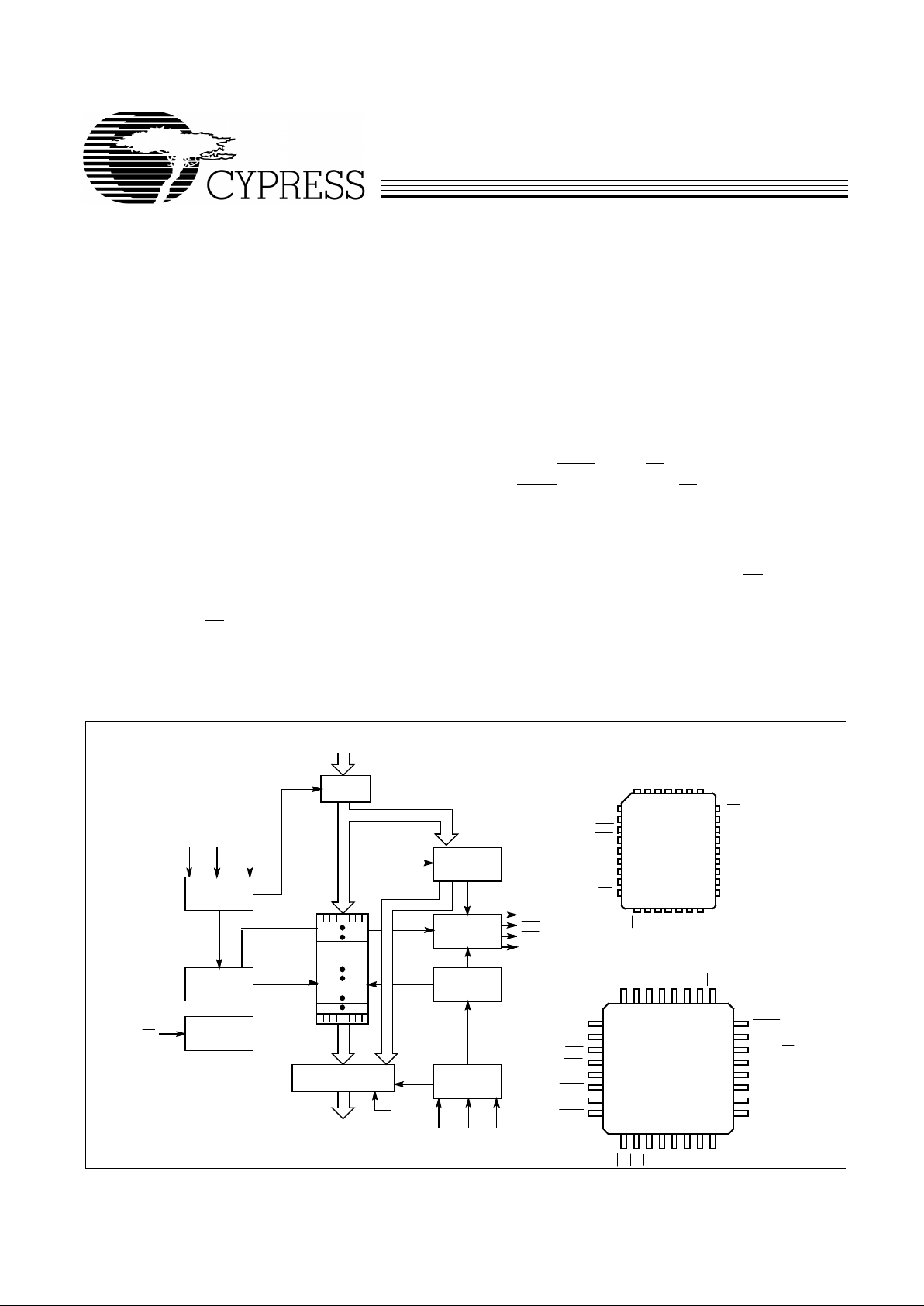
Logic Block Diagram
Pin Configuration
42X1V–1
42X1V–2
THREE-STATE
OUTPUT
REGISTER
READ
CONTROL
FLAG
LOGIC
WRITE
CONTROL
WRITE
POINTER
READ
POINTER
RESET
LOGIC
INPUT
REGISTER
FLAG
PROGRAM
REGISTER
D
0−8
RCLK
EF
PAE
PAF
Q
0−8
WEN1
WCLK
RS
OE
Dual Port
RAM Array
64x 9
8Kx 9
WEN2/LD
REN1 REN2
FF
PLCC
42X1V–3
D
1
D
0
RCLK
V
CC
D8D7D6D5D4D
3
GND
WCLK
WEN2/LD
Q
8
Q
7
D
2
D8D7D6D5D4D3D
2
PAF
PAE
5
6
7
8
9
10
11
12
13
1
2
3
4
5
6
7
8
REN1
OE
REN2
4321 313032
D
1
D
0
RCLK
GND
PAF
PAE
REN1
REN2
21
22
23
24
27
28
29
25
26
14151617181920
17
18
19
20
21
22
23
24
1415 16910111213
31 3032 2928 27 2526
Q
6
Q
5
WEN1
RS
FF
Q0Q1Q2Q3Q
4
EF
FF
Q0Q1Q2Q3Q
4
EF
OE
V
CC
WCLK
WEN2/LD
Q
8
Q
7
Q
6
Q
5
WEN1
RS
TQFP
Top View
Top View
CY7C4421V/4201V/4211V/4221V
CY7C4231V/4241V/4251V
2
Functional Description
(continued)
The CY7C42X1V provides four status pins: Empty, Full, Almost
Empty , Almost Full. The Almost Empty/Almost Full flags are programmable to single word granularity. The programmable flags default to
Empty−7 and Full−7.
The flags are synchronous, i.e., they change state relative to
either the Read Clock (RCLK) or the Write Clock (WCLK).
When entering or exiting the Empty and Almost Empty states ,
the flags are updated exclusively by the RCLK. The flags denoting Almost Full and Full states are updated exclusively by
WCLK. The synchronous flag ar chitecture guar antees that the
flags maintain their status for at least one cycle
All configurations are fabricated using an advanced 0.65µ
P-Well CMOS technology. Input ESD protection is greater than
2001V , and latch-up is pre vented b y the use of guard rings.
Selectio n Guid e
CY7C42X1V-15 CY7C42X1V-25 CY7C42X1V-35
Maximum Frequency (MHz) 66.7 40 28.6
Maximum Access Time (ns) 11 15 20
Minimum Cycle Time (ns) 15 25 35
Minimum Data or Enable Set-Up (ns) 4 6 7
Minimum Data or Enable Hold (ns) 1 1 2
Maximum Flag Delay (ns) 10 15 20
Active Power Supply
Current (mA)
Commercial 20 20 20
CY7C4421V CY7C4201V CY7C4211V CY7C4221V C Y7C4231V CY7C4241V CY7C4251V
Density 64 x 9 256 x 9 512 x 9 1K x 9 2K x 9 4K x 9 8K x 9
Pin Definitions
Signal Name Description I/O Description
D
0−8
Data Inputs I Data Inputs for 9-bit bus.
Q
0−8
Data Outputs O Data Outputs for 9-bit bus.
WEN1 W rite E n able 1 I The only write enable when device is configured to have programma ble flags. Data is
written on a LOW-to-HIGH transition of WCLK when WEN1
is asserted and FF is HIGH.
If the FIFO is configured to have two write enables, data is written on a LOW-to-HIGH transition
of WCLK when WEN1
is LOW and WEN2/LD and FF are HIGH.
WEN2/LD
Dual Mode Pin
Wr ite Enabl e 2 I If HIGH at reset, this pin operates as a second write enable. If LOW at reset, this pin
operates as a contro l to write or read the programmabl e flag offsets. WEN1
must be
LOW and WEN2 must be HIGH to write data into the FIFO. Data will not be written into the FIFO
if the FF
is LOW . If the FIFO is configured to have programmable flags, WEN2/LD is held LOW
to write or read the programmable flag offsets.
Load I
REN1, REN2 Read Enable
Inputs
I Enables the devi ce for Read operation.
WCLK Write Clock I The rising edge clocks data into the FIFO when W EN1 is LO W and WEN2/LD is HIGH
and the FIFO is not Full. When LD
is asserted, WCLK writes data into the programmable flag-off-
set register.
RCLK Read Clock I The rising edge clocks data out of the FIFO when R EN 1 and REN2 are LOW and the FIFO
is not Empty. When WEN2/LD
is LOW , RCLK reads data out of the programmable flag offset
register.
EF Empty Flag O When EF is LOW, the FIFO is empty . EF is synchronized to RCLK.
FF Full Flag O When FF is LOW, the FIFO is full . FF i s synchronized to WCLK.
PAE Programmable
Almost Empty
O When PAE is LOW, the FIFO is almost empty based on the almost empty offset value pro-
grammed into the FIFO.
PAF Programmable
Almost Full
O When PAF is LOW, the FIFO is almost full based on the almost full offset value programmed
into the FIFO .
CY7C4421V/4201V/4211V/4221V
CY7C4231V/4241V/4251V
3
Maximum Ratings
(Above which the useful lif e m ay be impaired. F or user guidelines, not tested.)
Storage Temperature ....................................... −65
°
C to +150°C
Ambient Temperature with
Po wer Applied....................................................−55
°
C to +125°C
Supply Voltage to Ground Potential..................−0.5V to +5.0V
DC V oltage Applied to Outputs
in High Z State.....................................................−0.5V to +5.0V
DC Input Voltage .................................................−0.5V to +5 . 0V
Output Current into Outputs (LOW)............................. 20 mA
Static Discharge Voltage ............. .............. ............. ...>2001V
(per MIL-STD-883, Method 3015)
Latch-Up Current.....................................................>200 mA
RS Reset I Resets device t o emp ty condition. A reset is requi red before an initia l read or write
operation after power-up.
OE Output Enable I When OE is LOW, the FIFO’s data outputs drive the bus to which they are connected. If O E is
HIGH , t he FI FO ’s outputs are in High Z (high-impedance) state.
Pin Definitions
(continued)
Signal Name Description I/O Description
Operating Range
Range Ambient Temperature V
CC
Commercial 0°C to +70°C 3.3V ± 300mV
Electrical Characteristics
Over the Operating Range
7C42X1V-15 7C42X1V-25 7C42X1V-35
Parameter Description Te st Condi tions Min. Max. Min. Max. Min. Max. Unit
V
OH
Output HIGH Voltage VCC = Min.,
I
OH
= −2.0 mA
2.4 2.4 2.4 V
V
OL
Output LOW Voltage VCC = Min.,
I
OL
= 8.0 mA
0.4 0.4 0.4 V
V
IH
Input HIGH Voltage 2.0 5.0 2.0 5.0 2.0 5.0 V
V
IL
Input LOW Voltage
−0.5
0.8
−0.5
0.8
−0.5
0.8 V
I
IX
Input Leakage
Current
V
CC
= Max.
−10
+10
−10
+10
−10
+10
µA
I
OZL
I
OZH
Output OFF,
High Z Current
OE > VIH,
V
SS
< VO < V
CC
−10
+10
−10
+10
−10
+10
µA
I
CC
[1]
Active Power Supply
Current
Com’l 20 20 20 mA
I
SB
[2]
Av erage Standby
Current
Com’l 6 6 6 mA
Capacitance
[3]
Parameter Description Test Conditions Max. Unit
C
IN
Input Capacitance TA = 25°C, f = 1 MHz,
V
CC
= 5.0V
5 pF
C
OUT
Output Capacitance 7 pF
Notes:
1. Outputs open. Tested at Frequency = 20 MHz.
2. All inputs = V
CC
– 0.2V , e x cept WCLK and RCLK, whic h are s wi tching at 20 MH z.
3. Tested initially and after any design or process changes that may affect these parameters.
CY7C4421V/4201V/4211V/4221V
CY7C4231V/4241V/4251V
4
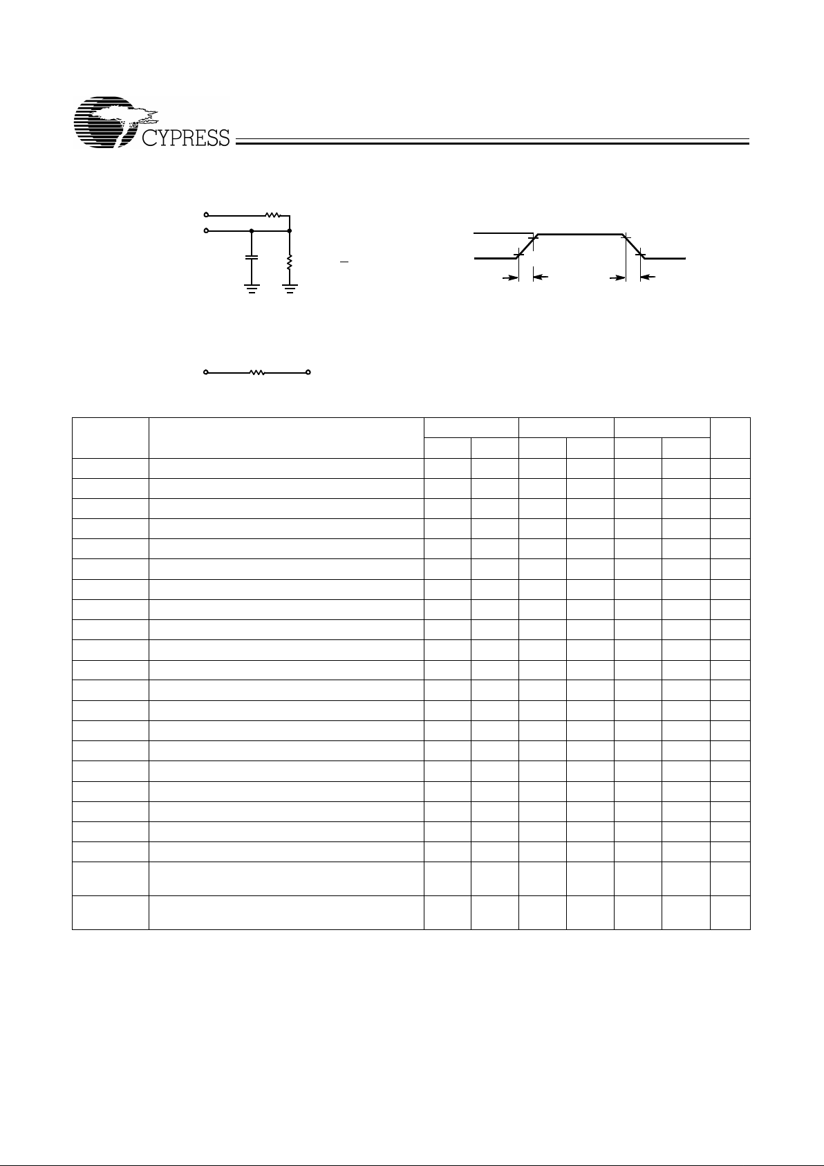
AC Test Loads and Waveforms
[4, 5]
3.0V
3.3V
OUTPUT
R1= 330
Ω
R2=510
Ω
C
L
INCLUDING
JIGA ND
SCOPE
GND
90%
10%
90%
10%
≤
3ns
≤
3
ns
OUTPUT Vth=2.0V
Equivalent to: THÉ VENIN EQUIVALENT
42X1V–4
Rth=200
Ω
ALL INPUT PULSES
42X1V–5
Switching Characteristics
Over the Operating Range
7C42X1V-15 7C42X1V-25 7C42X1V-35
Parameter D escription Min. Max. Min. Max. Min. Max. Unit
t
S
Clock Cycle Frequency 66.7 40 28.6 MHz
t
A
Data Access Time 2 11 2 15 2 20 ns
t
CLK
Clock Cycle Time 15 25 35 ns
t
CLKH
Clock HIGH Time 6 10 14 ns
t
CLKL
Clock LOW Time 6 10 14 ns
t
DS
Data Set-Up Time 4 6 7 ns
t
DH
Data Hold Time 1 2 2 ns
t
ENS
Enable Set-Up Time 4 6 7 ns
t
ENH
Enable Hold Time 1 2 2 ns
t
RS
Reset Pulse Width
[6]
15 25 35 ns
t
RSS
Reset Set-Up Time 10 15 20 ns
t
RSR
Reset Recov ery Time 10 15 20 ns
t
RSF
Reset to Flag and Output Time 18 25 35 ns
t
OLZ
Output Enable to Output in Low Z
[7]
0 0 0 ns
t
OE
Output Enable to Output Valid 3 8 3 12 3 15 ns
t
OHZ
Output Enable to Output in High Z
[7]
3 8 3 12 3 15 ns
t
WFF
Write Clock to Full Flag 11 15 20 ns
t
REF
Read Clock to Empty Flag 11 15 20 ns
t
PAF
Clock to Progra mmable A lmost- Full Fla g 18 15 20 ns
t
PAE
Clock to Progra mmable A lmost- Full Fla g 18 15 20 ns
t
SKEW1
Skew Time between Read Clock and Write Clock
for Empty Flag and Full Flag
6 10 12 ns
t
SKEW2
Skew Time between Read Clock and Write Clock
for Almost-Empty Flag and Almost-Full Flag
15 18 20 ns
Notes:
4. C
L
= 30 pF for all A C par a meters e xcept f or t
OHZ
.
5. CL = 5 pF for t
OHZ
.
6. Pulse widths less than minimum values are not allowed.
7. Values guaranteed by design, not currently tested.

CY7C4421V/4201V/4211V/4221V
CY7C4231V/4241V/4251V
5
Switching Waveforms
Notes:
8. t
SKEW1
is the min imum t ime bet ween a rising RC LK edge and a r ising WCLK ed ge t o gua rantee that FF w ill go HIGH during the current clock cycle. If the time between the
rising edge of RCLK and the risin g edge of WCLK is less than t
SKEW1
, then FF may no t c hange state unt il the ne x t WCLK rising edge .
9. t
SKEW1
is the minimum time between a rising WCLK edge and a rising RCLK edge to guarantee that EF will go HIGH during the current clock cycle. It the time between the
rising edge of WCLK and the r ising e dge of RCLK is less than t
SKEW1
, then EF ma y not chang e s tate until the ne xt RC LK risin g edge .
Write Cycle Timing
t
CLKH
t
CLKL
NO OPERATION
t
DS
t
SKEW1
t
ENS
WEN1
t
CLK
t
DH
t
WFF
t
WFF
t
ENH
WCLK
D
0–D8
FF
REN1
,REN2
RCLK
42X1V–6
NO OPERATION
WEN2
(if applic ab le)
[8]
REN1,REN2
Read CycleTiming
t
CLKH
t
CLKL
NO OPERATION
t
SKEW1
WEN1
t
CKL
t
OHZ
t
REF
t
REF
RCLK
Q
0–Q8
EF
WCLK
OE
t
OE
t
ENS
t
OLZ
t
A
t
ENH
VALID DATA
42X1V–7
WEN2
[9]

CY7C4421V/4201V/4211V/4221V
CY7C4231V/4241V/4251V
6
Notes:
10. The clocks (RCLK, WCLK) can be free-running during reset.
11. After reset, the outputs will be LOW if OE
= 0 and three- state if O E=1.
12. Holding WEN2/LD HIGH during reset w ill m ake t he pi n act as a s econd en able pin . Holding WEN2/LD LOW d uring reset will make the pin act as a load enable for the
programmab le flag of fs et regis ters .
Switching Waveforms
(continued )
t
RS
t
RSR
Q
0
−
Q
8
RS
t
RSF
t
RSF
t
RSF
OE=1
OE=0
REN1
,
REN2
EF,PAE
FF,PAF,
42X1V–8
t
RSS
t
RSR
t
RSS
t
RSR
t
RSS
WEN2/LD
WEN1
Reset Timing
[10]
[12]
[11]

CY7C4421V/4201V/4211V/4221V
CY7C4231V/4241V/4251V
7
Notes:
13. When t
SKEW1
> minimum specifica tion, t
FRL
(maximum) = t
CLK
+ t
SKEW1
. When t
SKEW1
< minimum specif ication, t
FRL
(maximum) = either 2*t
CLK
+ t
SKEW1
or t
CLK
+ t
SKEW1
.
The Latency Timing appl ies only at t he Empty B oundary (EF = LO W).
14. The first word is available the cycle after EF goe s HIG H, alw a ys.
Switching Waveforms
(continued )
D
0
(FIRSTVALIDWRITE)
First Data Word Latency after Reset with SimultaneousReadand Write
t
SKEW1
WEN1
WCLK
Q
0–Q8
EF
REN1,
REN2
OE
t
OE
t
ENS
t
OLZ
t
DS
RCLK
t
REF
t
A
t
FRL
D
1
D
2
D
3
D
4
D
0
D
1
D0–D
8
42X1V–9
t
A
WEN2
(if applicable)
[13]
[14]

CY7C4421V/4201V/4211V/4221V
CY7C4231V/4241V/4251V
8
Switching Waveforms
(continued )
DATAWRITE2
DATAWRITE1
t
ENS
t
SKEW1
DATA IN OUTPUT REGISTER
Empty F lag Timing
WEN1
WCLK
Q
0–Q8
EF
REN1,
REN2
OE
t
DS
t
ENH
RCLK
t
REF
t
A
t
FRL
D0–D
8
DATA READ
t
SKEW1
t
FRL
t
REF
t
DS
t
ENS
t
ENH
42X1V–10
t
ENS
WEN2
(if applicable)
t
ENH
t
ENS
t
ENH
t
REF
LOW
[13] [13]

CY7C4421V/4201V/4211V/4221V
CY7C4231V/4241V/4251V
9
Notes:
15. t
SKEW2
is the minimum time between a ris ing WCLK and a rising RCLK edge f or P AE to chang e state during that clock cycle. If the time bet ween the edge of WCLK and the
rising RCLK is les s than t
SKEW2
, then PAE may not change state unt il the ne x t R CLK.
16. PAE offset = n.
17. If a read is performed on this rising edge of the read clock, there will be Empty + (n−1) words in the FIFO when PAE
goes LOW.
Switching Waveforms
(continued )
Full Flag Timing
Q0–Q
8
REN1,
REN2
WEN1
WEN2
(if applic ab le)
D
0–D8
NEXT DATA READ
DATA WRITE
NO WRITE
DATA IN OUTPUT REGISTER
FF
WCLK
OE
RCLK
t
A
DATA READ
t
SKEW1
t
DS
t
ENS
t
ENH
t
WFF
t
A
t
SKEW1
t
ENS
t
ENH
t
WFF
DATA WRITE
NO WRITE
t
WFF
LOW
42X1V–11
NO WRITE
[8]
[8]
t
ENH
Programmable Almost Empty Flag Timing
WCLK
PAE
RCLK
t
CLKH
t
ENS
t
CLKL
t
ENS
t
PAE
N + 1 WORDS
INFIFO
42X1V–12
t
ENH
t
ENS
t
ENH
t
ENS
t
PAE
REN1,
REN2
WEN1
WEN2
(if applic ab le)
t
SKEW2
[15]
Note 16
Note 17

CY7C4421V/4201V/4211V/4221V
CY7C4231V/4241V/4251V
10
Notes:
18. If a write is performed on this rising edge of the write clock, there will be Full – (m–1) words of the FIFO when PAF
goes LOW.
19. PAF offset = m.
20. 64–m words for CY7C4421V, 256-m words in FIFO for CY7C4201V, 512–m words for CY7C4211V, 1024–m words for CY7C4221V, 2048–m words for
CY7C4231V, 4096–m words for CY7C4241V, 8192–m words for CY7C4251V.
21. t
SKEW2
is the minimum t ime betw een a rising RCL K edge a nd a r ising WC LK edge for P AF to change during t hat cl ock cycle. If the time between the rising edge of RCLK
and the rising edge o f WCLK i s les s than t
SKEW2
, then PAF may not change state until th e ne x t WCLK.
Switching Waveforms
(continued )
t
ENH
ProgrammableAlmost Ful l Fl ag Timing
WCLK
PAF
RCLK
t
CLKH
t
ENS
FULL −M WORDS
IN FIFO
t
CLKL
t
ENS
FULL −M+1 WORDS
IN FIFO
42X1V–13
t
ENH
t
ENS
t
ENH
t
ENS
t
PAF
REN1,
REN2
WEN1
WEN2
(if applic ab le)
t
SKEW2
t
PAF
Note 18
Note 19
[20]
[21]
t
ENH
Write Programmable Registers
WEN2/LD
WCLK
t
CLKH
t
ENS
t
CLKL
PAE OFFSET
LSB
D
0–D8
WEN1
t
ENS
PAF OFFSET
MSB
t
CLK
t
DS
t
DH
42X1V–14
PAE OFFSET
MSB
PAF OFFSET
LSB

CY7C4421V/4201V/4211V/4221V
CY7C4231V/4241V/4251V
11
Architecture
The CY 7C42X1 V con sist s of an arr a y of 64 to 8K wo rds o f 9 bi ts
each (implemented by a du al-port array of SRAM cells), a read
pointer, a wr ite poin ter, control s ignals ( RCLK, W CLK, R EN1
,
REN2
, WEN1, WEN2, RS), and flags (EF, PAE , PAF, FF).
Resetting the FIFO
Upon power-up, the FIFO must be reset with a Reset (RS)
cycle. This causes the FIFO to enter the Empty condition signifi ed by EF
being LOW. All data outputs (Q
0−8
) go LOW t
RSF
after the ris ing edge of RS. In order for the FIFO to reset to its
default state, a falling edge must occur on RS
and the user
must not read or write while RS
is LOW. All flags are guaran-
teed to be valid t
RSF
after RS is taken LOW.
FIFO Operation
When the WEN1 signal is active LOW and WEN2 is active HIGH,
data present on th e D
0−8
pins is written into the FIFO on each
rising edge of the WCLK signal. Similarly, when the REN1
and
REN2
signals are active LOW, data in the FIFO memory will
be presented on th e Q
0−8
outputs. New data wi ll be prese nte d
on each rising edge of RCLK while REN1
and REN2 are ac-
tive. REN1
and REN2 must set up t
ENS
before RCLK for it to
be a valid read function. WEN1
and WEN2 must occur t
ENS
before WCLK for it to be a valid write function.
An Output Enable (OE
) pin is provided to three-state the Q
0−8
outputs when OE is asserted. When OE is enabled (LOW), data
in the output register will be available to the Q
0−8
outputs after tOE.
The FIFO contains overflow circuitry to disallow additional
writes when the FIFO is full, and underflow circuitry to disallo w
additional reads when the FIFO is empty. An empty FIFO
maintains the data of the last valid read on its Q
0−8
outputs
ev en aft e r additional reads occur.
Write Enable 1 (WEN1
)
- If the FIFO is configured for pro-
grammab le flags, Write Enable 1 (WEN1
) is the only wri te enable control pin. In this configuration, when Write Enable 1
(WEN1
) is LOW, data can be loade d int o the i nput r egist er and
RAM array on t he LO W-to-HIGH trans iti on of e v ery write cloc k
(WCLK). Data is stored is the RAM array sequentially and independently of any on-going read operat ion.
Write Enable 2/Load ( WEN2/LD
)
- This is a dua l-purpose pin.
The FIFO is configured at Reset to have programmable flags
or to hav e two write enab les, which all ows f or depth ex pansion.
If Write Enabl e 2 /Load ( WEN2/L D
) is set active HIGH at Reset
(RS
=LOW), this pin operates as a second write enable pin.
If the FIFO is con figured t o hav e two write enables , when Write
Enable (WEN1
) is LOW and W rit e Enable 2/Load (WEN2/L D)
is HIGH, data can be loaded into the input register and RAM
array on the LOW-to-HIGH transition of every write clock
(WCLK). Data is stored in the RAM array sequentially and independently of any on-going read operation.
Programming
When WEN2/LD is h eld LO W duri ng Reset , this pin i s the load
(LD
) enable for flag offset programming. In this configuration,
WEN2/LD
can be used to access t he f our 8-bit offset regis ters
contained in the CY7C42X1V for writing or reading data to
these registers.
When the device is configured for programmable flags and
both WEN2/LD
and WEN1 are LOW, the first LOW-to-HIGH
transition of WCLK writes dat a from the data inputs to the empty offset Least Signifi cant Bit (LSB) reg ister . The second, thi rd,
and fourth LOW -to-HIGH tr ansiti ons of WCLK store dat a in the
empty offset Most Si gnifica nt Bit (MSB) reg ister , full o ffset LSB
register, and full offset MSB register, respectively, when
WEN2/LD
and WEN1 are LOW. The fifth LOW-to-HIGH tran-
sition of WCLK while WEN2/LD
and WEN1 are LOW writes
data to the em pty LSB register again. Figure 1 shows the register sizes a nd default values for the vari ous device types.
It is not nece ssary to writ e to all t he offset registe rs at one time.
A subset of the offset registers can be written; then b y bringing
the WEN 2/ LD
input HIGH, the FIFO is re turned to normal read
and write oper ati on. The ne xt time WEN2/LD
is brought LOW,
a write operation stores data in the next offset register in sequence.
The contents of the offset registers can be read to the data
outputs when WEN2/LD
is LOW and both REN1 and REN2
are LOW. LOW-to-HI GH transi tions of RCLK read regi ster con tents to the data outputs. Writes and reads should not be
performed simul taneously on the offset registers.
Switching Waveforms
(continued )
PAF OFFSET
MSB
PAF OFFSET
LSB
t
ENH
Read Pr ogrammable Registers
WEN2/LD
RCLK
t
CLKH
t
ENS
t
CLKL
PAE OFFSET LSB
Q
0–Q8
REN1,
REN2
t
ENS
PAE OFFSET MSB
t
CLK
UNKNOWN
t
A
42X1V–15

CY7C4421V/4201V/4211V/4221V
CY7C4231V/4241V/4251V
12
Programmable Fla g (PAE
, PAF) Operation
Whether the fl ag offset regi sters are prog rammed as described
in Table 1 or the default values are used, the programmable
Almost Empty Flag (PAE
) and programmab l e Almost Ful l Flag
(PAF
) states are d etermined b y thei r corresp ondi ng o ffset r eg-
isters and the difference between the read and write pointers.
The number formed by the empty offset least significant bit
register and empty offset most significant register is referred
to as n and determines the operation of PAE
. PAE is synchronized to the LOW-to-HIGH transition of RCLK by one flip-flop
and is LOW when the FIFO contai ns n or f ewer unre ad words .
PAE
is set HIG H by th e LOW -to-HI GH transit ion of RCLK when
the FIFO contains (n+1) or greater unread words.
The number formed by t he full offset least signif icant bit regis-
ter and full offset most significant bit register is referred to as
m and determines th e operation of PAF
. PAE is synchroniz ed
to the LOW -to-H IGH transit ion of WCLK by one flip- flop and is
set LOW when the number of unread words in the FIFO is
greater than or equal to CY7C4421V (64 − m), CY7C4201V
(256 − m), CY7C4211V (512 – m ), CY7C4221V (1K − m),
CY7C4231V (2K − m), CY7C4241V (4K − m), and
CY7C4251V (8K − m). PAF
is set HIGH by the LOW-to-HIGH
transition of WCLK when the number of available memory locations is grea ter than m.
Note:
22. The same selection sequence applies to reading from the registers. REN1
and REN2 are enab led and a re ad is perf ormed on the L OW - to-HIG H tra nsition of R CLK.
Figure 1. Offset Register Locati on and Default Valu es
64 x 9 256 x 9512x9
8
0
8
0
8
0
8
0
1K x 9
2Kx9 4Kx9 8Kx
9
(MSB)
0
(MSB)
0
7
7
8
0
8
0
8
0
8
0
(MSB)
00
(MSB)
00
7
1
7
1
8
0
8
0
8
0
8
0
(MSB)
000
(MSB)
000
7
2
7
2
8
0
8
0
8
0
8
0
Empty Offset(LSB) Reg.
Default Value = 007h
FullOffset(LSB)Reg
Default Value = 007h
(MSB)
0000
(MSB)
0000
7
3
7
3
Empty Offset(LSB) Reg.
Default Value = 007h
FullOffset(LSB)Reg
Default Value = 007h
Empty Offset (LSB) Reg.
Default Value = 007h
FullOffset(LSB)Reg
Default Value = 007h
Empty Offset (LSB) Reg.
DefaultValue= 007h
FullOffset(LSB)Reg
DefaultValue=
007h
8
0
8
0
8
0
8
0
Empty Offset (LSB) Reg.
DefaultValue= 007h
FullOffset(LSB)Reg
DefaultValue= 007h
(MSB)
00000
(MSB)
00000
7
4
7
4
8
0
8
0
8
0
8
0
6
6
FullOffset(LSB) Reg
DefaultValue= 007h
Empty Offset(LSB) Reg.
DefaultValue=
007h
8
0
8
0
8
0
8
0
7
7
FullOffset(LSB)Reg
DefaultValue= 007h
Empty Offset (LSB) Reg.
DefaultValue=
007h
Table 1. Writing the Offset Registers
LD WEN WCLK
[22]
Selection
0 0 Empty Offset (LSB)
Empty Offset (MSB)
Full Offset (LSB)
Full Offset (MSB)
0 1 No O p eratio n
1 0 Write Into FIFO
1 1 No O p eratio n

CY7C4421V/4201V/4211V/4221V
CY7C4231V/4241V/4251V
13
Width Expansion Configuration
Word width may be i ncreased simply by connecting the corresponding input control signals of mult iple devices . A composite
flag should be created for each of the end-point status flags
(EF
and FF). The partial status flags (PAE and PAF) can be
detected f rom any one device. Figure 2 demonstrat es a 18-bit
word width by usin g two CY7C42X1Vs. An y word width can be
attained b y adding additional CY7C42X1Vs.
When the CY7C42X1 V is i n a Widt h Exp ansion Co nfigur ati on,
the Read Enable (REN2
) control input can be grounded (see
Figure 2). In this configuration, the Write Enable 2/Load
(WEN2/LD
) pin is set to LOW at Reset so that the pin ope rates
as a control to load and read t he programmable flag offset s.
Flag Ope r ati o n
The CY7C42X1 devices provide four flag pins to indicate the
condition of the FIFO con tents . Empty, Full, P AE
, and PAF are
synchronous.
Full Flag
The Full Flag (FF
) will go LOW when de vi ce is f ull. Write oper-
ations are inhibited whenever FF
is LOW regardless of the
state of WEN1
and WEN2/LD. FF is synchronized to WCLK,
i.e., it is exclusivel y updated by each rising edge of WCLK.
Empty Flag
The Empty Flag (EF
) will go LOW when the device is empty.
Read operations are inhibited whenever EF
is LOW, regard-
less of the state of REN1
and REN2. EF is synchronized to
RCLK, i.e., it is exclusively updated by each rising edge of
RCLK.
Table 2. Status Flags
Number of Wor ds in FIFO
FF PAF PAE EFCY7C4421V CY7C4201V CY7C4211V
0 0 0 H H L L
1 to n
[23]
1 to n
[23]
1 to n
[23]
H H L H
(n+1) to 32 (n+1) to 128 (n+1) to 256 H H H H
33 to (64−(m+1)) 129 to (256−(m+1)) 257 to (512−(m+1)) H H H H
(64−m)
[24]
to 63 (256−m)
[24]
to 255 (512−m)
[24]
to 511 H L H H
64 256 512 L L H H
Number of Wo rds in FIFO
FF PAF PAE EFCY7C4221V CY7C4231V CY7C4241V CY7C4251V
0 0 0 0 H H L L
1 to n
[23]
1 to n
[23]
1 to n
[23]
1 to n
[23]
H H L H
(n+1) to 512 (n+1) to 1024 (n+1) to 2048 (n+1) to 4096 H H H H
513 to (1024 −(m+1)) 1025 to (2048 −(m+1)) 2049 to (4096 −(m+1)) 4097 to ( 8192 −(m+1)) H H H H
(1024−m)
[24]
to 1023 (2048−m)
[24]
to 2047 (4096−m)
[24]
to 4095 (8192−m)
[24]
to 8191 H L H H
1024 2048 4096 8192 L L H H
Notes:
23. n = Empty Offset (n=7 default value).
24. m = Full Offset (m=7 default value).

CY7C4421V/4201V/4211V/4221V
CY7C4231V/4241V/4251V
14
Figure 2. Block Di agram of 64 x 9, 256 x 9, 512 x 9, 1024 x 9, 2048 x 9, 4096 x 9, 8192 x 9 Low Voltage Synchronous FIFO
Memory Used in a Width Expansion Configuration
42X1V–16
FF
FF
EF
EF
WRITE CLOCK(WCLK)
RITE ENABLE1(WEN1
)
WRITE ENABLE2/LOAD
(WEN2/LD)
PROGRAMMABLE (PAF
)
FULLFLAG(FF
)# 1
CY7C42X1V
918
DATA IN (D)
RESET
(RS)
9
RESET(RS)
READ CLOCK(RCLK)
READ ENABLE1 (REN1
)
OUTPUT ENABLE (OE
)
PROGRAMMABLE (PAE
)
EMPTY FLAG (EF
)#1
9
DATA OUT (Q)
9 18
ReadEnable2 (REN2)
CY7C42X1V
EMPTY FLAG(EF) #2
FULLFLAG(FF
)# 2
Read Enable2
(REN2)
Ordering Information
64 x 9 Low V oltage Synchronous FIFO
Speed (ns) Ordering Code Package Nam e Pack age Type Operating Range
15 CY7C4421V-15AC A32 32-Lead Thin Quad Flatpack Comme rcial
CY7C4421V-15JC J65 32-Lead Plastic Leaded Chip Carrier
25 CY7C4421V-25AC A32 32-Lead Thin Quad Flatpack Comme rcial
CY7C4421V-25JC J65 32-Lead Plastic Leaded Chip Carrier
35 CY7C4421V-35AC A32 32-Lead Thin Quad Flatpack Comme rcial
CY7C4421V-35JC J65 32-Lead Plastic Leaded Chip Carrier
256 x 9 Low Voltage Synchronous FIFO
Speed (ns) Ordering Code Package Name Package Type Operating Range
15 CY7C4201V-15AC A32 32-Lead Thin Quad Flatpack Commercial
CY7C4201V-15JC J65 32-Lead Plastic Lea ded Chip Carrier
25 CY7C4201V-25AC A32 32-Lead Thin Quad Flatpack Commercial
CY7C4201V-25JC J65 32-Lead Plastic Lea ded Chip Carrier
35 CY7C4201V-35AC A32 32-Lead Thin Quad Flatpack Commercial
CY7C4201V-35JC J65 32-Lead Plastic Lea ded Chip Carrier

CY7C4421V/4201V/4211V/4221V
CY7C4231V/4241V/4251V
15
Document #: 38-00622-Al
Ordering Information
(continued)
512 x 9 Low Voltage Synchronous FIFO
Speed (ns) Ordering Code Package Name Package Type Operating Range
15 CY7C4211V-15AC A32 32-Lead Thin Quad Flatpack Commercial
CY7C4211V-15JC J65 32-Lead Plastic Leaded Chi p Carrier
25 CY7C4211V-25AC A32 32-Lead Thin Quad Flatpack Commercial
CY7C4211V-25JC J65 32-Lead Plastic Leaded Chi p Carrier
35 CY7C4211V-35AC A32 32-Lead Thin Quad Flatpack Commercial
CY7C4211V-35JC J65 32-Lead Plastic Leaded Chi p Carrier
1K x 9 Low Vo ltage Synchronous FIFO
Speed (ns) Ordering Code Package Name Package Type Operating Range
15 CY7C4221V-15AC A32 32-Lead Thin Quad Flatpack Commercial
CY7C4221V-15JC J65 3 2-Lead Plastic Leaded Chip Carrier
25 CY7C4221V-25AC A32 32-Lead Thin Quad Flatpack Commercial
CY7C4221V-25JC J65 3 2-Lead Plastic Leaded Chip Carrier
35 CY7C4221V-35AC A32 32-Lead Thin Quad Flatpack Commercial
CY7C4221V-35JC J65 3 2-Lead Plastic Leaded Chip Carrier
2K x 9 Low Vo ltage Synchronous FIFO
Speed (ns) Ordering Code Pack age Name Package Type Operating Range
15 CY7C4231V-15AC A32 32-Lead Thin Quad Flatpack Commercial
CY7C4231V-15JC J65 32-Lead Plastic Leaded Chip Carrier
25 CY7C4231V-25AC A32 32-Lead Thin Quad Flatpack Commercial
CY7C4231V-25JC J65 32-Lead Plastic Leaded Chip Carrier
35 CY7C4231V-35AC A32 32-Lead Thin Quad Flatpack Commercial
CY7C4231V-35JC J65 32-Lead Plastic Leaded Chip Carrier
4K x 9 Low Vo ltage Synchronous FIFO
Speed (ns) Ordering Code Package Name Package Type Operating Range
15 CY7C4241V-15AC A32 32-Lead Thin Quad Flatpack Commercial
CY7C4241V-15JC J65 32-Lead Plastic Leaded Chip Carrier
25 CY7C4241V-25AC A32 32-Lead Thin Quad Flatpack Commercial
CY7C4241V-25JC J65 32-Lead Plastic Leaded Chip Carrier
35 CY7C4241V-35AC A32 32-Lead Thin Quad Flatpack Commercial
CY7C4241V-35JC J65 32-Lead Plastic Leaded Chip Carrier
8K x 9 Low Vo ltage Synchronous FIFO
Speed (ns) Ordering Code Package Name Pack age Type Operating Range
15 CY7C4251V-15AC A32 32-Lead Thin Quad Flatpack Commercial
CY7C4251V-15JC J65 32-Lead Plastic Leaded Chip Carrier
25 CY7C4251V-25AC A32 32-Lead Thin Quad Flatpack Commercial
CY7C4251V-25JC J65 32-Lead Plastic Leaded Chip Carrier
35 CY7C4251V-35AC A32 32-Lead Thin Quad Flatpack Commercial
CY7C4251V-35JC J65 32-Lead Plastic Leaded Chip Carrier

CY7C4421V/4201V/4211V/4221V
CY7C4231V/4241V/4251V
© Cypress Semiconductor Corporation, 1999. The information contained herein is subject to change without notice. Cypress Semiconductor Corporation assumes no responsibility for the use
of any circuitry other than circuitry embodied in a Cypress Semiconductor product. Nor does it con vey or imply any license under patent or other rights. Cypress Semiconductor does not authorize
its products for use as critical components in life-support systems where a malfunction or failure may reasonably be expected to result in significant injury to the user. The inclusion of Cypress
Semiconductor products in life-support systems application implies that the manufacturer assumes all risk of such use and in doing so indemnifies Cypress Semiconductor against all charges.
Package Diagrams
32-Lead Thin Plastic Quad Flatpack 7 x 7 x 1.0mm A32
51-85063-B
32-Lead Plastic Leaded Chip Carrier J65
51-85002-B
 Loading...